EP0896202A2 - Verfahren und Vorrichtung zur Inspektion eines Elementes einer Anordnung - Google Patents
Verfahren und Vorrichtung zur Inspektion eines Elementes einer Anordnung Download PDFInfo
- Publication number
- EP0896202A2 EP0896202A2 EP98114769A EP98114769A EP0896202A2 EP 0896202 A2 EP0896202 A2 EP 0896202A2 EP 98114769 A EP98114769 A EP 98114769A EP 98114769 A EP98114769 A EP 98114769A EP 0896202 A2 EP0896202 A2 EP 0896202A2
- Authority
- EP
- European Patent Office
- Prior art keywords
- lens
- array
- image forming
- image
- lens array
- Prior art date
- Legal status (The legal status is an assumption and is not a legal conclusion. Google has not performed a legal analysis and makes no representation as to the accuracy of the status listed.)
- Withdrawn
Links
Images


Classifications
-
- G—PHYSICS
- G01—MEASURING; TESTING
- G01B—MEASURING LENGTH, THICKNESS OR SIMILAR LINEAR DIMENSIONS; MEASURING ANGLES; MEASURING AREAS; MEASURING IRREGULARITIES OF SURFACES OR CONTOURS
- G01B11/00—Measuring arrangements characterised by the use of optical techniques
- G01B11/14—Measuring arrangements characterised by the use of optical techniques for measuring distance or clearance between spaced objects or spaced apertures
-
- G—PHYSICS
- G01—MEASURING; TESTING
- G01B—MEASURING LENGTH, THICKNESS OR SIMILAR LINEAR DIMENSIONS; MEASURING ANGLES; MEASURING AREAS; MEASURING IRREGULARITIES OF SURFACES OR CONTOURS
- G01B11/00—Measuring arrangements characterised by the use of optical techniques
- G01B11/02—Measuring arrangements characterised by the use of optical techniques for measuring length, width or thickness
- G01B11/024—Measuring arrangements characterised by the use of optical techniques for measuring length, width or thickness by means of diode-array scanning
Definitions
- the present invention relates to a method of examining an array element in which plural elements are arrayed in a predetermined arrangement and an array element examination device, particularly to a method and a device which are suitable for examination of fiber positions in a fiber array block.
- the entire array element is photographed by, for example, a CCD camera or the like, photographing signals are image-processed, and a position of each element is obtained.
- a relative position of each element is obtained from the movement of the stage.
- the conventional examination method is constituted as aforementioned, but recently the elements have been increasingly made fine. Therefore, an element position precision of 1 ⁇ m or less is also increasingly requested for.
- a photographing range is limited in order to obtain a high resolution.
- the range is limited to several tens of ⁇ m.
- an object of the invention is to provide an array element examination method and an array element examination device which can examine a position of an array element with a high resolution, in a broad range and relatively inexpensively.
- positions of plural elements arranged in an array state are detected by using an optical detector.
- Lights from the plural elements are fetched by a lens array which has plural lenses with optical axes corresponding to the elements arranged substantially parallel with one another, an image of a light from each lens of the lens array is formed within a light receiving region of the detecting means by an image forming lens, the formed image of the element is detected, and a position of each element is obtained from a detection signal.
- the lights of plural elements are formed into images within the light receiving region of the detecting means. Therefore, as compared with the method in which plural elements are entirely photographed as they are, examination can be made with a higher resolution and in a broader range, and measurement can be performed relatively inexpensively. Additionally, if there is no error in a measurement system, for example, if there is no pitch error or the like in plural elements, then the images of plural elements are formed in a predetermined position (the identical point or the like) in the light receiving region of the detecting means. If there is a pitch error or the like, however, the images are formed in positions deviated from the predetermined position, and it can be easily determined from the deviation whether or not the array element is good. Specifically, the array element is an optical fiber.
- a lens array in which plural lenses corresponding to the plural elements and having focal lengths f 1 equal to the substantially mutually parallel optical axes are arranged in such a manner that the coordinate of the optical axis of the i-th lens in a plane perpendicular to the optical axis of each lens is represented by (X1 i , Y1 i ) and an image forming lens having a focal length f 2 for forming an image of a light from each lens of the lens array.
- the lens array and the image forming lens form an image of each element within a plane of a detecting surface in the light receiving region of the detecting means which is perpendicular to the optical axes of the lenses constituting the lens array
- the lens array and the image forming lens are arranged relative to plural elements in such a manner that relationships of the following expressions (1) to (3) are satisfied.
- the light from the i-th element among the plural elements is fetched by the i-th lens in the lens array, and the fetched light is formed into an image in a desired position (Xs i , Ys i ) on the detecting surface by the image forming lens.
- the formed image of each element is detected, and the position of each element is obtained from a detection signal.
- the image of each element can be formed in an arbitrary position on an examining surface, plural elements can be observed once. Moreover, by determining each parameter in the above expression (3), even if the lens of the same focal distance is used, the magnification of the optical system can be changed. Additionally, by changing the sign of the magnification, an erected or inverted element image can be freely selected.
- the measurement system when the light from each element is formed into the image on substantially the identical point within the detecting surface the measurement system can be constituted without any movable section, and a highly precise position detection can be performed.
- the magnification M does not depend on k or is not influenced by an error of k. It becomes difficult to be influenced by errors, and an accurate measurement can be made.
- a first array element examination device of the invention is a device for performing the first array element examination method.
- the array element examination device for detecting positions of plural elements arranged in an array state is provided with a lens array having plural lenses corresponding to the plural elements and having optical axes arranged substantially parallel with one another, at least one image forming lens for forming an image of a light from each lens of the lens array within a light receiving region of a detecting means, a detecting means for detecting the formed image of the element and an arithmetic operation circuit for obtaining the position of each element from a detection signal of the detecting means.
- the lens array, the image forming lens and the detecting means are arranged in such a manner that the light from each lens of the lens array is formed into the image within the light receiving region of the detecting means.
- the element image is preferably photographed with, for example, a CCD camera or detected with a split-type photo diode. Since lights of plural elements are formed into images within the light receiving region of the detecting means, a measurement system constituted of the lens array, the image forming lens, the detecting means and the arithmetic operation circuit does not require any movable section. Therefore, positions can be detected highly precisely.
- a second array element examination device of the invention is a device for performing the second array element examination method.
- a lens array in which plural lenses corresponding to the plural elements and having focal lengths f 1 equal to the substantially mutually parallel optical axes are arranged in such a manner that the coordinate of the optical axis of the i-th lens in a plane perpendicular to the optical axis of each lens is represented by (X1 i , Y1 i ) and an image forming lens having a focal length f 2 for forming images of lights from the lens array in a plane of a detecting surface within a light
- the light from the i-th element among the plural elements is formed into the image in a desired position (Xs i , Ys i ) of the detecting surface by the i-th lens in the lens array and the image forming lens.
- the device is provided with the detecting means for detecting the formed image of each element and an arithmetic operation circuit for obtaining the position of each element from a detection signal of the detecting means.
- a screen is disposed on a plane of the array-element image formed by the image forming lens, and the image projected on the screen is preferably photographed.
- the array element examination device is preferably constituted in such a manner that the element as the examination object and the corresponding array lens are arranged close to each other.
- the close arrangement of the detection object or element and the corresponding array lens facilitates the positioning when setting the element.
- an opening is preferably disposed for selectively passing the light from only one element among the plural elements.
- a wavelength filter is disposed before and/or behind the lens array, and further a filter whose transmission wavelength is variable is preferably disposed before the detecting means.
- the wavelength filter By disposing the wavelength filter before and/or behind the lens array corresponding to each element, the element can be identified by color.
- the filter whose transmission wavelength is variable before the detecting means the detecting means may be a monochromatic detector.
- variable wavelength light source is preferably used as a lighting means for transmitting or reflecting lights to the array element. Even when the variable wavelength light source is used as the lighting means for transmitting or reflecting lights to plural elements as the examination objects instead of the variable wavelength filter, the same effect can be obtained.
- diffractive lenses are preferably used in the lens array.
- a degree of freedom in design is increased as compared with the refractive lenses.
- an off-axis optical system is preferably used partially in the lens array.
- the off-axis optical system is preferably used in a part of the lens array.
- a lens with a larger F number can be obtained.
- a measurement with a brightness and a high resolution can be realized.
- the array element examination device it is preferable that the array element is a fiber array and a monochromatic or white light is radiated from an end face opposite to the fiber as the lighting means.
- the examination object is the optical fiber array, and the monochromatic or white light is radiated from the end face opposite to the fiber as the lighting means and a light emitted from the examination end face is detected, a core position can be obtained more accurately.
- a split-type photo diode is preferably used as an image detecting means.
- the split-type photo diode is used as the image detecting means, biasing of each image can be seen by taking a difference in the quantity of light detected by each photo diode. Therefore, detection can be performed remarkably inexpensively and at a higher rate as compared with the image processing which requires a complicated arithmetic operation.
- Fig. 1 is a schematic diagram showing an embodiment of an array element examination device according to the invention.
- Fig. 2 is a schematic diagram showing an embodiment in which a screen is disposed behind an image forming lens.
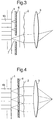
- Fig. 3 is a schematic diagram showing an embodiment in which a shielding plate provided with an opening is movably disposed before a lens array.
- Fig. 4 is a schematic diagram showing an embodiment of the array element examination device in which a wavelength filter is disposed before the lens array.
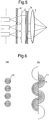
- Fig. 5 is a schematic diagram showing an embodiment of the array element examination device in which the wavelength filter is disposed before the lens array and a variable wavelength filter is disposed behind the lens array.
- Fig. 6 is a front view showing an embodiment of an objective lens as seen from an optical axis direction: Fig. 6A shows a normally arranged optical system and Fig. 6B shows an off-axis optical system.
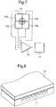
- Fig. 7 is a schematic diagram showing an embodiment in which a split-type photo diode is used as detecting means.
- Fig. 8 is a perspective view showing a main portion of an embodiment of a fiber array block as an examination object.
- Fig. 9 shows each parameter of the optical system in an embodiment of the array element examination device according to the invention.
- Fig. 10 shows an embodiment in which by adjusting the arrangement of each lens of the lens array, an end-face image of each fiber is formed in a different position of a detecting surface:
- Fig. 10A shows the arrangement of each lens of the lens array and
- Fig. 10B shows an end-face image of each fiber dispersed and formed on a photographing surface.
- Fig. 1 is a schematic diagram of an array element examination device of the invention, which is constituted of a lens array 2, an image forming lens 3, a CCD camera 4 and a computer 5 as an arithmetic operation circuit provided with a display device.
- An examination object is a fiber array 1 in which array elements with a diameter of 125 ⁇ m are arranged at a pitch of 250 ⁇ m in a row.
- Fig. 8 shows an appearance of a fiber array block 15 constituting the fiber array 1.
- the lens array 2 of integrally arranged refractive lenses as objective lenses for making parallel lights from the fiber array 1 is used. Therefore, pitch precision levels of lenses 2b constituting the lens array 2 are secured at the same degrees as those of fibers 1b of the fiber array 1.
- the lens array 2 is prepared by etching a quartz substrate using a lithography technique, and has a pitch of 250 ⁇ m, a diameter of 246 ⁇ m and a focal length of 2 mm. By using the lithography technique, a precision with a pitch error of 0.1 ⁇ m or less can be obtained.
- a fiber end face 1a is set on a focal plane of the lens array 2.
- an achromatic lens with a focal length of 40 mm and a diameter of 30 mm is used, and the CCD camera 4 is disposed as the image detecting means on an image-side focal position.
- a fiber end-face image is formed in a light receiving region of the CCD camera 4, specifically on the substantially identical point on a photographing surface by the corresponding lens array 2 and the image forming lens 3.
- the magnification is determined by the ratio of the focal lengths of the lens array 2 and the image forming lens 3, and is 20 times in the embodiment.
- a picture element size of the CCD camera 4 is 11 ⁇ 13 ⁇ m, and a resolution per picture element is 0.55 or 0.65 ⁇ m.
- an interpolation processing is performed to obtain a resolution of one tenth of the above value.
- an image processing an image forming position is obtained in a unit of one picture element, the picture element unit is converted to a length unit based on the picture element size, and a relative position of the image forming position obtained in the length unit is obtained.
- the fiber array 1 is arranged accurately at the pitch of 250 ⁇ m, all fiber end-face images are formed on the identical point, but if there is a pitch error in the fiber array 1, deviation is made 20 times larger when forming the image.
- the processing in the computer 5 it is determined whether or not the fiber array 1 is good. Additionally, the arithmetic operation results and the images of the fibers 1b are displayed on the display device of the computer 5.
- the image formed by the image forming lens 3 is taken directly by the CCD camera 4, but a magnifying optical system, e.g., a lens may be inserted between the image forming lens and the CCD camera. In this case, the resolution can be enhanced.
- a magnifying optical system e.g., a lens may be inserted between the image forming lens and the CCD camera. In this case, the resolution can be enhanced.
- a screen 16 may be disposed on a first image plane of the image forming lens 3 to photograph an image on the screen. By photographing the image projected on the screen, a clearer cage can be detected.
- the embodiment uses a constitution in which a focal position of the lens array 2 is outside a lens substrate 2a constituting the lens array 2, but may use a constitution which is prepared in such a manner that a focus is on a substrate surface and that the end face 1a of the fiber array 1 is close to the lens substrate 2a.
- this constitution when the elements as the measurement objects are set, positioning/alignment is facilitated.
- each fiber 1b is disposed in the focal position of the corresponding lens 2b, images can be formed on the identical point with a simple optical system.
- a shielding plate 6 provided with one opening 7 may be movably disposed in a direction orthogonal to optical axes between the fiber array 1 and the lens array 2, so that the images of the fibers 1b are formed one by one by using the opening 7 of the shielding plate 6. Thereby, the position of each fiber 1b can be measured. Additionally, by providing plural openings, positions of plural fibers can be measured. Moreover, the opening may be formed between the lens array 2 and the image forming lens 3. Specifically, a pin hole may be formed as the opening.
- a wavelength filter 8 whose wavelength differs with each fiber 1b is disposed before the lens array 2, and the using of the wavelength filter 8 enables each fiber 1b to be distinguished by color.
- the wavelength filter 8 may be disposed behind the lens array 2.
- the variable wavelength filter 9 when a variable wavelength filter 9 is used between the lens array 2 and the image forming lens 3, the fiber 1b can be identified even by a monochromatic CCD camera by controlling a transmission wavelength.
- the variable wavelength filter 9 can be constituted of a liquid crystal filter.
- a variable wavelength light source (not shown) may be used as a lighting means for transmission or reflection for the elements to light the elements.
- diffractive lenses 10 as shown in Fig. 6A may be used.
- the using of the diffractive lenses increases the degree of freedom in design as compared with the refractive lenses.
- an off-axis optical system can be used in which an image with a little fluctuation in light quantity can be formed in good contrast.
- Fig. 6B shows an example of the off-axis optical system in which binary lenses 11 are used.
- a radius R of the binary lens 11 is made about twice larger than that of the lens 10 of Fig. 6A to enlarge a lens area. Additionally, the lens is divided into semicircles.
- the semicircular binary lenses 11 are alternately arranged in opposite sides along a straight line connecting optical axes, the optical axes corresponding to the fibers being substantially parallel with one another.
- the binary lenses 11 as the objective lenses of the off-axis optical system in this manner, the F number can be enlarged, and a measurement with a brightness and a high resolution can be realized.
- the off-axis optical system can be used in a part of the lens array, not in the entire lens array.
- An object to be examined can be opaque, but in the case where an optical fiber permeable to light is to be examined, a light (monochromatic or white light) is radiated from a side opposite to an examining surface and an emitted light is formed into an image. Thereby, a core position can be detected more accurately.
- the structure is simplified by using a split-type photo diode or another beam position detecting means. For example, as shown in Fig.
- each optical fiber is formed on a midpoint (equivalent to the identical point) of a four split type photo diode 12, a difference in quantity of light received from each optical fiber detected by each photo diode 12a is taken by a comparator 13, a comparison result is entered into an arithmetic operation circuit 14, and the biasing of each optical fiber from the identical point is examined from the difference of received light quantity.
- the structure can be simpler as compared with the image processing structure, and positions can be detected at a higher rate and more inexpensively.
- Fig. 9 shows each parameter in the optical system of the array element examination device.
- an image of each fiber 21 of a fiber array as an examination object is formed by each corresponding lens 22 of a lens array and an image forming lens 23, and the position of the formed image of the fiber 21 is obtained by using a CCD camera and a computer in the same manner as aforementioned.
- Fig. 9 only shows one fiber 21 of the fiber array and one opposed lens 22 of the lens array.
- each lens 22 of the lens array and the image forming lens 23 are arranged relative to each fiber 21 of the fiber array in such a manner that relationships of the following expressions (1) to (3) are substantially satisfied, a light from the i-th fiber 21 is fetched by the i-th lens 22 and the fetched light is formed into an image in a desired position (Xs i , Ys i ) of an image forming plane by the image forming lens 23.
- X-Y axes are coordinate axes having directions perpendicular to an optical axis direction (Z-axis direction) of the image forming lens 23 and being orthogonal to each other, and each coordinate of (Xo i , Yo i ), (X1 i , Y1 i ) and (Xs i , Ys i ) is on the basis of the common X-Y coordinate axes.) in which
- a light beam shown by a solid line is a locus of an ideal light beam when the components are arranged according to designed values
- a light beam shown by a broken line is a locus of a light beam when the fiber 21 is deviated from its correct position (at this time the coordinate of the i-th fiber 21 is a locus of a light beam (X'o i , Y'o i )).
- the fiber array of the embodiment is the arrangement of the fiber 21 with a diameter of 125 ⁇ m at a pitch of 250 ⁇ m in the same manner as in the embodiment of Fig. 1.
- the lens array is also provided with the lens 22 with a diameter of 246 mm and a focal length of 3 mm arranged at a pitch of 250 ⁇ m, and prepared with a pitch error of 0.1 ⁇ m or less by the lithography technique.
- the lens having a focal length of 300mm is used as the image forming lens 23 and the CCD camera is installed in the image-side focal position of the image forming lens.
- ⁇ is about -130 (additionally, ⁇ can be determined irrespective of the expressions (1) to (3), and the optical system can be miniaturized by making ⁇ negative).
- the picture element size of the CCD camera is 11 ⁇ 13 ⁇ m in the same manner as the embodiment of Fig. 1, and the resolution per picture element is 0.11 or 0.13 ⁇ m.
- the interpolation processing is performed in the computer to obtain a resolution of one tenth of the above value.
- a slit is formed on the incident side of the fiber 21, so that a light is radiated only to one fiber 21 once. By scanning the slit, the position of each fiber is successively detected. Through the image processing in the computer, it is determined whether or not each fiber of the fiber array is good.
- Fig. 10 shows an embodiment in which by adjusting the arrangement of each lens 22 of the lens array, the end-face image of each fiber 21 is formed in a different position of the detecting surface.
- each lens 22 of the lens array is arranged at a constant pitch of about 250 ⁇ m in an X-axis direction to be opposed to each fiber 21 in the same manner as in the above embodiment, but each lens 22 is not positioned accurately at the constant pitch.
- Positions of eight lenses 22 are slightly deviated in X and Y directions from constant pitch positions (0 ⁇ m, 0 ⁇ m), (250 ⁇ m, 0 ⁇ m), (500 ⁇ m, 0 ⁇ m), ... .
- the position coordinate of the first lens 22 is set to (0-15 ⁇ m, 10 ⁇ m), and the position coordinates of the second to eighth lenses 22 are (250-15 ⁇ m, -10 ⁇ m), (500-7.5 ⁇ m, 0 ⁇ m), (750 ⁇ m, 10 ⁇ m), (1000 ⁇ m, -10 ⁇ m), (1250+7.5 ⁇ m, 0 ⁇ m), (1500+15 ⁇ m, 10 ⁇ m) and (1750+15 ⁇ m, -10 ⁇ m), respectively.
- the other conditions are the same as those of the embodiment of Fig. 9.
- the image of each fiber 21 is formed in the central position (point C of Fig. 10B) of a photographing surface (detecting surface) 30 of the CCD camera.
- an end-face image 31 of each fiber 21 (32 denotes a core image) is dispersed and formed as shown in Fig. 10B.
- one image forming lens is used in the aforementioned embodiments, but plural lenses may be combined to form the image forming lens. In this case, by considering one image forming lens synthesized by plural lenses, the invention can be applied.
- the fibers of the fiber array are arranged at equal intervals in the embodiment, but may be arranged at unequal intervals.
- a semiconductor laser, a light emitting diode or the like may be used as the examination object.
- different types of objects may be arranged.
- the image of each array element is formed in the predetermined position (the substantially identical point) within the light receiving region of the detecting means or in the desired arrangement. Therefore, examination can be performed with a high resolution and in a broad range. Furthermore, it can be examined from the position deviation quantity of the formed element image relatively inexpensively whether or not the array element is good. Especially, if images of lights from plural elements are formed on the substantially identical point, it can be easily determined by the image position deviation whether or not there is a pitch error or the like in plural elements. Moreover, if each element image is formed in the desired arrangement on the examination surface, plural elements can be observed once.
- the array element examination device of the invention since the images of lights from plural elements are formed in the predetermined position (the substantially identical point) within the light receiving region of the detecting means or in the desired arrangement, the measurement system constituted of the lens array, the image forming lens, the detecting means and the arithmetic operation circuit and provided with no movable sections can be constructed. A highly precise position detection can be realized by a simple structure.
Landscapes
- Physics & Mathematics (AREA)
- General Physics & Mathematics (AREA)
- Mechanical Coupling Of Light Guides (AREA)
- Length Measuring Devices By Optical Means (AREA)
- Optical Couplings Of Light Guides (AREA)
Applications Claiming Priority (3)
| Application Number | Priority Date | Filing Date | Title |
|---|---|---|---|
| JP214528/97 | 1997-08-08 | ||
| JP21452897A JP3595117B2 (ja) | 1997-02-27 | 1997-08-08 | アレイ素子検査方法およびアレイ素子検査装置 |
| JP21452897 | 1997-08-08 |
Publications (2)
| Publication Number | Publication Date |
|---|---|
| EP0896202A2 true EP0896202A2 (de) | 1999-02-10 |
| EP0896202A3 EP0896202A3 (de) | 2000-09-27 |
Family
ID=16657228
Family Applications (1)
| Application Number | Title | Priority Date | Filing Date |
|---|---|---|---|
| EP98114769A Withdrawn EP0896202A3 (de) | 1997-08-08 | 1998-08-06 | Verfahren und Vorrichtung zur Inspektion eines Elementes einer Anordnung |
Country Status (2)
| Country | Link |
|---|---|
| US (1) | US6034779A (de) |
| EP (1) | EP0896202A3 (de) |
Cited By (3)
| Publication number | Priority date | Publication date | Assignee | Title |
|---|---|---|---|---|
| WO2001055763A2 (en) * | 2000-01-26 | 2001-08-02 | N.V. Krypton Electronic Engineering | Optical element |
| CN114252243A (zh) * | 2021-12-10 | 2022-03-29 | 中国科学院光电技术研究所 | 一种微柱面透镜阵列的检测装置和方法 |
| CN114593689A (zh) * | 2022-03-08 | 2022-06-07 | 深圳迈塔兰斯科技有限公司 | 光纤端面检测方法及装置 |
Families Citing this family (11)
| Publication number | Priority date | Publication date | Assignee | Title |
|---|---|---|---|---|
| US6304285B1 (en) * | 1998-06-16 | 2001-10-16 | Zheng Jason Geng | Method and apparatus for omnidirectional imaging |
| US6456369B1 (en) * | 1999-01-29 | 2002-09-24 | Ando Electric Co., Ltd. | Multi-core optical fiber inspecting method and apparatus |
| JP4328409B2 (ja) * | 1999-04-12 | 2009-09-09 | 富士フイルム株式会社 | 発光素子のボンディング装置 |
| US7027691B1 (en) * | 1999-10-05 | 2006-04-11 | Visteon Global Technologies, Inc. | Light coupling and distribution system |
| KR100342481B1 (ko) * | 2000-08-22 | 2002-06-28 | 윤종용 | 광섬유의 횡단 측정을 위한 이미지 추적 장치 및 방법 |
| WO2002033430A1 (de) * | 2000-10-17 | 2002-04-25 | Acr Automation In Cleanroom Gmbh | Vorrichtung zum prüfen von solarzellen |
| US6744569B2 (en) | 2001-06-19 | 2004-06-01 | Genex Technologies, Inc | Method and apparatus for omnidirectional three dimensional imaging |
| JP3698144B2 (ja) * | 2003-02-07 | 2005-09-21 | ヤマハ株式会社 | マイクロレンズアレイの製法 |
| CN107228753A (zh) * | 2017-05-31 | 2017-10-03 | 天津纤测道客科技发展有限公司 | 一种光纤质量数据的分析方法及系统 |
| CN110455128A (zh) * | 2019-08-30 | 2019-11-15 | 河南科技大学 | 基于光纤接收的激光阵列式靶面坐标测量系统及方法 |
| CN112702591B (zh) * | 2019-10-23 | 2023-06-16 | 成都工业学院 | 一种基于无人机的立体图像采集装置 |
Citations (3)
| Publication number | Priority date | Publication date | Assignee | Title |
|---|---|---|---|---|
| US5102227A (en) * | 1989-12-01 | 1992-04-07 | Dolan-Jenner | Lighting and detection system |
| EP0757227A2 (de) * | 1995-08-02 | 1997-02-05 | AT&T IPM Corp. | Justierung und Beleuchtungssystem und Verfahren zum Justieren und Beleuchten eines Objekts für ein Kontrollsystem welches kontaktlos die Ablage eines Mittelpunktmerkmals des Objekts misst |
| JPH0961666A (ja) * | 1995-08-29 | 1997-03-07 | Nippon Telegr & Teleph Corp <Ntt> | アライメント方法および装置 |
Family Cites Families (3)
| Publication number | Priority date | Publication date | Assignee | Title |
|---|---|---|---|---|
| US5287165A (en) * | 1991-09-30 | 1994-02-15 | Kaman Aerospace Corporation | High sensitivity-wide dynamic range optical tilt sensor |
| JP3333843B2 (ja) * | 1993-03-11 | 2002-10-15 | 日本碍子株式会社 | 光コリメータアレイの光軸合わせ方法 |
| US5857042A (en) * | 1997-04-29 | 1999-01-05 | Mcgill University | Optical interconnection arrangements |
-
1998
- 1998-08-04 US US09/128,823 patent/US6034779A/en not_active Expired - Fee Related
- 1998-08-06 EP EP98114769A patent/EP0896202A3/de not_active Withdrawn
Patent Citations (3)
| Publication number | Priority date | Publication date | Assignee | Title |
|---|---|---|---|---|
| US5102227A (en) * | 1989-12-01 | 1992-04-07 | Dolan-Jenner | Lighting and detection system |
| EP0757227A2 (de) * | 1995-08-02 | 1997-02-05 | AT&T IPM Corp. | Justierung und Beleuchtungssystem und Verfahren zum Justieren und Beleuchten eines Objekts für ein Kontrollsystem welches kontaktlos die Ablage eines Mittelpunktmerkmals des Objekts misst |
| JPH0961666A (ja) * | 1995-08-29 | 1997-03-07 | Nippon Telegr & Teleph Corp <Ntt> | アライメント方法および装置 |
Non-Patent Citations (2)
| Title |
|---|
| OZAWA K ET AL: "HIGH-SPEED MEASURING EQUIPMENT OF FIBER CORE POSITION OF OPTICAL FIBER ARRAY USING PIEZO ACTUATOR" PROCEEDINGS OF THE INTERNATIONAL CONFERENCE ON ROBOTICS AND AUTOMATION,US,NEW YORK, IEEE, 21 May 1995 (1995-05-21), pages 672-678, XP000657251 ISBN: 0-7803-1966-4 * |
| PATENT ABSTRACTS OF JAPAN vol. 1997, no. 07, 31 July 1997 (1997-07-31) & JP 09 061666 A (NIPPON TELEGR &TELEPH CORP <NTT>), 7 March 1997 (1997-03-07) * |
Cited By (7)
| Publication number | Priority date | Publication date | Assignee | Title |
|---|---|---|---|---|
| WO2001055763A2 (en) * | 2000-01-26 | 2001-08-02 | N.V. Krypton Electronic Engineering | Optical element |
| WO2001055763A3 (en) * | 2000-01-26 | 2002-08-15 | Krypton Electronic Eng Nv | Optical element |
| US6804013B2 (en) | 2000-01-26 | 2004-10-12 | Krypton Electronic Engineering N.V. | Optical element |
| CN114252243A (zh) * | 2021-12-10 | 2022-03-29 | 中国科学院光电技术研究所 | 一种微柱面透镜阵列的检测装置和方法 |
| CN114252243B (zh) * | 2021-12-10 | 2023-09-19 | 中国科学院光电技术研究所 | 一种微柱面透镜阵列的检测装置和方法 |
| CN114593689A (zh) * | 2022-03-08 | 2022-06-07 | 深圳迈塔兰斯科技有限公司 | 光纤端面检测方法及装置 |
| CN114593689B (zh) * | 2022-03-08 | 2024-04-09 | 深圳迈塔兰斯科技有限公司 | 光纤端面检测方法及装置 |
Also Published As
| Publication number | Publication date |
|---|---|
| EP0896202A3 (de) | 2000-09-27 |
| US6034779A (en) | 2000-03-07 |
Similar Documents
| Publication | Publication Date | Title |
|---|---|---|
| US6034779A (en) | Array element examination method and array element examination device | |
| US5436725A (en) | Cofocal optical system for thickness measurements of patterned wafers | |
| JP2000275027A (ja) | スリット共焦点顕微鏡とそれを用いた表面形状計測装置 | |
| KR20010098503A (ko) | 면 위치 검출 장치와, 그를 이용한 노광 장치 및 노광 방법 | |
| US6785468B2 (en) | Distance measurement and photometry apparatus | |
| JP3595117B2 (ja) | アレイ素子検査方法およびアレイ素子検査装置 | |
| US4641961A (en) | Apparatus for measuring the optical characteristics of an optical system to be examined | |
| JPH08101338A (ja) | 多点測距装置 | |
| US6762889B2 (en) | Compact telephoto lens for grating scale position measuring system | |
| US5596386A (en) | Projection and reception type focus detecting apparatus | |
| US6229602B1 (en) | Photometering apparatus | |
| JP4027866B2 (ja) | 位置姿勢計測方法および位置姿勢計測装置 | |
| CN114545645B (zh) | 一种潜望式集成光路的装调方法 | |
| JP2000081369A (ja) | アレイ素子検査方法およびアレイ素子検査装置 | |
| JP4388341B2 (ja) | 偏心測定装置 | |
| JP2000136982A (ja) | アレイ素子検査方法およびアレイ素子検査装置 | |
| US20030179461A1 (en) | Objective lens, combination of objective lenses, and method for adjusting optical system using objective lens | |
| KR100703326B1 (ko) | 광학계의 성능 평가 장치 | |
| KR100363218B1 (ko) | 광학측정시스템 | |
| JPH06324472A (ja) | 露光用原板及びそれを用いた投影露光装置 | |
| CN118671952A (zh) | 阵列式物镜模块及光学干涉显微系统 | |
| JPH11201913A (ja) | 傷検査装置 | |
| CN116802469A (zh) | 用于测量光学系统的光学特性的装置和方法 | |
| JPH06273664A (ja) | 焦点検出装置 | |
| JPH05196864A (ja) | 焦点検出装置 |
Legal Events
| Date | Code | Title | Description |
|---|---|---|---|
| PUAI | Public reference made under article 153(3) epc to a published international application that has entered the european phase |
Free format text: ORIGINAL CODE: 0009012 |
|
| AK | Designated contracting states |
Kind code of ref document: A2 Designated state(s): DE FR GB |
|
| AX | Request for extension of the european patent |
Free format text: AL;LT;LV;MK;RO;SI |
|
| PUAL | Search report despatched |
Free format text: ORIGINAL CODE: 0009013 |
|
| AK | Designated contracting states |
Kind code of ref document: A3 Designated state(s): AT BE CH CY DE DK ES FI FR GB GR IE IT LI LU MC NL PT SE |
|
| AX | Request for extension of the european patent |
Free format text: AL;LT;LV;MK;RO;SI |
|
| RIC1 | Information provided on ipc code assigned before grant |
Free format text: 7G 02B 6/38 A, 7G 01B 11/14 B, 7G 01B 11/02 B |
|
| 17P | Request for examination filed |
Effective date: 20001012 |
|
| AKX | Designation fees paid |
Free format text: DE FR GB |
|
| STAA | Information on the status of an ep patent application or granted ep patent |
Free format text: STATUS: THE APPLICATION IS DEEMED TO BE WITHDRAWN |
|
| 18D | Application deemed to be withdrawn |
Effective date: 20030301 |