EP0892287A2 - Bildsensor erhöhter Lichtausbeute mit Mikrolinsenraster - Google Patents
Bildsensor erhöhter Lichtausbeute mit Mikrolinsenraster Download PDFInfo
- Publication number
- EP0892287A2 EP0892287A2 EP98104192A EP98104192A EP0892287A2 EP 0892287 A2 EP0892287 A2 EP 0892287A2 EP 98104192 A EP98104192 A EP 98104192A EP 98104192 A EP98104192 A EP 98104192A EP 0892287 A2 EP0892287 A2 EP 0892287A2
- Authority
- EP
- European Patent Office
- Prior art keywords
- light
- detection area
- microlens
- pixel
- perimeter
- Prior art date
- Legal status (The legal status is an assumption and is not a legal conclusion. Google has not performed a legal analysis and makes no representation as to the accuracy of the status listed.)
- Withdrawn
Links
Images


Classifications
-
- G—PHYSICS
- G02—OPTICS
- G02B—OPTICAL ELEMENTS, SYSTEMS OR APPARATUS
- G02B3/00—Simple or compound lenses
- G02B3/0006—Arrays
- G02B3/0037—Arrays characterized by the distribution or form of lenses
- G02B3/0056—Arrays characterized by the distribution or form of lenses arranged along two different directions in a plane, e.g. honeycomb arrangement of lenses
-
- H—ELECTRICITY
- H10—SEMICONDUCTOR DEVICES; ELECTRIC SOLID-STATE DEVICES NOT OTHERWISE PROVIDED FOR
- H10F—INORGANIC SEMICONDUCTOR DEVICES SENSITIVE TO INFRARED RADIATION, LIGHT, ELECTROMAGNETIC RADIATION OF SHORTER WAVELENGTH OR CORPUSCULAR RADIATION
- H10F77/00—Constructional details of devices covered by this subclass
- H10F77/40—Optical elements or arrangements
- H10F77/413—Optical elements or arrangements directly associated or integrated with the devices, e.g. back reflectors
Definitions
- This invention relates generally to microlens arrays and image sensors.
- Light sensors are often combined in either linear or two-dimensional configurations for the purposes of image detection. Individual light sensors within the image sensor provide output signals whose magnitudes correspond to the light intensity incident upon them from a given area of the source object. The detected light intensity and corresponding output signal pattern of the light sensors thus forms a linear or two-dimensional representation of the source object or image.
- solid-state image sensors such as charged coupled devices (CCD's), complementary metal-oxide-semiconductor (CMOS), and other solid-state electronic devices are required to detect low or marginal light intensities. In these instances, even small losses in detectable light are of significant importance.
- CCD's charged coupled devices
- CMOS complementary metal-oxide-semiconductor
- Various means are available to the image sensor system designer for enhancing the system's ability to detect low light signals. These means often include (1) the increase of the light detection area of the sensor, (2) the addition of active circuitry for signal amplification, (3) the time integration of the light signal, (4) the increase of light collected by the imaging optics, and (5) the addition of microlenses to collect more of the incident light. All of these techniques are valuable and commonly employed, dependent upon the application and technology used for detection.
- an individual light sensor comprises a light-detection area and a non-light-detection area with associated supporting items such as electronic circuitry, interconnecting metal traces, and isolation diffusions.
- the light sensor often occupies a square or rectangular area of the image sensor. This area is referred to as a pixel.
- Light incident upon the non-light-detection area within the pixel is lost unless some means, such as a microlens, is employed to deflect it to the light-detection area of the light sensor, thereby collecting light that would otherwise have been lost.
- Microlenses typically have circular cross-sections in a plane parallel to the detection plane of the light sensor. Other cross-sections, however, have been proposed. The perimeter of the microlens is inscribed within the boundaries of its associated pixel and obviously collects light only within that perimeter. Previous systems have not attempted to collect light from the corner areas of the pixel.
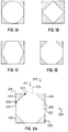
- FIGURES 1A-1D and TABLE A As a example of the light which can potentially be lost from a pixel, refer to FIGURES 1A-1D and TABLE A. From FIGURE 1A and TABLE A, it is seen that a circular lens inscribed within a square pixel and occupying the maximum possible area will be unable to collect approximately 21.5% of the incident light due to the inability of the circular cross-section of the microlens to cover the corners of the pixel. Referring to TABLE A, the square collection area of FIGURE 1B, the hexagon collection area of FIGURE 1C, and the octagon collection area of FIGURE 1D respectively lose approximately 50%, 35.1%, and 17.2% of the light incident upon their corner areas. The particular geometries of FIGURES 1A-1D were chosen for illustrative purposes.
- Representative embodiments of the light sensors described in the present patent document provide enhanced-light-collection capabilities not previously available. Using these teachings, it is possible to collect essentially all of the incident light, a capability that is especially advantageous for image sensors operating in low light intensity situations.
- an enhanced-light-collection-efficiency sensor comprises a pixel and an enhanced-light-collection-efficiency microlens.
- the enhanced-light-collection-efficiency microlens is placed between the pixel and a light or image source.
- the pixel of the light sensor comprises a light-detection area and a non-light-detection area.
- the non-light-detection area does not contribute directly to light detection, but may contain electronic circuitry, interconnecting metal traces, and areas used for isolating the light-detection area of the light sensor. This non-light-detection area is often covered with metal in order to protect underlying electronic structures or electronic circuitry from the effects of the light incident from the light source or image.
- the light-detection area typically has a polygon shaped perimeter and lies within or, at most, touching a pixel typically of rectangular arc.
- the microlens in this representative embodiment comprises one or more corner microlenses located in the corner areas of the pixel. The light incident upon these corner microlenses is refracted at the corner microlens surface from the non-light-detection area onto the light-detection area.
- a light-transmitting microlens is located over the light-detection area and between it and the light source.
- the surface of the light-transmitting microlens which faces the light source collects any light which would otherwise be incident upon the light-detection area and simply transmits or refracts that light onto any part of the light-detection area.
- the light-transmitting microlens may be nothing more than a flat light-transmitting material.
- Representative embodiments of the invention also may be implemented using various polygon cross-sectional shapes perpendicular to the line of light propagation for the light-detection areas. These various polygon shapes consist of, but are not limited to, triangles, squares, pentagons, hexagons, heptagons, octagons, nonagons, decagons, undecagons, and dodecagons. However, other embodiments are possible, and the embodiments of the present patent document are not limited to these geometries. In addition, representative embodiments of individual light sensors, as taught in the present patent document, may be combined into linear and area arrays.
- Embodiments described in the present patent document do not depend upon whether or not the incident light is received directly from an active light source or is reflected from a image.
- the term light source as used herein, is synonymous with image source.
- pixel geometries are described in the present patent document as squares or rectangles. It is noted that a square is, in fact, a special case of a rectangle wherein all sides are equal. While pixels in image sensors are typically rectangles, or squares in the special case of a rectangle of equal sides, embodiments of the present patent document are not limited to such pixel geometries.
- solid-state image sensors such as charged coupled devices (CCD's), complementary metal-oxide-semiconductor (CMOS), and other solid-state electronic devices are required to detect low or marginal light intensities. In these instances, even small losses in detectable light are of significant importance.
- CCD charged coupled devices
- CMOS complementary metal-oxide-semiconductor
- any associated electronic circuitry that may be used for amplifying the light signal may be placed in the corner areas of the pixels, or any other convenient places either within or external to the pixels.
- teachings of the present patent document provide the ability to collect essentially all of the light incident upon the pixels in an image sensor or other light sensitive device.
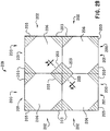
- FIGURE 2A is a top view of a representative embodiment of an enhanced-light-collection-efficiency sensor 200 of the present patent document.
- An enhanced-light-collection-efficiency microlens 202 is inscribed within a pixel 201 .
- the enhanced-light-collection-efficiency microlens 202 comprises a corner microlens 203 in each of the four corners of the pixel 201 and a light-transmitting microlens 206 . While other geometries are possible, the light-transmitting microlens 206 for this embodiment has an octagon shape.
- FIGURE 2B is a top view of an enhanced-light-collection-efficiency sensor array 209 comprising four enhanced-light-collection-efficiency sensors 200 in four adjacent pixels 201 .
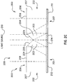
- FIGURE 2C is a drawing of a section of the enhanced-light-collection-efficiency sensor array 209 on line A-A of FIGURE 2B.
- a part of the light from a light source 210 is shown incident upon two adjacent enhanced-light-collection-efficiency sensors 200 of the enhanced-light-collection-efficiency sensor array 209 .
- the enhanced-light-collection-efficiency microlens 202 comprises the corner microlens 203 and the light-transmitting microlens 206 .
- the corner microlens 203 is comprised of a corner microlens body 204 with a corner microlens surface 205 facing the light source 210 .
- the light-transmitting microlens 206 is comprised of a light-transmitting microlens body 207 with a light-transmitting microlens surface 208 facing the light source 210 . Both the corner microlens 203 and the light-transmitting microlens 206 are fabricated from light-transmitting materials.
- the light from the light source 210 is shown incident upon corner microlens surfaces 205 of two adjacent corner microlenses 203 . Light, which would otherwise be incident upon a non-light-detection area 214 of the pixel 201 , is refracted onto a light-detection area 212 of the pixel 201 . Note that FIGURES 2A-2C are drawn neglecting any isolation region between the light-detection areas 212 of adjacent pixels 201 . Light incident upon these isolation regions may be collected by extending the corner microlenses 203 to include such areas.
- the light-transmitting microlens 206 of the enhanced-light-collection efficiency microlens 202 may simply transmit the light incident on it to the light-detection area 212 without refraction by constructing it of a flat sheet of optically transparent material.
- any form of refraction, such as magnification or dispersion, by the light-transmitting microlens 206 also follows the teachings of the present patent document, so long as substantially all of the light incident on the light-transmitting microlens 206 is incident on the light-detection area 212 .
- the light-detection area 212 has a polygon shaped geometry and the perimeter of the light-detection area 212 intersects the perimeter of the pixel 201 .
- the corner microlens 203 for this embodiment is bounded by a vertex 218 of the pixel 201 , a first nearest point 220 , and a second nearest point 222 .
- the first nearest point 220 is chosen by first determining the set of all points on the perimeter of the light-detection area 212 nearest a first adjacent side 224 wherein the first adjacent side 224 is one of the sides of the pixel 201 which intersects the vertex 218 .
- the set of all points on the perimeter of the light-detection area 212 nearest the first adjacent side 224 for this drawing is the line segment in which the light-detection area 212 intersects the first adjacent side 224 .
- the point closest to the vertex 218 is defined to be the first nearest point 220 .
- the second nearest point 222 is chosen in a similar manner by first determining the set of all points on the perimeter of the light-detection area 212 nearest a second adjacent side 226 wherein the second adjacent side 226 is the other side of the pixel 201 which intersects the vertex 218 .
- the set of all points on the perimeter of the light-detection area 212 nearest the second adjacent side 226 for this drawing is the line segment in which the light-detection area 212 intersects the second adjacent side 226 .
- the point closest to the vertex 218 is defined to be the second nearest point 222 .
- FIGURES 3A-3B are drawings of another representative embodiment of the teachings of the present patent document wherein the perimeter of a light-detection arm 312 is formed by first constructing a square whose sides are substantially parallel to a pixel 301 and then removing corner areas from that square. A corner microlens 303 is located over each of the cut-out areas of the light-detection areas 312 .
- Four enhanced-light-collection-efficiency sensors 300 are combined to form an enhanced-light-collection-efficiency sensor array 309 .
- FIGURE 3A is a drawing of a top view of this configuration while FIGURE 3B is a three dimensional sketch of a combination of four adjacent corner microlenses 303 defined, in part, by vertices 352 , 354 , 356 , 358 .
- four adjacent light-detection areas 312 are indicated as 362 , 364 , 366 , 368 .
- corner microlens surfaces 308 of the corner microlenses 303 refract light onto the light-detection areas 312 of four adjacent pixels 301 .
- the four facets of the adjacent microlenses refract light onto the light-detection areas 312 of four adjacent pixels 301 as indicated by the arrows in FIGURE 3A.
- the cross-sectional shape of the light-detection area 212 , 312 could be any regular or irregular polygon such as, but not limited to, a triangle, a square, a rectangle, a pentagon, a hexagon, a heptagon, a octagon, a nonagon, a decagon, a undecagon, a dodecagon, or for that matter it could be any cross-sectional geometry including curved and circular shapes.
- FIGURE 4 is a top view of another representative embodiment of a enhanced-light-collection-efficiency sensor 400 wherein a light-detection area 412 has a circular geometry with a perimeter which does not intersect the perimeter of a pixel 401.
- a corner microlens 403 for this embodiment is bounded as specified in the following.
- a first adjacent side 424 is identified wherein the first adjacent side 424 is one of the two sides of the pixel 401 which intersects a vertex 418 of the pixel 401 .
- a first nearest point 420 is chosen to be the mid-point of the projection onto the first adjacent side 424 of the set of all points on the perimeter of the light-detection area 412 closest to the first adjacent side 424 . Since in this embodiment, there is only one point on the perimeter of the light-detection area 412 that is closest to the first adjacent side 424 , this mid-point is chosen from a set of points consisting of only a single point.
- a second adjacent side 426 is identified wherein the second adjacent side 426 is the second of the two sides of the pixel 401 which intersects the vertex 418 .
- a second nearest point 422 is chosen to be the mid-point of the projection onto the second adjacent side 426 of the set of all points on the perimeter of the light-detection area 412 closest to the second adjacent side 426 .
- this mid-point is chosen from a set of points consisting of only a single point.
- the corner microlens 403 is bounded by the vertex 418 , the first nearest point 420 , the second nearest point 422 , a first projection point 428 which is the projection of the first nearest point 420 onto the perimeter of the light-detection area 412 , a second projection point 430 which is the projection of the second nearest point 422 onto the perimeter of the light-detection area 412 , and the perimeter of the light-detection area 412 lying between the first projection point 428 and the second projection point 430 .
- the curvature and vertical placement of the corner microlens 403 is defined so as to refract substantially all of the light incident on the corner microlens 403 onto the light-detection area 412 .
- a light-transmitting microlens 406 may also be placed over the light-detection area 412 as in other representative embodiments discussed above.
- Embodiments of the microlens of the present patent document, as described herein, are especially useful in applications wherein the level of light detected is marginal with respect to that needed for accurate and reliable detection. In such situations, the loss of even small losses of light is critical.
Landscapes
- Physics & Mathematics (AREA)
- General Physics & Mathematics (AREA)
- Optics & Photonics (AREA)
- Solid State Image Pick-Up Elements (AREA)
- Light Receiving Elements (AREA)
- Transforming Light Signals Into Electric Signals (AREA)
Applications Claiming Priority (2)
| Application Number | Priority Date | Filing Date | Title |
|---|---|---|---|
| US08/893,020 US5903039A (en) | 1997-07-15 | 1997-07-15 | Enhanced-light-collection-efficiency sensor |
| US893020 | 1997-07-15 |
Publications (2)
| Publication Number | Publication Date |
|---|---|
| EP0892287A2 true EP0892287A2 (de) | 1999-01-20 |
| EP0892287A3 EP0892287A3 (de) | 2000-03-08 |
Family
ID=25400892
Family Applications (1)
| Application Number | Title | Priority Date | Filing Date |
|---|---|---|---|
| EP98104192A Withdrawn EP0892287A3 (de) | 1997-07-15 | 1998-03-09 | Bildsensor erhöhter Lichtausbeute mit Mikrolinsenraster |
Country Status (4)
| Country | Link |
|---|---|
| US (1) | US5903039A (de) |
| EP (1) | EP0892287A3 (de) |
| JP (1) | JP4285711B2 (de) |
| TW (1) | TW408230B (de) |
Cited By (2)
| Publication number | Priority date | Publication date | Assignee | Title |
|---|---|---|---|---|
| WO2005053036A1 (en) * | 2003-11-21 | 2005-06-09 | Eastman Kodak Company | Large pixel micro-lens |
| WO2018084328A1 (ko) * | 2016-11-01 | 2018-05-11 | 이호덕 | 마이크로렌즈 어레이 필름 |
Families Citing this family (4)
| Publication number | Priority date | Publication date | Assignee | Title |
|---|---|---|---|---|
| CN100570877C (zh) * | 2005-07-08 | 2009-12-16 | 株式会社尼康 | 固态成像传感器 |
| US8713845B1 (en) * | 2006-08-01 | 2014-05-06 | Raytheon Canada Limited | Method and apparatus for efficiently collecting radiation |
| TWI413242B (zh) * | 2007-08-10 | 2013-10-21 | Hon Hai Prec Ind Co Ltd | 固態圖像感測器 |
| KR20100074443A (ko) * | 2008-12-24 | 2010-07-02 | 주식회사 동부하이텍 | 이미지 센서의 마이크로 렌즈 마스크 및 마이크로 렌즈 형성 방법 |
Family Cites Families (11)
| Publication number | Priority date | Publication date | Assignee | Title |
|---|---|---|---|---|
| GB152556A (en) * | 1920-01-07 | 1920-10-21 | Scotts Shipbuilding And Engine | Improvements in magnetic clutches |
| JPS6047472A (ja) * | 1983-08-26 | 1985-03-14 | Hitachi Ltd | 固体撮像素子 |
| JPS60140879A (ja) * | 1983-12-28 | 1985-07-25 | Fujitsu Ltd | 半導体装置 |
| DE3429812C1 (de) * | 1984-08-14 | 1986-04-10 | Messerschmitt-Bölkow-Blohm GmbH, 8012 Ottobrunn | Monolithischer Bildaufnehmer |
| US4689291A (en) * | 1985-08-30 | 1987-08-25 | Xerox Corporation | Pedestal-type microlens fabrication process |
| US4882262A (en) * | 1987-09-28 | 1989-11-21 | Honeywell Inc. | Self-aligning aperture |
| JPH0264501A (ja) * | 1988-08-30 | 1990-03-05 | Sharp Corp | マイクロレンズアレイ及びその製造方法 |
| US5298366A (en) * | 1990-10-09 | 1994-03-29 | Brother Kogyo Kabushiki Kaisha | Method for producing a microlens array |
| KR950002410A (ko) * | 1993-06-30 | 1995-01-04 | 김광호 | 고체 촬상 장치 |
| JPH08107194A (ja) * | 1994-10-03 | 1996-04-23 | Fuji Photo Optical Co Ltd | 固体撮像装置 |
| WO1997009743A1 (en) * | 1995-09-07 | 1997-03-13 | The Whitaker Corporation | Pin photodiode having elliptical detector area |
-
1997
- 1997-07-15 US US08/893,020 patent/US5903039A/en not_active Expired - Lifetime
-
1998
- 1998-03-09 EP EP98104192A patent/EP0892287A3/de not_active Withdrawn
- 1998-07-01 JP JP18632998A patent/JP4285711B2/ja not_active Expired - Lifetime
- 1998-08-04 TW TW087111518A patent/TW408230B/zh not_active IP Right Cessation
Cited By (2)
| Publication number | Priority date | Publication date | Assignee | Title |
|---|---|---|---|---|
| WO2005053036A1 (en) * | 2003-11-21 | 2005-06-09 | Eastman Kodak Company | Large pixel micro-lens |
| WO2018084328A1 (ko) * | 2016-11-01 | 2018-05-11 | 이호덕 | 마이크로렌즈 어레이 필름 |
Also Published As
| Publication number | Publication date |
|---|---|
| JP4285711B2 (ja) | 2009-06-24 |
| EP0892287A3 (de) | 2000-03-08 |
| TW408230B (en) | 2000-10-11 |
| JPH1197661A (ja) | 1999-04-09 |
| US5903039A (en) | 1999-05-11 |
Similar Documents
| Publication | Publication Date | Title |
|---|---|---|
| JP3462736B2 (ja) | 固体撮像素子 | |
| KR101518744B1 (ko) | 광학식 검지 장치 및 이것을 이용한 기기 | |
| EP1213764B1 (de) | Festkörpersbildsensoren und Mikrolensmatrizen | |
| CN111108511A (zh) | 指纹检测装置和电子设备 | |
| EP0929050A3 (de) | Abtastfähiger Halbleiterfingerabdrukdetektor | |
| US5903039A (en) | Enhanced-light-collection-efficiency sensor | |
| US20160146981A1 (en) | Optical element array and solid-state imaging device including the array | |
| US3923382A (en) | Multifaceted mirror structure for infrared radiation detector | |
| KR102827127B1 (ko) | 이미지 센서 및 이를 포함하는 전자 장치 | |
| CN210605739U (zh) | 指纹检测装置和电子设备 | |
| JP4884465B2 (ja) | ピクセルアレイ上の非対称マイクロレンズ | |
| EP1001283A1 (de) | Optisches element,abbildeeinheit,abbildevorrichtung,strahlungsabbildungssensor und fingerabdruckanalysator unter verwendung derselben | |
| EP0126776A4 (de) | Gerät zur prüfung der eindruckhärte. | |
| EP0547697A3 (de) | Festkörperbildaufnahmeeinrichtung und Kamera mit einer derartigen Bildaufnahmeeinrichtung | |
| JPH11355510A (ja) | 光電性チップ | |
| US5149955A (en) | Full contact image sensor device with light blocking means | |
| EP0543537A2 (de) | Photodetektor mit reduzierter blinder Zone | |
| JP3477729B2 (ja) | ドーム型マルチレンズ | |
| JPH1197661A5 (de) | ||
| JP2520211B2 (ja) | 触覚センサ | |
| CN218772251U (zh) | 集成式放大成像组件及集成式图像采集设备 | |
| US20250267969A1 (en) | Image sensor | |
| JPH04252579A (ja) | 固体撮像装置 | |
| JPH07226884A (ja) | 固体撮像装置 | |
| JPH01106290A (ja) | ウェハー枚数計数装置 |
Legal Events
| Date | Code | Title | Description |
|---|---|---|---|
| PUAI | Public reference made under article 153(3) epc to a published international application that has entered the european phase |
Free format text: ORIGINAL CODE: 0009012 |
|
| AK | Designated contracting states |
Kind code of ref document: A2 Designated state(s): DE FR GB |
|
| AX | Request for extension of the european patent |
Free format text: AL;LT;LV;MK;RO;SI |
|
| PUAL | Search report despatched |
Free format text: ORIGINAL CODE: 0009013 |
|
| AK | Designated contracting states |
Kind code of ref document: A3 Designated state(s): AT BE CH DE DK ES FI FR GB GR IE IT LI LU MC NL PT SE |
|
| AX | Request for extension of the european patent |
Free format text: AL;LT;LV;MK;RO;SI |
|
| RIC1 | Information provided on ipc code assigned before grant |
Free format text: 7G 02B 3/00 A, 7H 01L 31/0232 B |
|
| 17P | Request for examination filed |
Effective date: 20000508 |
|
| 17Q | First examination report despatched |
Effective date: 20000728 |
|
| AKX | Designation fees paid |
Free format text: DE FR GB |
|
| RAP1 | Party data changed (applicant data changed or rights of an application transferred) |
Owner name: HEWLETT-PACKARD COMPANY, A DELAWARE CORPORATION |
|
| STAA | Information on the status of an ep patent application or granted ep patent |
Free format text: STATUS: THE APPLICATION HAS BEEN WITHDRAWN |
|
| 18W | Application withdrawn |
Withdrawal date: 20020502 |