EP0891128A1 - Leiterplatte - Google Patents
Leiterplatte Download PDFInfo
- Publication number
- EP0891128A1 EP0891128A1 EP98305442A EP98305442A EP0891128A1 EP 0891128 A1 EP0891128 A1 EP 0891128A1 EP 98305442 A EP98305442 A EP 98305442A EP 98305442 A EP98305442 A EP 98305442A EP 0891128 A1 EP0891128 A1 EP 0891128A1
- Authority
- EP
- European Patent Office
- Prior art keywords
- elements
- boards
- circuit boards
- spine
- circuit board
- Prior art date
- Legal status (The legal status is an assumption and is not a legal conclusion. Google has not performed a legal analysis and makes no representation as to the accuracy of the status listed.)
- Withdrawn
Links
Images


Classifications
-
- H—ELECTRICITY
- H05—ELECTRIC TECHNIQUES NOT OTHERWISE PROVIDED FOR
- H05K—PRINTED CIRCUITS; CASINGS OR CONSTRUCTIONAL DETAILS OF ELECTRIC APPARATUS; MANUFACTURE OF ASSEMBLAGES OF ELECTRICAL COMPONENTS
- H05K1/00—Printed circuits
- H05K1/02—Details
- H05K1/14—Structural association of two or more printed circuits
- H05K1/148—Arrangements of two or more hingeably connected rigid printed circuit boards, i.e. connected by flexible means
-
- H—ELECTRICITY
- H05—ELECTRIC TECHNIQUES NOT OTHERWISE PROVIDED FOR
- H05K—PRINTED CIRCUITS; CASINGS OR CONSTRUCTIONAL DETAILS OF ELECTRIC APPARATUS; MANUFACTURE OF ASSEMBLAGES OF ELECTRICAL COMPONENTS
- H05K1/00—Printed circuits
- H05K1/02—Details
- H05K1/14—Structural association of two or more printed circuits
- H05K1/144—Stacked arrangements of planar printed circuit boards
-
- H—ELECTRICITY
- H05—ELECTRIC TECHNIQUES NOT OTHERWISE PROVIDED FOR
- H05K—PRINTED CIRCUITS; CASINGS OR CONSTRUCTIONAL DETAILS OF ELECTRIC APPARATUS; MANUFACTURE OF ASSEMBLAGES OF ELECTRICAL COMPONENTS
- H05K2201/00—Indexing scheme relating to printed circuits covered by H05K1/00
- H05K2201/10—Details of components or other objects attached to or integrated in a printed circuit board
- H05K2201/10613—Details of electrical connections of non-printed components, e.g. special leads
- H05K2201/10742—Details of leads
- H05K2201/10886—Other details
- H05K2201/10924—Leads formed from a punched metal foil
Definitions
- This invention relates to an assembly of printed circuit boards of the type in which a pair of circuit boards are mounted parallel to one another with electrical/electronic components mounted upon both sides of the assembly.
- German Patent Application 3842572 discloses a circuit board construction where first and second circuit boards are electrically interconnected by connector device consisting of a plurality of conductive connector elements secured together in electrically insulated relationship by a moulded plastic body, the elements, after being connected to the circuit boards, being bent to allow the boards to overlie one another, the teaching being to provide a specially moulded body to hold the elements in position relative to one another after they have been severed from an integral interconnecting member.
- a circuit board assembly comprising first and second circuit boards arranged parallel to each other, and comb connector means having a plurality of conductive connector elements providing a connection between conducting tracks adjacent an edge of the first circuit board and conducting tracks adjacent an edge of the second board; said plurality of conductive elements of said comb connector originally having been interconnected by an integral spine, the spine being broken in at least one place to isolate one or more conductive elements from adjacent elements after the elements have been secured to the boards.
- the invention also relates to a method of assembling a printed circuit board assembly comprising the steps of providing first and second circuit boards, electrically connecting the circuit boards to one another using a comb connector comprising a plurality of conductive connecting elements interconnected by a spine, mounting components upon the circuit boards whilst the circuit boards are oriented in a substantially coplanar manner, bending the connecting elements of the comb connector until the boards are substantially parallel to one another, and breaking the spine in at least one place to isolate one or more of the elements of the comb connector from adjacent elements thereof.
- said components and the connecting elements of the comb connector are electrically connected to tracks of the circuit boards by a flow soldering technique.
- said spine is broken after bending of the connecting elements to position the boards parallel.
- a comb connector in providing the electrical connection between the boards is advantageous in that as the boards are substantially coplanar, a flow soldering technique can be used to mount the components thereon, the boards subsequently being moved to lie substantially parallel to one another by bending the conductive elements of the comb connector, the elements being held in position relative to one another by their spine prior to connection to the tracks of the boards.
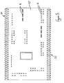
- FIG. 1 illustrates a circuit board assembly which comprises an upper printed circuit board 10 of substantially conventional form and a pair of lower printed circuit boards 12, 14 also of substantially conventional form.
- the upper circuit board 10 carries a plurality of electronic and electrical components 16, some of which take the form of terminal pins arranged to be received by corresponding connectors.
- Each of the components 16 includes one or more terminals which extend through openings provided in the upper circuit board 10, the terminals being electrically connected to conductive tracks printed upon the lower surface of the upper circuit board 10.
- Figures 4 and 5 illustrate that the lower surfaces of the lower circuit boards 12, 14 each carry a plurality of terminal clips 18 for use in supporting fuses.
- the terminal clips 18 each include a terminal which extends through a respective opening provided in the respective lower circuit board, and is soldered to electrically conductive tracks which are printed upon the upper surfaces of the lower printed circuit boards 12, 14.
- the upper and lower circuit boards 10, 12, 14 are electrically connected to one another by means of comb connectors 20 each of which is stamped or otherwise formed from metal strip and includes a plurality of U-shaped connector elements 21 each having a pair of parallel legs, the elements being initially integral with one another by way of a spine 22 of the strip interconnecting the bases of the U-shaped elements.
- each comb connector can be handled as a unitary device.
- Each element of each comb connector has one leg of its pair electrically connected to the printed circuit of the upper board 10 whilst the other leg of each pair is electrically connected to the circuits of one of the lower boards 12, 14. It will be appreciated, therefore, that the comb connectors 20 provide electrical connections between the components 16 provided on the upper circuit board 10 and the fuse terminal clips 18 provided on the lower circuit board 12, 14.
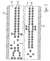
- Figure 2 illustrates a step in the assembly of the circuit board arrangement of Figures 1 and 3 to 5.
- the circuit boards 10, 12, 14 are arranged in a substantially coplanar orientation, the comb connectors 20 providing electrical connections between the printed circuits of the circuit boards.
- the pairs of legs of each comb connector 20 are interconnected by the spine 22.
- the electrical or electronic components 16 and fuse terminal clips 18 are mounted in the appropriate positions upon the circuit boards 10, 12, 14 and are soldered to the electrically conductive tracks of the circuit boards 10, 12, 14 using a flow soldering technique, such a technique only being possible whilst the circuit boards are substantially coplanar.
- an appropriate heat sink arrangement may be located between the upper circuit board and the lower circuit boards.
- the lower circuit boards 12, 14 together are of substantially equal area to that of the upper circuit board 10. It will be appreciated however that the invention is applicable to other circuit board arrangements, for example where only a single lower circuit board is provided, that circuit board being of area substantially equal to the area of the upper circuit board. In such an arrangement, only a single comb connector would be required. In another example, four lower circuit boards are used, each lower circuit board being electrically connected to an edge of the upper circuit board by an associated comb connector which extends along substantially the complete width of the respective edge of the upper board. The lower boards are conveniently of triangular form. The use of this arrangement is advantageous in that an increased number of connections can be made between the upper and lower boards.
Landscapes
- Engineering & Computer Science (AREA)
- Microelectronics & Electronic Packaging (AREA)
- Combinations Of Printed Boards (AREA)
- Coupling Device And Connection With Printed Circuit (AREA)
Applications Claiming Priority (2)
| Application Number | Priority Date | Filing Date | Title |
|---|---|---|---|
| GBGB9714558.5A GB9714558D0 (en) | 1997-07-11 | 1997-07-11 | Circuit board |
| GB9714558 | 1997-07-11 |
Publications (1)
| Publication Number | Publication Date |
|---|---|
| EP0891128A1 true EP0891128A1 (de) | 1999-01-13 |
Family
ID=10815661
Family Applications (1)
| Application Number | Title | Priority Date | Filing Date |
|---|---|---|---|
| EP98305442A Withdrawn EP0891128A1 (de) | 1997-07-11 | 1998-07-08 | Leiterplatte |
Country Status (2)
| Country | Link |
|---|---|
| EP (1) | EP0891128A1 (de) |
| GB (1) | GB9714558D0 (de) |
Cited By (1)
| Publication number | Priority date | Publication date | Assignee | Title |
|---|---|---|---|---|
| DE19912519A1 (de) * | 1999-03-19 | 2000-11-16 | Siemens Ag | Verfahren zum elektrischen Verbinden von Leiterplatten und Leiterplattenanordnung |
Citations (4)
| Publication number | Priority date | Publication date | Assignee | Title |
|---|---|---|---|---|
| CH538798A (de) * | 1971-11-12 | 1973-06-30 | Landis & Gyr Ag | Selbsttragende Leiterplattenanordnung, insbesondere für elektronische Regelgeräte |
| US3893235A (en) * | 1972-11-17 | 1975-07-08 | Texas Instruments Inc | Keyboard electronic apparatus and method of making |
| DE3042585A1 (de) * | 1980-11-12 | 1982-06-16 | SWF-Spezialfabrik für Autozubehör Gustav Rau GmbH, 7120 Bietigheim-Bissingen | Elektrisches geraet, insbesondere fuer kraftfahrzeuge |
| DE3842572A1 (de) * | 1988-12-17 | 1990-06-21 | Bosch Gmbh Robert | Verfahren zum herstellen eines loetkamms fuer das elektrische und mechanische verbinden von leiterplatten |
-
1997
- 1997-07-11 GB GBGB9714558.5A patent/GB9714558D0/en active Pending
-
1998
- 1998-07-08 EP EP98305442A patent/EP0891128A1/de not_active Withdrawn
Patent Citations (4)
| Publication number | Priority date | Publication date | Assignee | Title |
|---|---|---|---|---|
| CH538798A (de) * | 1971-11-12 | 1973-06-30 | Landis & Gyr Ag | Selbsttragende Leiterplattenanordnung, insbesondere für elektronische Regelgeräte |
| US3893235A (en) * | 1972-11-17 | 1975-07-08 | Texas Instruments Inc | Keyboard electronic apparatus and method of making |
| DE3042585A1 (de) * | 1980-11-12 | 1982-06-16 | SWF-Spezialfabrik für Autozubehör Gustav Rau GmbH, 7120 Bietigheim-Bissingen | Elektrisches geraet, insbesondere fuer kraftfahrzeuge |
| DE3842572A1 (de) * | 1988-12-17 | 1990-06-21 | Bosch Gmbh Robert | Verfahren zum herstellen eines loetkamms fuer das elektrische und mechanische verbinden von leiterplatten |
Cited By (2)
| Publication number | Priority date | Publication date | Assignee | Title |
|---|---|---|---|---|
| DE19912519A1 (de) * | 1999-03-19 | 2000-11-16 | Siemens Ag | Verfahren zum elektrischen Verbinden von Leiterplatten und Leiterplattenanordnung |
| DE19912519C2 (de) * | 1999-03-19 | 2001-05-31 | Siemens Ag | Verfahren zum elektrischen Verbinden von Leiterplatten |
Also Published As
| Publication number | Publication date |
|---|---|
| GB9714558D0 (en) | 1997-09-17 |
Similar Documents
| Publication | Publication Date | Title |
|---|---|---|
| EP1168513A1 (de) | Verbindungsstruktur für Leiterplatten und Methode zur Verbindung von einer Leiterplatte | |
| US4835345A (en) | Printed wiring board having robber pads for excess solder | |
| US7247031B2 (en) | Electric junction box and its assembling process | |
| EP1035759A2 (de) | Randmontierbare integrierte Schaltungspackung und Verfahren zu deren Befestigung an einer Leiterplatte | |
| US4343084A (en) | Method for making printed circuit boards with connector terminals | |
| US5112230A (en) | Reconfigurable substrate for electric circuit connections | |
| EP0838101A1 (de) | Elektrische verbinder | |
| EP0303873B1 (de) | Vorrichtung einer leitenden Verbindung | |
| US5525763A (en) | Printed circuit board arrangement | |
| JPH01310598A (ja) | 電子回路用ハウジング | |
| US5753971A (en) | Power semiconductor module with terminal pins | |
| JP2001217025A (ja) | Pcbの終端アダプタ | |
| US4700880A (en) | Process for manufacturing electrical equipment utilizing printed circuit boards | |
| US3304468A (en) | Replaceable electronic module for master circuit boards | |
| EP0891128A1 (de) | Leiterplatte | |
| JPH08236895A (ja) | 印刷配線板 | |
| US4518211A (en) | Device for mounting, interconnecting and terminating printed circuits | |
| EP0774799A1 (de) | Verfahren zur Herstellung von flexiblen gedruckten Leiterplatten, insbesondere für Motorfahrzeuge, und dabei hergestellte gedruckte Leiterplatten | |
| JP3515833B2 (ja) | 配線基板 | |
| WO1984001859A1 (en) | Module mounting assembly | |
| JPH08249932A (ja) | フラット・ハーネス | |
| JP2894034B2 (ja) | フレキシブルプリント配線板のクロス配線方法 | |
| JPH05135834A (ja) | 基板間接続コネクタ | |
| JPH024472Y2 (de) | ||
| JPH1079560A (ja) | 段積印刷基板 |
Legal Events
| Date | Code | Title | Description |
|---|---|---|---|
| PUAI | Public reference made under article 153(3) epc to a published international application that has entered the european phase |
Free format text: ORIGINAL CODE: 0009012 |
|
| AK | Designated contracting states |
Kind code of ref document: A1 Designated state(s): AT BE CH CY DE DK ES FI FR GB GR IE IT LI LU MC NL PT SE |
|
| AX | Request for extension of the european patent |
Free format text: AL;LT;LV;MK;RO;SI |
|
| AKX | Designation fees paid | ||
| STAA | Information on the status of an ep patent application or granted ep patent |
Free format text: STATUS: THE APPLICATION IS DEEMED TO BE WITHDRAWN |
|
| 18D | Application deemed to be withdrawn |
Effective date: 19990714 |
|
| REG | Reference to a national code |
Ref country code: DE Ref legal event code: 8566 |