EP0891121A1 - Organic electroluminescent elements - Google Patents
Organic electroluminescent elements Download PDFInfo
- Publication number
- EP0891121A1 EP0891121A1 EP97950436A EP97950436A EP0891121A1 EP 0891121 A1 EP0891121 A1 EP 0891121A1 EP 97950436 A EP97950436 A EP 97950436A EP 97950436 A EP97950436 A EP 97950436A EP 0891121 A1 EP0891121 A1 EP 0891121A1
- Authority
- EP
- European Patent Office
- Prior art keywords
- organic
- layer
- compound
- injecting
- organic compound
- Prior art date
- Legal status (The legal status is an assumption and is not a legal conclusion. Google has not performed a legal analysis and makes no representation as to the accuracy of the status listed.)
- Granted
Links
- 150000001875 compounds Chemical class 0.000 claims abstract description 118
- 150000002894 organic compounds Chemical class 0.000 claims abstract description 48
- 125000003118 aryl group Chemical group 0.000 claims abstract description 24
- -1 aminophenyl group Chemical group 0.000 claims abstract description 18
- 125000000843 phenylene group Chemical group C1(=C(C=CC=C1)*)* 0.000 claims abstract description 18
- 125000001424 substituent group Chemical group 0.000 claims abstract description 15
- 125000001140 1,4-phenylene group Chemical group [H]C1=C([H])C([*:2])=C([H])C([H])=C1[*:1] 0.000 claims abstract description 5
- 125000002030 1,2-phenylene group Chemical group [H]C1=C([H])C([*:1])=C([*:2])C([H])=C1[H] 0.000 claims abstract description 4
- 125000001989 1,3-phenylene group Chemical group [H]C1=C([H])C([*:1])=C([H])C([*:2])=C1[H] 0.000 claims abstract description 4
- 239000000463 material Substances 0.000 abstract description 46
- 239000010408 film Substances 0.000 abstract description 24
- 238000001704 evaporation Methods 0.000 abstract description 15
- 230000008020 evaporation Effects 0.000 abstract description 15
- 239000010409 thin film Substances 0.000 abstract description 15
- 238000000034 method Methods 0.000 abstract description 9
- 239000011368 organic material Substances 0.000 abstract description 7
- 230000003287 optical effect Effects 0.000 abstract description 5
- 238000011161 development Methods 0.000 abstract description 3
- 239000003086 colorant Substances 0.000 abstract description 2
- 239000010410 layer Substances 0.000 description 152
- 230000015572 biosynthetic process Effects 0.000 description 52
- 238000003786 synthesis reaction Methods 0.000 description 46
- REDXJYDRNCIFBQ-UHFFFAOYSA-N aluminium(3+) Chemical compound [Al+3] REDXJYDRNCIFBQ-UHFFFAOYSA-N 0.000 description 33
- YXFVVABEGXRONW-UHFFFAOYSA-N Toluene Chemical compound CC1=CC=CC=C1 YXFVVABEGXRONW-UHFFFAOYSA-N 0.000 description 30
- 238000006243 chemical reaction Methods 0.000 description 23
- 230000006870 function Effects 0.000 description 22
- 238000010586 diagram Methods 0.000 description 18
- 230000003595 spectral effect Effects 0.000 description 18
- 229910052757 nitrogen Inorganic materials 0.000 description 14
- CAMPQFALWQQPAZ-UHFFFAOYSA-N 1-n-(4-methylphenyl)-4-n-[4-[4-(n-[4-(n-(4-methylphenyl)anilino)phenyl]anilino)phenyl]phenyl]-1-n,4-n-diphenylbenzene-1,4-diamine Chemical compound C1=CC(C)=CC=C1N(C=1C=CC(=CC=1)N(C=1C=CC=CC=1)C=1C=CC(=CC=1)C=1C=CC(=CC=1)N(C=1C=CC=CC=1)C=1C=CC(=CC=1)N(C=1C=CC=CC=1)C=1C=CC(C)=CC=1)C1=CC=CC=C1 CAMPQFALWQQPAZ-UHFFFAOYSA-N 0.000 description 12
- 229910052782 aluminium Inorganic materials 0.000 description 12
- ZUOUZKKEUPVFJK-UHFFFAOYSA-N diphenyl Chemical group C1=CC=CC=C1C1=CC=CC=C1 ZUOUZKKEUPVFJK-UHFFFAOYSA-N 0.000 description 12
- 230000008018 melting Effects 0.000 description 11
- 238000002844 melting Methods 0.000 description 11
- 125000001997 phenyl group Chemical group [H]C1=C([H])C([H])=C(*)C([H])=C1[H] 0.000 description 11
- 239000002904 solvent Substances 0.000 description 11
- 239000000758 substrate Substances 0.000 description 11
- XAGFODPZIPBFFR-UHFFFAOYSA-N aluminium Chemical compound [Al] XAGFODPZIPBFFR-UHFFFAOYSA-N 0.000 description 10
- NNBZCPXTIHJBJL-UHFFFAOYSA-N decalin Chemical compound C1CCCC2CCCCC21 NNBZCPXTIHJBJL-UHFFFAOYSA-N 0.000 description 10
- 239000000706 filtrate Substances 0.000 description 10
- 238000002347 injection Methods 0.000 description 10
- 239000007924 injection Substances 0.000 description 10
- 238000004949 mass spectrometry Methods 0.000 description 10
- VLKZOEOYAKHREP-UHFFFAOYSA-N n-Hexane Chemical compound CCCCCC VLKZOEOYAKHREP-UHFFFAOYSA-N 0.000 description 10
- BWHMMNNQKKPAPP-UHFFFAOYSA-L potassium carbonate Chemical compound [K+].[K+].[O-]C([O-])=O BWHMMNNQKKPAPP-UHFFFAOYSA-L 0.000 description 10
- TVIVIEFSHFOWTE-UHFFFAOYSA-K tri(quinolin-8-yloxy)alumane Chemical compound [Al+3].C1=CN=C2C([O-])=CC=CC2=C1.C1=CN=C2C([O-])=CC=CC2=C1.C1=CN=C2C([O-])=CC=CC2=C1 TVIVIEFSHFOWTE-UHFFFAOYSA-K 0.000 description 10
- 230000009477 glass transition Effects 0.000 description 9
- 238000012360 testing method Methods 0.000 description 9
- LFQSCWFLJHTTHZ-UHFFFAOYSA-N Ethanol Chemical compound CCO LFQSCWFLJHTTHZ-UHFFFAOYSA-N 0.000 description 8
- 238000000113 differential scanning calorimetry Methods 0.000 description 8
- VLCPISYURGTGLP-UHFFFAOYSA-N 1-iodo-3-methylbenzene Chemical compound CC1=CC=CC(I)=C1 VLCPISYURGTGLP-UHFFFAOYSA-N 0.000 description 7
- 239000007983 Tris buffer Substances 0.000 description 7
- 238000010521 absorption reaction Methods 0.000 description 7
- 238000000862 absorption spectrum Methods 0.000 description 7
- 125000000217 alkyl group Chemical group 0.000 description 7
- 125000000732 arylene group Chemical group 0.000 description 7
- 125000002080 perylenyl group Chemical group C1(=CC=C2C=CC=C3C4=CC=CC5=CC=CC(C1=C23)=C45)* 0.000 description 7
- 239000000126 substance Substances 0.000 description 7
- 238000007738 vacuum evaporation Methods 0.000 description 7
- XLYOFNOQVPJJNP-UHFFFAOYSA-N water Substances O XLYOFNOQVPJJNP-UHFFFAOYSA-N 0.000 description 7
- 238000001644 13C nuclear magnetic resonance spectroscopy Methods 0.000 description 6
- 238000005160 1H NMR spectroscopy Methods 0.000 description 6
- CSCPPACGZOOCGX-UHFFFAOYSA-N Acetone Chemical compound CC(C)=O CSCPPACGZOOCGX-UHFFFAOYSA-N 0.000 description 6
- VYPSYNLAJGMNEJ-UHFFFAOYSA-N Silicium dioxide Chemical compound O=[Si]=O VYPSYNLAJGMNEJ-UHFFFAOYSA-N 0.000 description 6
- HFACYLZERDEVSX-UHFFFAOYSA-N benzidine Chemical group C1=CC(N)=CC=C1C1=CC=C(N)C=C1 HFACYLZERDEVSX-UHFFFAOYSA-N 0.000 description 6
- 238000001460 carbon-13 nuclear magnetic resonance spectrum Methods 0.000 description 6
- 239000013078 crystal Substances 0.000 description 6
- UKJLNMAFNRKWGR-UHFFFAOYSA-N cyclohexatrienamine Chemical group NC1=CC=C=C[CH]1 UKJLNMAFNRKWGR-UHFFFAOYSA-N 0.000 description 6
- 238000000151 deposition Methods 0.000 description 6
- 230000008021 deposition Effects 0.000 description 6
- 239000012299 nitrogen atmosphere Substances 0.000 description 6
- 229920000123 polythiophene Polymers 0.000 description 6
- 238000000425 proton nuclear magnetic resonance spectrum Methods 0.000 description 6
- 230000006798 recombination Effects 0.000 description 6
- 238000005215 recombination Methods 0.000 description 6
- 239000000741 silica gel Substances 0.000 description 6
- 229910002027 silica gel Inorganic materials 0.000 description 6
- 239000000243 solution Substances 0.000 description 6
- PMZURENOXWZQFD-UHFFFAOYSA-L Sodium Sulfate Chemical compound [Na+].[Na+].[O-]S([O-])(=O)=O PMZURENOXWZQFD-UHFFFAOYSA-L 0.000 description 5
- 150000001412 amines Chemical class 0.000 description 5
- 239000012298 atmosphere Substances 0.000 description 5
- 239000011230 binding agent Substances 0.000 description 5
- 125000004432 carbon atom Chemical group C* 0.000 description 5
- 150000001879 copper Chemical class 0.000 description 5
- 238000004821 distillation Methods 0.000 description 5
- 230000000694 effects Effects 0.000 description 5
- 230000003993 interaction Effects 0.000 description 5
- 239000003446 ligand Substances 0.000 description 5
- 239000012046 mixed solvent Substances 0.000 description 5
- 239000012044 organic layer Substances 0.000 description 5
- 229960003540 oxyquinoline Drugs 0.000 description 5
- 229910000027 potassium carbonate Inorganic materials 0.000 description 5
- 239000000843 powder Substances 0.000 description 5
- MCJGNVYPOGVAJF-UHFFFAOYSA-N quinolin-8-ol Chemical compound C1=CN=C2C(O)=CC=CC2=C1 MCJGNVYPOGVAJF-UHFFFAOYSA-N 0.000 description 5
- 229910052938 sodium sulfate Inorganic materials 0.000 description 5
- 235000011152 sodium sulphate Nutrition 0.000 description 5
- PXXNTAGJWPJAGM-UHFFFAOYSA-N vertaline Natural products C1C2C=3C=C(OC)C(OC)=CC=3OC(C=C3)=CC=C3CCC(=O)OC1CC1N2CCCC1 PXXNTAGJWPJAGM-UHFFFAOYSA-N 0.000 description 5
- BRSRUYVJULRMRQ-UHFFFAOYSA-N 1-phenylanthracene Chemical class C1=CC=CC=C1C1=CC=CC2=CC3=CC=CC=C3C=C12 BRSRUYVJULRMRQ-UHFFFAOYSA-N 0.000 description 4
- 0 C*(C(CC1)=CC=C*1C(C)=N)/C1=C/C=C/*(*C=C)C#CC1 Chemical compound C*(C(CC1)=CC=C*1C(C)=N)/C1=C/C=C/*(*C=C)C#CC1 0.000 description 4
- AZDRQVAHHNSJOQ-UHFFFAOYSA-N alumane Chemical class [AlH3] AZDRQVAHHNSJOQ-UHFFFAOYSA-N 0.000 description 4
- 125000005577 anthracene group Chemical group 0.000 description 4
- 229940027991 antiseptic and disinfectant quinoline derivative Drugs 0.000 description 4
- 125000002029 aromatic hydrocarbon group Chemical group 0.000 description 4
- 230000001276 controlling effect Effects 0.000 description 4
- 238000002425 crystallisation Methods 0.000 description 4
- 230000008025 crystallization Effects 0.000 description 4
- 238000013461 design Methods 0.000 description 4
- 239000007850 fluorescent dye Substances 0.000 description 4
- 239000011521 glass Substances 0.000 description 4
- 229910052751 metal Inorganic materials 0.000 description 4
- 239000002184 metal Substances 0.000 description 4
- IEQIEDJGQAUEQZ-UHFFFAOYSA-N phthalocyanine Chemical compound N1C(N=C2C3=CC=CC=C3C(N=C3C4=CC=CC=C4C(=N4)N3)=N2)=C(C=CC=C2)C2=C1N=C1C2=CC=CC=C2C4=N1 IEQIEDJGQAUEQZ-UHFFFAOYSA-N 0.000 description 4
- 229920000642 polymer Polymers 0.000 description 4
- 230000008569 process Effects 0.000 description 4
- 150000003248 quinolines Chemical class 0.000 description 4
- 239000011347 resin Substances 0.000 description 4
- 229920005989 resin Polymers 0.000 description 4
- GEYOCULIXLDCMW-UHFFFAOYSA-N 1,2-phenylenediamine Chemical group NC1=CC=CC=C1N GEYOCULIXLDCMW-UHFFFAOYSA-N 0.000 description 3
- INLRGHMVXPDBAR-UHFFFAOYSA-N 1-N-(4-methylphenyl)-4-N-[4-(N-[4-[4-(N-[4-(N-[4-(N-(4-methylphenyl)anilino)phenyl]anilino)phenyl]anilino)phenyl]phenyl]anilino)phenyl]-1-N,4-N-diphenylbenzene-1,4-diamine Chemical compound C1=CC(C)=CC=C1N(C=1C=CC(=CC=1)N(C=1C=CC=CC=1)C=1C=CC(=CC=1)N(C=1C=CC=CC=1)C=1C=CC(=CC=1)C=1C=CC(=CC=1)N(C=1C=CC=CC=1)C=1C=CC(=CC=1)N(C=1C=CC=CC=1)C=1C=CC(=CC=1)N(C=1C=CC=CC=1)C=1C=CC(C)=CC=1)C1=CC=CC=C1 INLRGHMVXPDBAR-UHFFFAOYSA-N 0.000 description 3
- XZCGKDKLYXRVOA-UHFFFAOYSA-N 4-N-[4-(N-naphthalen-1-ylanilino)phenyl]-1-N-[4-[4-(N-[4-(N-[4-(N-naphthalen-1-ylanilino)phenyl]anilino)phenyl]anilino)phenyl]phenyl]-1-N,4-N-diphenylbenzene-1,4-diamine Chemical compound C1=CC=CC=C1N(C=1C=CC(=CC=1)N(C=1C=CC=CC=1)C=1C2=CC=CC=C2C=CC=1)C1=CC=C(N(C=2C=CC=CC=2)C=2C=CC(=CC=2)C=2C=CC(=CC=2)N(C=2C=CC=CC=2)C=2C=CC(=CC=2)N(C=2C=CC=CC=2)C=2C=CC(=CC=2)N(C=2C=CC=CC=2)C=2C3=CC=CC=C3C=CC=2)C=C1 XZCGKDKLYXRVOA-UHFFFAOYSA-N 0.000 description 3
- PDWMBTLFELSCJP-UHFFFAOYSA-N 4-n-(3-methylphenyl)-1-n,4-n-diphenylbenzene-1,4-diamine Chemical compound CC1=CC=CC(N(C=2C=CC=CC=2)C=2C=CC(NC=3C=CC=CC=3)=CC=2)=C1 PDWMBTLFELSCJP-UHFFFAOYSA-N 0.000 description 3
- XEKOWRVHYACXOJ-UHFFFAOYSA-N Ethyl acetate Chemical compound CCOC(C)=O XEKOWRVHYACXOJ-UHFFFAOYSA-N 0.000 description 3
- 239000011358 absorbing material Substances 0.000 description 3
- 125000003545 alkoxy group Chemical group 0.000 description 3
- 125000005428 anthryl group Chemical group [H]C1=C([H])C([H])=C2C([H])=C3C(*)=C([H])C([H])=C([H])C3=C([H])C2=C1[H] 0.000 description 3
- 125000006615 aromatic heterocyclic group Chemical group 0.000 description 3
- 125000004104 aryloxy group Chemical group 0.000 description 3
- 235000010290 biphenyl Nutrition 0.000 description 3
- 239000004305 biphenyl Substances 0.000 description 3
- 238000010549 co-Evaporation Methods 0.000 description 3
- 230000000052 comparative effect Effects 0.000 description 3
- 239000006185 dispersion Substances 0.000 description 3
- 238000009826 distribution Methods 0.000 description 3
- 239000002019 doping agent Substances 0.000 description 3
- 238000001035 drying Methods 0.000 description 3
- 239000012535 impurity Substances 0.000 description 3
- 239000011777 magnesium Substances 0.000 description 3
- 229910052749 magnesium Inorganic materials 0.000 description 3
- 238000002156 mixing Methods 0.000 description 3
- 125000002950 monocyclic group Chemical group 0.000 description 3
- 125000001624 naphthyl group Chemical group 0.000 description 3
- 238000007254 oxidation reaction Methods 0.000 description 3
- 125000001725 pyrenyl group Chemical group 0.000 description 3
- YYMBJDOZVAITBP-UHFFFAOYSA-N rubrene Chemical compound C1=CC=CC=C1C(C1=C(C=2C=CC=CC=2)C2=CC=CC=C2C(C=2C=CC=CC=2)=C11)=C(C=CC=C2)C2=C1C1=CC=CC=C1 YYMBJDOZVAITBP-UHFFFAOYSA-N 0.000 description 3
- 125000003107 substituted aryl group Chemical group 0.000 description 3
- QGMMWGLDOBFHTL-UHFFFAOYSA-N 1,4-bis(4-iodophenyl)benzene Chemical group C1=CC(I)=CC=C1C1=CC=C(C=2C=CC(I)=CC=2)C=C1 QGMMWGLDOBFHTL-UHFFFAOYSA-N 0.000 description 2
- GPYDMVZCPRONLW-UHFFFAOYSA-N 1-iodo-4-(4-iodophenyl)benzene Chemical group C1=CC(I)=CC=C1C1=CC=C(I)C=C1 GPYDMVZCPRONLW-UHFFFAOYSA-N 0.000 description 2
- UDHAWRUAECEBHC-UHFFFAOYSA-N 1-iodo-4-methylbenzene Chemical compound CC1=CC=C(I)C=C1 UDHAWRUAECEBHC-UHFFFAOYSA-N 0.000 description 2
- NHPPIJMARIVBGU-UHFFFAOYSA-N 1-iodonaphthalene Chemical compound C1=CC=C2C(I)=CC=CC2=C1 NHPPIJMARIVBGU-UHFFFAOYSA-N 0.000 description 2
- MVWPVABZQQJTPL-UHFFFAOYSA-N 2,3-diphenylcyclohexa-2,5-diene-1,4-dione Chemical class O=C1C=CC(=O)C(C=2C=CC=CC=2)=C1C1=CC=CC=C1 MVWPVABZQQJTPL-UHFFFAOYSA-N 0.000 description 2
- IWTQHJROHBAJSF-UHFFFAOYSA-N 2-n-(3-methylphenyl)-1-n,2-n-diphenylbenzene-1,2-diamine Chemical compound CC1=CC=CC(N(C=2C=CC=CC=2)C=2C(=CC=CC=2)NC=2C=CC=CC=2)=C1 IWTQHJROHBAJSF-UHFFFAOYSA-N 0.000 description 2
- QYNTUCBQEHUHCS-UHFFFAOYSA-N 4-n-(3-methylphenyl)-1-n-[4-[4-(n-[4-(n-(3-methylphenyl)anilino)phenyl]anilino)phenyl]phenyl]-1-n,4-n-diphenylbenzene-1,4-diamine Chemical compound CC1=CC=CC(N(C=2C=CC=CC=2)C=2C=CC(=CC=2)N(C=2C=CC=CC=2)C=2C=CC(=CC=2)C=2C=CC(=CC=2)N(C=2C=CC=CC=2)C=2C=CC(=CC=2)N(C=2C=CC=CC=2)C=2C=C(C)C=CC=2)=C1 QYNTUCBQEHUHCS-UHFFFAOYSA-N 0.000 description 2
- RYGMFSIKBFXOCR-UHFFFAOYSA-N Copper Chemical compound [Cu] RYGMFSIKBFXOCR-UHFFFAOYSA-N 0.000 description 2
- VEXZGXHMUGYJMC-UHFFFAOYSA-N Hydrochloric acid Chemical compound Cl VEXZGXHMUGYJMC-UHFFFAOYSA-N 0.000 description 2
- KWYHDKDOAIKMQN-UHFFFAOYSA-N N,N,N',N'-tetramethylethylenediamine Chemical compound CN(C)CCN(C)C KWYHDKDOAIKMQN-UHFFFAOYSA-N 0.000 description 2
- HCHKCACWOHOZIP-UHFFFAOYSA-N Zinc Chemical compound [Zn] HCHKCACWOHOZIP-UHFFFAOYSA-N 0.000 description 2
- 125000002947 alkylene group Chemical group 0.000 description 2
- 125000003277 amino group Chemical group 0.000 description 2
- 125000002490 anilino group Chemical group [H]N(*)C1=C([H])C([H])=C([H])C([H])=C1[H] 0.000 description 2
- MWPLVEDNUUSJAV-UHFFFAOYSA-N anthracene Chemical compound C1=CC=CC2=CC3=CC=CC=C3C=C21 MWPLVEDNUUSJAV-UHFFFAOYSA-N 0.000 description 2
- 239000012300 argon atmosphere Substances 0.000 description 2
- 125000002529 biphenylenyl group Chemical group C1(=CC=CC=2C3=CC=CC=C3C12)* 0.000 description 2
- 230000000903 blocking effect Effects 0.000 description 2
- 238000009835 boiling Methods 0.000 description 2
- 239000011575 calcium Substances 0.000 description 2
- 229910052791 calcium Inorganic materials 0.000 description 2
- 239000000969 carrier Substances 0.000 description 2
- 230000015556 catabolic process Effects 0.000 description 2
- 239000003054 catalyst Substances 0.000 description 2
- 239000011248 coating agent Substances 0.000 description 2
- 238000000576 coating method Methods 0.000 description 2
- 229910052802 copper Inorganic materials 0.000 description 2
- 239000010949 copper Substances 0.000 description 2
- VPUGDVKSAQVFFS-UHFFFAOYSA-N coronene Chemical compound C1=C(C2=C34)C=CC3=CC=C(C=C3)C4=C4C3=CC=C(C=C3)C4=C2C3=C1 VPUGDVKSAQVFFS-UHFFFAOYSA-N 0.000 description 2
- 230000008878 coupling Effects 0.000 description 2
- 238000010168 coupling process Methods 0.000 description 2
- 238000005859 coupling reaction Methods 0.000 description 2
- 230000007547 defect Effects 0.000 description 2
- 230000032798 delamination Effects 0.000 description 2
- 239000003599 detergent Substances 0.000 description 2
- 230000006866 deterioration Effects 0.000 description 2
- ZBQUMMFUJLOTQC-UHFFFAOYSA-L dichloronickel;3-diphenylphosphanylpropyl(diphenyl)phosphane Chemical compound Cl[Ni]Cl.C=1C=CC=CC=1P(C=1C=CC=CC=1)CCCP(C=1C=CC=CC=1)C1=CC=CC=C1 ZBQUMMFUJLOTQC-UHFFFAOYSA-L 0.000 description 2
- 238000000605 extraction Methods 0.000 description 2
- UYTPUPDQBNUYGX-UHFFFAOYSA-N guanine Chemical compound O=C1NC(N)=NC2=C1N=CN2 UYTPUPDQBNUYGX-UHFFFAOYSA-N 0.000 description 2
- 229910052738 indium Inorganic materials 0.000 description 2
- 229910003437 indium oxide Inorganic materials 0.000 description 2
- PJXISJQVUVHSOJ-UHFFFAOYSA-N indium(iii) oxide Chemical compound [O-2].[O-2].[O-2].[In+3].[In+3] PJXISJQVUVHSOJ-UHFFFAOYSA-N 0.000 description 2
- 238000003475 lamination Methods 0.000 description 2
- 229910052744 lithium Inorganic materials 0.000 description 2
- 238000004519 manufacturing process Methods 0.000 description 2
- VNWKTOKETHGBQD-UHFFFAOYSA-N methane Chemical compound C VNWKTOKETHGBQD-UHFFFAOYSA-N 0.000 description 2
- 125000002496 methyl group Chemical group [H]C([H])([H])* 0.000 description 2
- 230000007935 neutral effect Effects 0.000 description 2
- 238000000655 nuclear magnetic resonance spectrum Methods 0.000 description 2
- 150000004866 oxadiazoles Chemical class 0.000 description 2
- 230000003647 oxidation Effects 0.000 description 2
- 229910052760 oxygen Inorganic materials 0.000 description 2
- 125000005561 phenanthryl group Chemical group 0.000 description 2
- 229920000553 poly(phenylenevinylene) Polymers 0.000 description 2
- 125000003367 polycyclic group Chemical group 0.000 description 2
- 229910052700 potassium Inorganic materials 0.000 description 2
- 150000003222 pyridines Chemical class 0.000 description 2
- 229940083082 pyrimidine derivative acting on arteriolar smooth muscle Drugs 0.000 description 2
- 150000003230 pyrimidines Chemical class 0.000 description 2
- 150000003252 quinoxalines Chemical class 0.000 description 2
- 238000007789 sealing Methods 0.000 description 2
- 239000011734 sodium Substances 0.000 description 2
- LPXPTNMVRIOKMN-UHFFFAOYSA-M sodium nitrite Chemical compound [Na+].[O-]N=O LPXPTNMVRIOKMN-UHFFFAOYSA-M 0.000 description 2
- 238000001228 spectrum Methods 0.000 description 2
- 238000004528 spin coating Methods 0.000 description 2
- 238000003756 stirring Methods 0.000 description 2
- 238000003860 storage Methods 0.000 description 2
- 125000005504 styryl group Chemical group 0.000 description 2
- 238000000859 sublimation Methods 0.000 description 2
- 230000008022 sublimation Effects 0.000 description 2
- XOLBLPGZBRYERU-UHFFFAOYSA-N tin dioxide Chemical compound O=[Sn]=O XOLBLPGZBRYERU-UHFFFAOYSA-N 0.000 description 2
- 125000005259 triarylamine group Chemical group 0.000 description 2
- 229910052725 zinc Inorganic materials 0.000 description 2
- 239000011701 zinc Substances 0.000 description 2
- QGKMIGUHVLGJBR-UHFFFAOYSA-M (4z)-1-(3-methylbutyl)-4-[[1-(3-methylbutyl)quinolin-1-ium-4-yl]methylidene]quinoline;iodide Chemical class [I-].C12=CC=CC=C2N(CCC(C)C)C=CC1=CC1=CC=[N+](CCC(C)C)C2=CC=CC=C12 QGKMIGUHVLGJBR-UHFFFAOYSA-M 0.000 description 1
- UWRZIZXBOLBCON-VOTSOKGWSA-N (e)-2-phenylethenamine Chemical class N\C=C\C1=CC=CC=C1 UWRZIZXBOLBCON-VOTSOKGWSA-N 0.000 description 1
- KLCLIOISYBHYDZ-UHFFFAOYSA-N 1,4,4-triphenylbuta-1,3-dienylbenzene Chemical compound C=1C=CC=CC=1C(C=1C=CC=CC=1)=CC=C(C=1C=CC=CC=1)C1=CC=CC=C1 KLCLIOISYBHYDZ-UHFFFAOYSA-N 0.000 description 1
- LFMWZTSOMGDDJU-UHFFFAOYSA-N 1,4-diiodobenzene Chemical compound IC1=CC=C(I)C=C1 LFMWZTSOMGDDJU-UHFFFAOYSA-N 0.000 description 1
- KAQUBIATNWQNRE-UHFFFAOYSA-N 1-iodo-3-phenylbenzene Chemical group IC1=CC=CC(C=2C=CC=CC=2)=C1 KAQUBIATNWQNRE-UHFFFAOYSA-N 0.000 description 1
- XFYQEBBUVNLYBR-UHFFFAOYSA-N 12-phthaloperinone Chemical class C1=CC(N2C(=O)C=3C(=CC=CC=3)C2=N2)=C3C2=CC=CC3=C1 XFYQEBBUVNLYBR-UHFFFAOYSA-N 0.000 description 1
- QKZFBFSFZILINR-UHFFFAOYSA-N 3-methyl-N-[4-[4-(N-(3-methylphenyl)anilino)phenyl]phenyl]-N-phenylaniline Chemical compound CC=1C=C(C=CC1)N(C1=CC=C(C=C1)C1=CC=C(N(C2=CC=CC=C2)C2=CC(=CC=C2)C)C=C1)C1=CC=CC=C1.CC=1C=C(C=CC1)N(C1=CC=C(C=C1)C1=CC=C(N(C2=CC=CC=C2)C2=CC(=CC=C2)C)C=C1)C1=CC=CC=C1 QKZFBFSFZILINR-UHFFFAOYSA-N 0.000 description 1
- UDQLIWBWHVOIIF-UHFFFAOYSA-N 3-phenylbenzene-1,2-diamine Chemical compound NC1=CC=CC(C=2C=CC=CC=2)=C1N UDQLIWBWHVOIIF-UHFFFAOYSA-N 0.000 description 1
- FDRNXKXKFNHNCA-UHFFFAOYSA-N 4-(4-anilinophenyl)-n-phenylaniline Chemical compound C=1C=C(C=2C=CC(NC=3C=CC=CC=3)=CC=2)C=CC=1NC1=CC=CC=C1 FDRNXKXKFNHNCA-UHFFFAOYSA-N 0.000 description 1
- WDFJQDKZFVQSOT-UHFFFAOYSA-N 4-N-[4-(N-(3-methylphenyl)anilino)phenyl]-1-N-[4-[4-(N-[4-(N-[4-(N-(3-methylphenyl)anilino)phenyl]anilino)phenyl]anilino)phenyl]phenyl]-1-N,4-N-diphenylbenzene-1,4-diamine Chemical compound CC1=CC=CC(N(C=2C=CC=CC=2)C=2C=CC(=CC=2)N(C=2C=CC=CC=2)C=2C=CC(=CC=2)N(C=2C=CC=CC=2)C=2C=CC(=CC=2)C=2C=CC(=CC=2)N(C=2C=CC=CC=2)C=2C=CC(=CC=2)N(C=2C=CC=CC=2)C=2C=CC(=CC=2)N(C=2C=CC=CC=2)C=2C=C(C)C=CC=2)=C1 WDFJQDKZFVQSOT-UHFFFAOYSA-N 0.000 description 1
- QBSMHWVGUPQNJJ-UHFFFAOYSA-N 4-[4-(4-aminophenyl)phenyl]aniline Chemical group C1=CC(N)=CC=C1C1=CC=C(C=2C=CC(N)=CC=2)C=C1 QBSMHWVGUPQNJJ-UHFFFAOYSA-N 0.000 description 1
- UXKQNCDDHDBAPD-UHFFFAOYSA-N 4-n,4-n-diphenylbenzene-1,4-diamine Chemical compound C1=CC(N)=CC=C1N(C=1C=CC=CC=1)C1=CC=CC=C1 UXKQNCDDHDBAPD-UHFFFAOYSA-N 0.000 description 1
- KSSJBGNOJJETTC-UHFFFAOYSA-N COC1=C(C=CC=C1)N(C1=CC=2C3(C4=CC(=CC=C4C=2C=C1)N(C1=CC=C(C=C1)OC)C1=C(C=CC=C1)OC)C1=CC(=CC=C1C=1C=CC(=CC=13)N(C1=CC=C(C=C1)OC)C1=C(C=CC=C1)OC)N(C1=CC=C(C=C1)OC)C1=C(C=CC=C1)OC)C1=CC=C(C=C1)OC Chemical compound COC1=C(C=CC=C1)N(C1=CC=2C3(C4=CC(=CC=C4C=2C=C1)N(C1=CC=C(C=C1)OC)C1=C(C=CC=C1)OC)C1=CC(=CC=C1C=1C=CC(=CC=13)N(C1=CC=C(C=C1)OC)C1=C(C=CC=C1)OC)N(C1=CC=C(C=C1)OC)C1=C(C=CC=C1)OC)C1=CC=C(C=C1)OC KSSJBGNOJJETTC-UHFFFAOYSA-N 0.000 description 1
- OYPRJOBELJOOCE-UHFFFAOYSA-N Calcium Chemical compound [Ca] OYPRJOBELJOOCE-UHFFFAOYSA-N 0.000 description 1
- GYHNNYVSQQEPJS-UHFFFAOYSA-N Gallium Chemical compound [Ga] GYHNNYVSQQEPJS-UHFFFAOYSA-N 0.000 description 1
- FYYHWMGAXLPEAU-UHFFFAOYSA-N Magnesium Chemical compound [Mg] FYYHWMGAXLPEAU-UHFFFAOYSA-N 0.000 description 1
- NRCMAYZCPIVABH-UHFFFAOYSA-N Quinacridone Chemical compound N1C2=CC=CC=C2C(=O)C2=C1C=C1C(=O)C3=CC=CC=C3NC1=C2 NRCMAYZCPIVABH-UHFFFAOYSA-N 0.000 description 1
- 238000006887 Ullmann reaction Methods 0.000 description 1
- 230000009471 action Effects 0.000 description 1
- 125000005036 alkoxyphenyl group Chemical group 0.000 description 1
- 125000005037 alkyl phenyl group Chemical group 0.000 description 1
- 239000000956 alloy Substances 0.000 description 1
- 229910045601 alloy Inorganic materials 0.000 description 1
- 125000004653 anthracenylene group Chemical group 0.000 description 1
- 229940054051 antipsychotic indole derivative Drugs 0.000 description 1
- 239000007864 aqueous solution Substances 0.000 description 1
- 150000004982 aromatic amines Chemical class 0.000 description 1
- 150000004945 aromatic hydrocarbons Chemical class 0.000 description 1
- 150000008378 aryl ethers Chemical class 0.000 description 1
- YCOXTKKNXUZSKD-UHFFFAOYSA-N as-o-xylenol Natural products CC1=CC=C(O)C=C1C YCOXTKKNXUZSKD-UHFFFAOYSA-N 0.000 description 1
- QVGXLLKOCUKJST-UHFFFAOYSA-N atomic oxygen Chemical compound [O] QVGXLLKOCUKJST-UHFFFAOYSA-N 0.000 description 1
- 125000005605 benzo group Chemical group 0.000 description 1
- 125000000609 carbazolyl group Chemical class C1(=CC=CC=2C3=CC=CC=C3NC12)* 0.000 description 1
- 230000008859 change Effects 0.000 description 1
- 238000009833 condensation Methods 0.000 description 1
- 230000005494 condensation Effects 0.000 description 1
- 238000010276 construction Methods 0.000 description 1
- 150000004696 coordination complex Chemical class 0.000 description 1
- 125000000332 coumarinyl group Chemical class O1C(=O)C(=CC2=CC=CC=C12)* 0.000 description 1
- 238000005520 cutting process Methods 0.000 description 1
- 125000000753 cycloalkyl group Chemical group 0.000 description 1
- 230000009849 deactivation Effects 0.000 description 1
- 239000000412 dendrimer Substances 0.000 description 1
- 229920000736 dendritic polymer Polymers 0.000 description 1
- 125000004427 diamine group Chemical group 0.000 description 1
- 150000004985 diamines Chemical class 0.000 description 1
- 239000000975 dye Substances 0.000 description 1
- 230000005684 electric field Effects 0.000 description 1
- 238000000295 emission spectrum Methods 0.000 description 1
- 125000001495 ethyl group Chemical group [H]C([H])([H])C([H])([H])* 0.000 description 1
- 125000000816 ethylene group Chemical group [H]C([H])([*:1])C([H])([H])[*:2] 0.000 description 1
- 125000003983 fluorenyl group Chemical class C1(=CC=CC=2C3=CC=CC=C3CC12)* 0.000 description 1
- 125000001153 fluoro group Chemical class F* 0.000 description 1
- 125000002541 furyl group Chemical group 0.000 description 1
- 229910052733 gallium Inorganic materials 0.000 description 1
- 229910052737 gold Inorganic materials 0.000 description 1
- 150000004820 halides Chemical class 0.000 description 1
- RBTKNAXYKSUFRK-UHFFFAOYSA-N heliogen blue Chemical compound [Cu].[N-]1C2=C(C=CC=C3)C3=C1N=C([N-]1)C3=CC=CC=C3C1=NC([N-]1)=C(C=CC=C3)C3=C1N=C([N-]1)C3=CC=CC=C3C1=N2 RBTKNAXYKSUFRK-UHFFFAOYSA-N 0.000 description 1
- 125000005842 heteroatom Chemical group 0.000 description 1
- 150000002391 heterocyclic compounds Chemical class 0.000 description 1
- 150000007857 hydrazones Chemical class 0.000 description 1
- XMBWDFGMSWQBCA-UHFFFAOYSA-N hydrogen iodide Chemical compound I XMBWDFGMSWQBCA-UHFFFAOYSA-N 0.000 description 1
- 150000002460 imidazoles Chemical class 0.000 description 1
- APFVFJFRJDLVQX-UHFFFAOYSA-N indium atom Chemical compound [In] APFVFJFRJDLVQX-UHFFFAOYSA-N 0.000 description 1
- 150000002475 indoles Chemical class 0.000 description 1
- 229910010272 inorganic material Inorganic materials 0.000 description 1
- 239000011147 inorganic material Substances 0.000 description 1
- 229940079865 intestinal antiinfectives imidazole derivative Drugs 0.000 description 1
- SNHMUERNLJLMHN-UHFFFAOYSA-N iodobenzene Chemical compound IC1=CC=CC=C1 SNHMUERNLJLMHN-UHFFFAOYSA-N 0.000 description 1
- 239000000990 laser dye Substances 0.000 description 1
- 230000031700 light absorption Effects 0.000 description 1
- 230000001795 light effect Effects 0.000 description 1
- 239000007788 liquid Substances 0.000 description 1
- 239000004973 liquid crystal related substance Substances 0.000 description 1
- 239000000434 metal complex dye Substances 0.000 description 1
- 150000002739 metals Chemical class 0.000 description 1
- 125000001570 methylene group Chemical group [H]C([H])([*:1])[*:2] 0.000 description 1
- 230000005012 migration Effects 0.000 description 1
- 238000013508 migration Methods 0.000 description 1
- 239000002052 molecular layer Substances 0.000 description 1
- 229910052759 nickel Inorganic materials 0.000 description 1
- TWNQGVIAIRXVLR-UHFFFAOYSA-N oxo(oxoalumanyloxy)alumane Chemical compound O=[Al]O[Al]=O TWNQGVIAIRXVLR-UHFFFAOYSA-N 0.000 description 1
- 239000001301 oxygen Substances 0.000 description 1
- 229910052763 palladium Inorganic materials 0.000 description 1
- CSHWQDPOILHKBI-UHFFFAOYSA-N peryrene Natural products C1=CC(C2=CC=CC=3C2=C2C=CC=3)=C3C2=CC=CC3=C1 CSHWQDPOILHKBI-UHFFFAOYSA-N 0.000 description 1
- 238000000206 photolithography Methods 0.000 description 1
- 230000000704 physical effect Effects 0.000 description 1
- 229910052697 platinum Inorganic materials 0.000 description 1
- 125000005575 polycyclic aromatic hydrocarbon group Polymers 0.000 description 1
- 238000006116 polymerization reaction Methods 0.000 description 1
- 229920000128 polypyrrole Polymers 0.000 description 1
- 239000002243 precursor Substances 0.000 description 1
- 125000003263 primary aromatic amine group Chemical group 0.000 description 1
- 238000007639 printing Methods 0.000 description 1
- 239000000047 product Substances 0.000 description 1
- 239000011241 protective layer Substances 0.000 description 1
- 125000004076 pyridyl group Chemical group 0.000 description 1
- 125000000168 pyrrolyl group Chemical group 0.000 description 1
- 230000008707 rearrangement Effects 0.000 description 1
- 230000001105 regulatory effect Effects 0.000 description 1
- 150000003336 secondary aromatic amines Chemical class 0.000 description 1
- 229910052709 silver Inorganic materials 0.000 description 1
- 239000002356 single layer Substances 0.000 description 1
- 238000009751 slip forming Methods 0.000 description 1
- 229910052708 sodium Inorganic materials 0.000 description 1
- 235000010288 sodium nitrite Nutrition 0.000 description 1
- 238000001179 sorption measurement Methods 0.000 description 1
- 238000004544 sputter deposition Methods 0.000 description 1
- PMJMHCXAGMRGBZ-UHFFFAOYSA-N subphthalocyanine Chemical class N1C(N=C2C3=CC=CC=C3C(=N3)N2)=C(C=CC=C2)C2=C1N=C1C2=CC=CC=C2C3=N1 PMJMHCXAGMRGBZ-UHFFFAOYSA-N 0.000 description 1
- 229910052717 sulfur Inorganic materials 0.000 description 1
- 239000000725 suspension Substances 0.000 description 1
- 229940042055 systemic antimycotics triazole derivative Drugs 0.000 description 1
- 125000006836 terphenylene group Chemical group 0.000 description 1
- JLZUZNKTTIRERF-UHFFFAOYSA-N tetraphenylethylene Chemical compound C1=CC=CC=C1C(C=1C=CC=CC=1)=C(C=1C=CC=CC=1)C1=CC=CC=C1 JLZUZNKTTIRERF-UHFFFAOYSA-N 0.000 description 1
- 238000005979 thermal decomposition reaction Methods 0.000 description 1
- 125000001544 thienyl group Chemical group 0.000 description 1
- 238000002366 time-of-flight method Methods 0.000 description 1
- ODHXBMXNKOYIBV-UHFFFAOYSA-N triphenylamine Chemical compound C1=CC=CC=C1N(C=1C=CC=CC=1)C1=CC=CC=C1 ODHXBMXNKOYIBV-UHFFFAOYSA-N 0.000 description 1
- 238000001947 vapour-phase growth Methods 0.000 description 1
- 238000005406 washing Methods 0.000 description 1
Images


Classifications
-
- H—ELECTRICITY
- H05—ELECTRIC TECHNIQUES NOT OTHERWISE PROVIDED FOR
- H05B—ELECTRIC HEATING; ELECTRIC LIGHT SOURCES NOT OTHERWISE PROVIDED FOR; CIRCUIT ARRANGEMENTS FOR ELECTRIC LIGHT SOURCES, IN GENERAL
- H05B33/00—Electroluminescent light sources
- H05B33/12—Light sources with substantially two-dimensional radiating surfaces
- H05B33/14—Light sources with substantially two-dimensional radiating surfaces characterised by the chemical or physical composition or the arrangement of the electroluminescent material, or by the simultaneous addition of the electroluminescent material in or onto the light source
-
- C—CHEMISTRY; METALLURGY
- C09—DYES; PAINTS; POLISHES; NATURAL RESINS; ADHESIVES; COMPOSITIONS NOT OTHERWISE PROVIDED FOR; APPLICATIONS OF MATERIALS NOT OTHERWISE PROVIDED FOR
- C09K—MATERIALS FOR MISCELLANEOUS APPLICATIONS, NOT PROVIDED FOR ELSEWHERE
- C09K11/00—Luminescent, e.g. electroluminescent, chemiluminescent materials
- C09K11/06—Luminescent, e.g. electroluminescent, chemiluminescent materials containing organic luminescent materials
-
- H—ELECTRICITY
- H05—ELECTRIC TECHNIQUES NOT OTHERWISE PROVIDED FOR
- H05B—ELECTRIC HEATING; ELECTRIC LIGHT SOURCES NOT OTHERWISE PROVIDED FOR; CIRCUIT ARRANGEMENTS FOR ELECTRIC LIGHT SOURCES, IN GENERAL
- H05B33/00—Electroluminescent light sources
- H05B33/12—Light sources with substantially two-dimensional radiating surfaces
-
- H—ELECTRICITY
- H10—SEMICONDUCTOR DEVICES; ELECTRIC SOLID-STATE DEVICES NOT OTHERWISE PROVIDED FOR
- H10K—ORGANIC ELECTRIC SOLID-STATE DEVICES
- H10K50/00—Organic light-emitting devices
- H10K50/10—OLEDs or polymer light-emitting diodes [PLED]
- H10K50/11—OLEDs or polymer light-emitting diodes [PLED] characterised by the electroluminescent [EL] layers
-
- H—ELECTRICITY
- H10—SEMICONDUCTOR DEVICES; ELECTRIC SOLID-STATE DEVICES NOT OTHERWISE PROVIDED FOR
- H10K—ORGANIC ELECTRIC SOLID-STATE DEVICES
- H10K85/00—Organic materials used in the body or electrodes of devices covered by this subclass
- H10K85/60—Organic compounds having low molecular weight
- H10K85/615—Polycyclic condensed aromatic hydrocarbons, e.g. anthracene
-
- H—ELECTRICITY
- H10—SEMICONDUCTOR DEVICES; ELECTRIC SOLID-STATE DEVICES NOT OTHERWISE PROVIDED FOR
- H10K—ORGANIC ELECTRIC SOLID-STATE DEVICES
- H10K85/00—Organic materials used in the body or electrodes of devices covered by this subclass
- H10K85/60—Organic compounds having low molecular weight
- H10K85/631—Amine compounds having at least two aryl rest on at least one amine-nitrogen atom, e.g. triphenylamine
- H10K85/633—Amine compounds having at least two aryl rest on at least one amine-nitrogen atom, e.g. triphenylamine comprising polycyclic condensed aromatic hydrocarbons as substituents on the nitrogen atom
-
- C—CHEMISTRY; METALLURGY
- C09—DYES; PAINTS; POLISHES; NATURAL RESINS; ADHESIVES; COMPOSITIONS NOT OTHERWISE PROVIDED FOR; APPLICATIONS OF MATERIALS NOT OTHERWISE PROVIDED FOR
- C09K—MATERIALS FOR MISCELLANEOUS APPLICATIONS, NOT PROVIDED FOR ELSEWHERE
- C09K2211/00—Chemical nature of organic luminescent or tenebrescent compounds
- C09K2211/10—Non-macromolecular compounds
- C09K2211/1003—Carbocyclic compounds
- C09K2211/1007—Non-condensed systems
-
- C—CHEMISTRY; METALLURGY
- C09—DYES; PAINTS; POLISHES; NATURAL RESINS; ADHESIVES; COMPOSITIONS NOT OTHERWISE PROVIDED FOR; APPLICATIONS OF MATERIALS NOT OTHERWISE PROVIDED FOR
- C09K—MATERIALS FOR MISCELLANEOUS APPLICATIONS, NOT PROVIDED FOR ELSEWHERE
- C09K2211/00—Chemical nature of organic luminescent or tenebrescent compounds
- C09K2211/10—Non-macromolecular compounds
- C09K2211/1003—Carbocyclic compounds
- C09K2211/1011—Condensed systems
-
- C—CHEMISTRY; METALLURGY
- C09—DYES; PAINTS; POLISHES; NATURAL RESINS; ADHESIVES; COMPOSITIONS NOT OTHERWISE PROVIDED FOR; APPLICATIONS OF MATERIALS NOT OTHERWISE PROVIDED FOR
- C09K—MATERIALS FOR MISCELLANEOUS APPLICATIONS, NOT PROVIDED FOR ELSEWHERE
- C09K2211/00—Chemical nature of organic luminescent or tenebrescent compounds
- C09K2211/10—Non-macromolecular compounds
- C09K2211/1003—Carbocyclic compounds
- C09K2211/1014—Carbocyclic compounds bridged by heteroatoms, e.g. N, P, Si or B
-
- H—ELECTRICITY
- H10—SEMICONDUCTOR DEVICES; ELECTRIC SOLID-STATE DEVICES NOT OTHERWISE PROVIDED FOR
- H10K—ORGANIC ELECTRIC SOLID-STATE DEVICES
- H10K2102/00—Constructional details relating to the organic devices covered by this subclass
- H10K2102/10—Transparent electrodes, e.g. using graphene
- H10K2102/101—Transparent electrodes, e.g. using graphene comprising transparent conductive oxides [TCO]
- H10K2102/103—Transparent electrodes, e.g. using graphene comprising transparent conductive oxides [TCO] comprising indium oxides, e.g. ITO
-
- H—ELECTRICITY
- H10—SEMICONDUCTOR DEVICES; ELECTRIC SOLID-STATE DEVICES NOT OTHERWISE PROVIDED FOR
- H10K—ORGANIC ELECTRIC SOLID-STATE DEVICES
- H10K85/00—Organic materials used in the body or electrodes of devices covered by this subclass
- H10K85/30—Coordination compounds
- H10K85/321—Metal complexes comprising a group IIIA element, e.g. Tris (8-hydroxyquinoline) gallium [Gaq3]
- H10K85/324—Metal complexes comprising a group IIIA element, e.g. Tris (8-hydroxyquinoline) gallium [Gaq3] comprising aluminium, e.g. Alq3
-
- H—ELECTRICITY
- H10—SEMICONDUCTOR DEVICES; ELECTRIC SOLID-STATE DEVICES NOT OTHERWISE PROVIDED FOR
- H10K—ORGANIC ELECTRIC SOLID-STATE DEVICES
- H10K85/00—Organic materials used in the body or electrodes of devices covered by this subclass
- H10K85/60—Organic compounds having low molecular weight
- H10K85/615—Polycyclic condensed aromatic hydrocarbons, e.g. anthracene
- H10K85/622—Polycyclic condensed aromatic hydrocarbons, e.g. anthracene containing four rings, e.g. pyrene
-
- H—ELECTRICITY
- H10—SEMICONDUCTOR DEVICES; ELECTRIC SOLID-STATE DEVICES NOT OTHERWISE PROVIDED FOR
- H10K—ORGANIC ELECTRIC SOLID-STATE DEVICES
- H10K85/00—Organic materials used in the body or electrodes of devices covered by this subclass
- H10K85/60—Organic compounds having low molecular weight
- H10K85/615—Polycyclic condensed aromatic hydrocarbons, e.g. anthracene
- H10K85/623—Polycyclic condensed aromatic hydrocarbons, e.g. anthracene containing five rings, e.g. pentacene
-
- H—ELECTRICITY
- H10—SEMICONDUCTOR DEVICES; ELECTRIC SOLID-STATE DEVICES NOT OTHERWISE PROVIDED FOR
- H10K—ORGANIC ELECTRIC SOLID-STATE DEVICES
- H10K85/00—Organic materials used in the body or electrodes of devices covered by this subclass
- H10K85/60—Organic compounds having low molecular weight
- H10K85/615—Polycyclic condensed aromatic hydrocarbons, e.g. anthracene
- H10K85/626—Polycyclic condensed aromatic hydrocarbons, e.g. anthracene containing more than one polycyclic condensed aromatic rings, e.g. bis-anthracene
-
- Y—GENERAL TAGGING OF NEW TECHNOLOGICAL DEVELOPMENTS; GENERAL TAGGING OF CROSS-SECTIONAL TECHNOLOGIES SPANNING OVER SEVERAL SECTIONS OF THE IPC; TECHNICAL SUBJECTS COVERED BY FORMER USPC CROSS-REFERENCE ART COLLECTIONS [XRACs] AND DIGESTS
- Y10—TECHNICAL SUBJECTS COVERED BY FORMER USPC
- Y10S—TECHNICAL SUBJECTS COVERED BY FORMER USPC CROSS-REFERENCE ART COLLECTIONS [XRACs] AND DIGESTS
- Y10S428/00—Stock material or miscellaneous articles
- Y10S428/917—Electroluminescent
Definitions
- the present invention relates generally to an organic EL (electroluminescent) device, and specifically to a device which emits light upon the application of an electric field to a thin film of multilayered structure. More specifically, the present invention is concerned with an organic electroluminescent light emission device including a hole injecting layer comprising a specific triarylamine polymer, so that low driving voltage, stable light emission, high quality display images and high heat resistance are achievable.
- An organic EL device comprises a thin film containing a fluorescent organic compound interleaved between an electron injecting electrode (cathode) and a hole injecting electrode (anode), and emits light making use of light emissions (fluorescence and phosphorescence) upon deactivation of excitons which are generated by injecting electrons and holes in the thin film for their recombination.
- organic EL device surface light emission of high luminance of the order of hundreds candelas/m 2 to scores of thousands of candelas/m 2 is achievable at a low voltage of up to 10 V, and blue to red light emissions are achievable by selecting the type of fluorescent material.
- An inhomogeneous organic thin film interface caused as by the growth of crystal domains is responsible for a drop of the ability of the device to inject holes, short-circuiting, and dielectric breakdown.
- crystal grains manifest themselves and grow greatly, resulting in a strikingly reduced film property.
- an organic thin film interface with ITO or the like is roughened, too, crystal grains manifest themselves and grow greatly, resulting in a light emission efficiency drop and current leakage which eventually lead to non-emission. This is also a leading cause of local non-emitting spots, i.e., dark spots.
- Na, K, Li, Mg, Ca, and Al has so far used as a metal having a low work function.
- these metals react with atmospheric moisture or oxygen or the organic layer peels off the electron injecting electrode, it is impossible to inject holes.
- solvent residues after film formation, moisture and decomposed products accelerate the oxidation reaction of the electrode, and causes the delamination of the electrode, resulting in local non-emitting spots.
- the generation of heat is unavoidable because a current is passed through the organic compound and so the organic compound must be placed in a high field strength. The heat then gives rise to the melting, crystallization, and thermal decomposition of the organic compound, resulting in a deterioration and breakdown of the device.
- the organic material Upon passing a current through the organic material, the organic material degrades, resulting in defects such as current or exciton traps. These defects in turn cause a deterioration of the device such as a driving voltage increase or a luminance drop.
- a hole or electron injecting electrode interface that is an interface between an organic material and an inorganic material, especially the hole injecting electrode interface has a great influence on the film property of the organic material layer during film formation. In some cases, several problems arise; an inhomogeneous organic layer is formed on the hole injecting electrode, and no good interface can be formed.
- polyphenylenevinylene it is required to use a wet process such as spin coating wherein atmospheric impurities such as moisture are entrained therein, or ionic impurities such as leaving groups are entrained therein upon conversion from its precursor.
- a wet process such as spin coating wherein atmospheric impurities such as moisture are entrained therein, or ionic impurities such as leaving groups are entrained therein upon conversion from its precursor.
- Another object of the invention is to provide an organic EL device comprising an organic thin film formed by an evaporation technique of a compound that has high amorphism and high compatibility with a hole injecting electrode, said organic EL device being free from a driving voltage increase or a luminance drop and a current leakage with neither development nor growth of local non-emitting spots while it is driven, and so being capable of emitting light with high luminance, and high reliability such as high heat resistance.
- Yet another object of the invention is to provide an organic EL device using a multilayered film, said organic EL device comprising a hole injecting electrode or an organic material combined therewith, to which the optimum work function is imparted, and having high heat resistance.
- a further object of the invention is to provide an organic EL device capable of having high Hole mobility and so obtaining much higher current density.
- the organic EL device of the invention wherein the compound represented by formula (I) is used for a hole injecting layer or a hole injecting and transporting layer, it is possible to achieve consistent and uniform light emission due to an improved thin film property.
- the organic EL device of the invention also remains stable or uncrystallized over a period of 1 year or longer in the air.
- the aforesaid compound is characterized by having in its molecular structure a phenylenediamine skeleton to optimize hole injection efficiency and a benzidine skeleton (biphenyldiamine) and a skeleton having diamines with respect to a plurality of phenylenes to improve Hole mobility.
- the organic EL device of the invention can stand up to high-temperature driving, and can efficiently emit light at a low driving voltage and a small driving current. Furthermore, when the organic EL device of the invention is continuously driven, there is only a slight or limited increase in the driving voltage. It is here to be noted that the EL device of the invention has a light emission maximum wavelength of the order of 400 to 700 nm.
- the organic EL device of the invention comprises organic compound layers, at least one of which contains a compound having a skeleton represented by formula (1).
- L 0 stands for a set of phenylene groups. Included in the set of phenylene groups represented by formula (I) are o-phenylene and/or p-phenylene and/or m-phenylene. These phenylene groups may have a substituent. For instance, a biphenylene group represented as a phenylene group having two rings may include 4,4'-biphenylene, 3,3'-biphenylene and 3,4'-biphenylene groups among which the 4,4'-biphenylene group is particularly preferred.
- a terphenylene group represented as a phenylene group having three rings may include o-, p- and m-terphenylene groups among which the p-terphenylene (4,4',4''-terphenylene) group is particularly preferred.
- a quaterphenylene group represented as a phenylene group having four rings may include o-, p- and m-quaterphenylene groups among which the p-quaterphenylene (4,4',4'',4'''-quaterphenylene) group is particularly preferred.
- a phenylene group having four rings may have a substituted or unsubstituted phenylamino group somewhere therein. As the substituent in this case, the same substituents as mentioned in conjunction with the following R 11 and R 12 may be used.
- R 01 , R 02 , R 03 and R 04 are each any one of the following groups: R 11 , R 12 , R 13 , R 14 , R 15 , R 16 and R 17 are each a substituted or unsubstituted aryl group.
- the aryl groups represented by R 11 , R 12 , R 13 , R 14 , R 15 , R 16 and R 17 may be a monocyclic or polycyclic aryl group, and have preferably 6 to 20 carbon atoms in all.
- aryl groups may further be substituted by an alkyl group having 1 to 6 carbon atoms, an unsubstituted or substituted aryl or alkoxy group, an aryloxy group, and the following group: where R 21 and R 22 are each an unsubstituted or substituted aryl group.
- the aryl group represented by R 21 , and R 22 is preferably a monocyclic or polycyclic aryl group having 6 to 20 carbon atoms in all.
- phenyl, naphthyl, anthryl, phenanthryl, pyrenyl, perylenyl, o-biphenyl, m-biphenyl, and p-biphenyl groups are mentioned, with the phenyl group being most preferred.
- These aryl groups may have a substituent such as an alkyl group having 1 to 6 carbon atoms, and an unsubstituted or substituted aryl group.
- a methyl group is preferably mentioned for the alkyl group, and a phenyl group is preferably mentioned for the aryl group.
- r 1 , r 2 , r 3 , and r 4 represents an integer of preferably 0 to 51 especially 0, 1 and 2, and most especially 0 or 1. It is then preferred that r 1 + r 2 + r 3 + r 4 is at least 1, especially 1, 2, 3 or 4, and most especially 2, 3 or 4.
- R 01 , R 02 , R 03 , and R 04 bonds to the meta- or para-position with respect to the N bond position; R 01 , R 02 , R 03 and R 04 may all bond to the meta-positions, R 01 , R 02 , R 03 and R 04 may all bond to the para-positions, or some of R 01 , R 02 , R 03 and R 04 may bond to the meta-positions while some may bond to the para-positions.
- r 1 + r 2 + r 3 + r 4 is at least 2, R 01 , R 02 , R 03 and R 04 may be different from or identical with one another.
- R 01 , R 02 , R 03 and R 04 are enumerated in the following Tables 1 to 78 wherein R 01 , R 02 , R 03 and R 04 are simply given by R1, R2, R3 and R4, and a substituent R 05 in formula (VII), which comprises four phenylene rings with a phenylamino group among them, is given by R5.
- R 01 , R 02 , R 03 and R 04 are simply given by R1, R2, R3 and R4, and a substituent R 05 in formula (VII), which comprises four phenylene rings with a phenylamino group among them, is given by R5.
- Formulae (II) to (VII) are represented in the form of general formulae.
- the compounds of the invention may have such structures as given below.
- the compounds of the invention may be synthesized by the Ullmann reaction for the condensation of, for instance, a primary or secondary aromatic amine and an aromatic iodide using a catalyst such as copper.
- R 01 and R 02 are asymmetric with respect to R 03 and R 04 (both sides of the biphenyl moieties are asymmetric)
- R 01 and R 02 , and R 03 and R 04 may synthesize the corresponding amines, finally followed by the coupling of the biphenyl moieties (guanine coupling, Ni(dppp)Cl 2 , etc.).
- R 30 , R 41 , R 45 and R 50 in the following formulae (A) to (K) are tantamount to R 01 , R 02 , R 03 and R 04 in general formula (I), respectively, and R 32 , R 33 , R 42 , R 43 , R 46 , R 47 , R 52 and R 53 are tantamount to R 11 , R 12 , R 13 , R 14 , R 15 , R 16 and R 17 in general formula (I), respectively.
- the compounds of the invention may be identified by mass spectroscopy, infrared absorption spectra (IR), 1 H or 13 C nuclear magnetic resonance spectra (NMR) or the like.
- These compounds of the invention have a molecular weight of the order of 640 to 2,000 and a high melting point of 190 to 300°C, and show a high glass transition temperature of 80 to 200°C. They are put as by ordinary vacuum evaporation into a transparent amorphous state which is stable even at higher than room temperature; that is, they are obtained in the form of a smooth and good film which is maintained intact over an extended period. It is here to be noted that some of the compounds of the invention have no melting point and exist in an amorphous state even at high temperatures. It is thus possible to obtain a homogeneous thin film that is by itself stable without recourse to a binder resin.
- the Hole mobility obtained by the compound of the invention is preferably at least 1.0 x 10 -3 cm 2 /Vs, especially 1.1 x 10 -3 to 100 x 10 -3 cm 2 /Vs, and more especially 1.1 x 10 -3 to 20.0 x 10 -3 cm 2 /Vs.
- the Hole mobility of the layer containing the compound of the invention is preferably up to 1/2, especially about 1/4 to 1/1,000, and more especially about 1/4 to 1/100 of that of the light emitting layer.
- the hole injecting layer is formed of the compound of the invention which imparts such excellent Hole mobility thereto.
- the hole injecting layer has a thickness of at least 100 nm, and especially at least 200 nm, there is obtained a device that can be operated with no difficulty.
- the upper limit on the thickness of the hole injecting layer is usually about 5,000 nm although the invention is not limited thereto.
- this film thickness may be determined in such a manner that, while the optical refractive index of each layer is taken into account, the optimum light extraction efficiency is obtained with no problem in conjunction with the angle of view, etc.
- the compounds according to the invention may be used alone or in combination of two or more.
- the EL device of the invention comprises at least one organic compound layer, and said at least one organic compound layer comprises the compound or compounds of the invention.
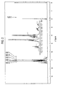
- One exemplary construction of the organic EL device according to the invention is shown in Fig. 1.
- the organic EL device comprises a hole injecting electrode 3, a hole injecting and transporting layer 4, a light emitting layer 5, an electron injecting and transporting layer 6 and an electron injecting electrode 7 in the described order.
- a color filter 8 a fluorescence conversion filter 9
- an organic EL device as mentioned above a sealing layer 10 and a cover 11 are stacked and formed on a glass substrate 2 in the described order, an organic EL color display is then obtained.
- the light emitting layer has functions of injecting holes and electrons, transporting them, and recombining holes and electrons to create excitons.
- the hole injecting and transporting layer has functions of facilitating injection of holes from the hole injecting electrode, providing stable transportation of holes and blocking electrons
- the electron injecting and transporting layer has functions of facilitating injection of electrons from the electron injecting electrode, providing stable transportation of electrons and blocking holes.
- the electron injecting and transporting layer and the hole injecting and transporting layer may be provided, if required, while care is taken of the magnitudes of the functions which the compound used for the light emitting layer has in injecting electrons, transporting electrons, injecting holes, and transporting holes.
- the hole or electron injecting and transporting layer may be dispensed with; that is, the light emitting layer may be allowed to function as a hole injecting and transporting layer or an electron injecting and transporting layer.
- both the hole injecting and transporting layer and the electron injecting and transporting layer may be dispensed with.
- the hole injecting and transporting layer and the electron injecting and transporting layer may be each separated into an injecting layer and a transporting layer.
- the thickness of the organic layer By controlling the thickness of the organic layer while care is taken of the carrier mobility or carrier density (determined depending on ionization potential and electron affinity) of the light emitting layer, electron injecting and transporting layer or hole injecting and transporting layer to be combined therewith, it is possible to freely determine the recombination/light emitting region. It is in turn possible to design the color of light to be emitted, and control emission luminance and spectra due to the interference effect between both electrode as well as the spatial distribution of light emission.
- the carrier mobility or carrier density determined depending on ionization potential and electron affinity
- the compound of the invention may be applied to any one of the hole injecting layer, hole transporting layer, light emitting layer, and hole injecting and transporting layer. Since the compound of the invention is excellent in the capability of injecting holes, however, it is preferably applied to the hole injecting layer or hole injecting and transporting layer, especially the hole injecting layer.
- the compound of the invention that has both the phenylenediamine skeleton and the diamine skeleton including a plurality of phenylene radicals such as a benzidine skeleton, it is possible to freely control ionization potential and carrier mobility without sacrifice of heat resistance and, hence, optimize hole injection efficiency depending on the material to be combined therewith.
- the hole injecting and transporting layer may be formed by the evaporation of the compound of the invention or the coating of a dispersion of the compound of the invention in a resin binder. Especially the evaporation of the compound of the invention yields a good enough amorphous film.
- the fluorescent material used for the light emitting layer may be selected from materials emitting fluorescence of longer wavelength. For instance, a sensible selection may be made from at least one fluorescent material used for the light emitting layer in combination with the compound of the invention. In such a case, too, the compound of the invention may be applied to the light emitting layer.
- the compound of the invention may be used.
- the compound of the invention has the phenylenediamine skeleton contributing to very strong donicity, and so is susceptible to interaction with the light emitting layer, resulting a drop of the intensity of fluorescence due to the formation of exciplexes, etc. This in turn offers problems such as a light emission efficiency drop, and a color purity drop due to the broadening of emission spectra, and so is undesired.
- the compound of the invention may be used as a hole transporting material.
- the hole injecting and transporting layer may be formed of a combination of more than one of hole injecting and transporting materials.
- hole injecting and transporting materials are laminated on ITO in the order of increasing ionization potential, for instance, in the order of a hole injecting layer and a hole transporting layer.
- a hole injecting material having a good thin film property so that a uniform thin film can be formed on the ITO surface having a varying hydrophilic nature. Since evaporation is utilized in the manufacture of devices, films as thin as about 1 to 10 nm can be formed in a uniform and pinhole-free state. If film thickness, refractive index, etc. are regulated, it is then possible to prevent an efficiency drop by controlling the color of light emitted and emission luminance or making use of interference light effects such as the spatial distribution of light emission.
- a triarylamine polymer having a benzidine skeleton alone and less susceptible to interaction with the light emitting material such as those set forth in JP-A's 63-295695, 5-234681 and 7-43564.
- the light emitting layer may contain a fluorescent material.
- the fluorescent material used herein may be at least one compound selected from compounds such as those disclosed in JP-A 63-264692, for instance, quinacridone, rubrene, and styryl dyes.
- Use may also be made of quinoline derivatives such as metal complex dyes containing 8-quinolinol or its derivative as ligands, for instance, tris(8-quinolinolato)aluminum, tetraphenylbutadiene, anthracene, perylene, coronene, and 12-phthaloperinone derivatives.
- Use may further be made of phenyanthracene derivatives disclosed in Japanese Patent Application No. 6-110569, and tetraarylethene derivatives disclosed in Japanese Patent Application 6-114456.
- the fluorescent compound is used in combination with a host substance capable of emitting light by itself; that is, it is preferable that the fluorescent compound is used as a dopant.
- the consent of the fluorescent compound in the light emitting layer is in the range of preferably 0.01 to 10% by weight, and especially 0.1 to 5% by weight.
- Quinolinolato complexes and aluminum complexes containing 8-quinolinol or its derivatives as ligands are preferred for the host substance.
- Such aluminum complexes are typically disclosed in JP-A's 63-264692, 3-255190, 5-70733, 5-258859, 6-215874, etc.
- Exemplary aluminum complexes include tris(8-quinolinolato)aluminum, bis(8-quinolinolato)magnesium, bis(benzo ⁇ f ⁇ -8-quinolinolato)zinc, bis(2-methyl-8-quinolinolato)aluminum oxide, tris(8-quinolinolato)indium, tris(5-methyl-8-quinolinolato)aluminum, 8-quinolinolatolithium, tris(5-chloro-8-quinolinolato)gallium, bis(5-chloro-8-quinolinolato)calcium, 5,7-dichloro-8-quinolinolatoaluminum, tris(5,7-dibromo-8-hydroxyquinolinolato)aluminum, and poly[zinc(II)-bis(8-hydroxy-5-quinolinyl)methane].
- Use may also be made of aluminum complexes containing other ligands in addition to 8-quinolinol or its derivatives, for instance, bis(2-methyl-8-quinolinolato)(phenolato) aluminum (III), bis(2-methyl-8-quinolinolato)(o-cresolato) aluminum (III), bis(2-methyl-8-qinolinolato)(m-cresolato) aluminum (III), bis(2-methyl-8-quinolinolato)(p-cresolato) aluminum (III), bis(2-methyl-8-quinolinolato)(o-phenyl-phenolato)aluminum (III), bis(2-methyl-8-quinolinolato) (m-phenylphenolato)aluminum (III), bis(2-methyl-8-quinolinolato) (p-phenylphenolato)aluminum (III), bis (2-methyl-8-quinolinolato)(2,3-dimethylphenolato)aluminum (III),
- phenylanthracene derivatives disclosed in Japanese Patent Application No. 6-110569 phenylanthracene derivatives disclosed in Japanese Patent Application No. 6-110569, tetraarylethene derivatives disclosed in Japanese Patent Application No. 6-114456, etc.
- the phenylanthracene derivatives are represented by the following formula (VIII): A 1 -L 1 -A 2
- a 1 and A 2 may be identical with or different from each other, and are each a monophenylanthryl or diphenylanthryl group.
- the monophenylanthryl or diphenylanthryl group represented by A 1 , and A 2 may, or may not, have a substituent.
- the substituent for instance, may be an alkyl, aryl, alkoxy, aryloxy or amino group which may have another substituent. Where is substituted by such a substituent is not critical in the invention. However, it is preferable that the phenyl group attached to the anthracene ring rather than the anthracene ring per se is substituted by such a substituent.
- the bond position of the phenyl group in the anthracene ring is the 9- or 10-position in the anthracene ring.
- L 1 stands for a single bond or an arylene group.
- the arylene group given by L 1 is preferably unsubstituted.
- the arylene group includes an ordinary arylene group such as a phenylene group, a biphenylene group, and an anthrylene group as well as two or more such arylene groups attached directly to each other.
- L 1 is preferably a single bond, and a p-phenylene or 4,4'-biphenylene group.
- L 1 may also include two or more such arylene groups as attached to each other via an alkylene group, -O-, -S- or -NR-where R is an alkyl or aryl group.
- R is an alkyl or aryl group.
- a methyl or ethyl group is mentioned for the alkyl group and a phenyl group is mentioned for the aryl group.
- Particular preference is given to the aryl group, for instance, a phenyl group as well as A 1 and A 2 .
- a phenyl group with A 1 or A 2 attached thereto may also be acceptable.
- Preferred for the alkylene group are a methylene group, an ethylene group or the like. Examples of such an arylene group are given below.
- Ar 1 , Ar 2 and Ar 3 may be identical with or different from one another, and are each an aromatic residue.
- Aromatic hydrocarbon groups (aryl groups), and aromatic heterocyclic groups, for instance, may be mentioned for the aromatic residues represented by Ar 1 , Ar 2 and Ar 3 .
- the aromatic hydrocarbon groups may monocyclic or polycyclic aromatic hydrocarbon groups, and include fused rings or ring combinations as well.
- Each aromatic hydrocarbon group has preferably 6 to 30 carbon atoms in all, and may have a substituent represented by an alkyl group, an aryl group, an alkoxy group, an aryloxy group, an amino group or the like.
- aromatic hydrocarbon groups include phenyl, alkylphenyl, alkoxyphenyl, arylphenyl, aryloxyphenyl, aminophenyl, biphenyl, naphthyl, anthryl, pyrenyl, and perylenyl groups.
- the aromatic heterocyclic groups are preferably those containing O, N, and S as a hetero-atom, and may each be a five- or six-membered ring. For instance, thienyl, furyl, pyrrolyl and pyridyl groups are mentioned.
- a phenyl group is particularly preferred for the aromatic group represented by Ar 1 , Ar 2 , and Ar 3 .
- n is an integer of preferably 2 to 6, and especially 2 to 4.
- L 2 is an n-valent aromatic residue. It is preferably a di- to hexa-valent, especially di- to tetra-valent residue derived from an aromatic hydrocarbon, an aromatic heterocyclic ring, an aromatic ether or an aromatic amine. This aromatic residue, which may have a substituent, is preferably unsubstituted.
- the light emitting layer is formed by using the compound of formula (IX) in combination with the aforesaid host material. It is also preferred that the light emitting layer is formed of a mixed layer of at least one compound capable of injecting and transporting holes with at least one compound capable of injecting and transporting electrons. Preferably in this case, a dopant is incorporated in the mixed layer.
- the content of the dopant compound in the mixed layer is in the range of preferably 0.01 to 20% by weight, and especially 0.1 to 15% by weight.
- each carrier migrates in the polarly prevailing substance, so making the injection of carriers having an opposite polarity unlikely to occur. This leads to an increase in the service life of the device due to less damage to the organic compound.
- the compound of formula (IX) in such a mixed layer, it is possible to vary the wavelength performance of light emission that the mixed layer itself possesses, thereby shifting the wavelength of light emission to a longer wavelength side and improving the intensity of light emission, and the stability of the device as well.
- the compound capable of injecting and transporting holes and the compound capable of injecting and transporting electrons, both used to form the mixed layer may be selected from compounds for the injection and transportation of holes and compounds for the injection and transportation of electrons.
- the compounds capable of injecting and transporting electrons it is preferable to use metal complexes containing quinoline derivatives, especially 8-quinolinol or its derivatives as ligands, in particular, tris(8-quinolinolato) aluminum (Alq 3 ). It is also preferable to use the aforesaid phenylanthracene derivatives, and tetraarylamine derivatives.
- amine derivatives having strong fluorescence for instance, hole transporting materials such as tetraphenyldiamine derivatives, styrylamine derivatives, and amine derivatives having an aromatic fused ring, as already mentioned.
- the mixing ratio is determined while the carrier mobility and carrier density are taken into consideration.
- the weight ratio between the compound capable of injecting and transporting holes and the compound capable of injecting and transporting electrons is of the order of 1/99 to 99/1, particularly 10/90 to 90/10, and more particularly 20/80 to 80/20.
- the thickness of the mixed layer must correspond to the thickness of a single molecular layer, and so is preferably less than the thickness of the organic compound layer. More specifically, the mixed layer has a thickness of preferably 1 to 85 nm, especially 5 to 60 nm, and more especially 5 to 50 nm.
- the mixed layer is formed by co-evaporation where the selected compounds are evaporated from different evaporation sources.
- the compounds to be mixed have identical or slightly different vapor pressures (evaporation temperatures), however, they may have previously been mixed together in the same evaporation boat for the subsequent evaporation.
- the compounds are uniformly mixed together in the mixed layer.
- the compounds in an archipelagic form may be present in the mixed layer.
- the light emitting layer may generally be formed at a given thickness by the evaporation of the organic fluorescent substance or coating a dispersion of the organic fluorescent substance in a resin binder.
- the electron injecting and transporting layer may be provided.
- the electron injecting and transporting layer there may be used quinoline derivatives such as organic metal complexes containing 8-quinolinol or its derivatives as ligands, for instance, tris(8-quinolinolato)aluminum (Alq 3 ), oxadiazole derivatives, perylene derivatives, pyridine derivatives, pyrimidine derivatives, quinoxaline derivative, diphenylquinone derivatives, and nitro-substituted fluorene derivatives.
- the electron injecting and transporting layer may also serve as a light emitting layer. In this case, it is preferable to use tris(8-quinolilato)aluminum, etc.
- the electron injecting and transporting layer may then be formed by evaporation or the like.
- the hole, and electron injecting and transporting layer may be formed of various organic compounds as disclosed in JP-A's 63-295695, 2-191694, 3-792 and so on.
- the hole injecting and transporting layer for instance, aromatic tertiary amines, hydrazone derivatives, carbazole derivatives, triazole derivatives, imidazole derivatives, and indole derivatives may be used.
- organic metal complex derivatives such as aluminum quinolinol, oxadiazole derivatives, pyridine derivatives, pyrimidine derivatives, quinoline derivatives, quinoxaline derivative, diphenylquinone derivatives, perylene derivatives and fluorene derivatives may be used.
- the compound of the invention When the compound of the invention is used for the light emitting layer, it is preferable to combine the compound of the invention with the aforesaid light emitting material unlikely to extinguish light due to their interaction.
- the compound of the invention emits strong blue fluorescence, and so can achieve a high-luminance light emitting device when combined with a material having little interaction therewith.
- the thickness of the light emitting layer, the hole injecting and transporting layer, and the electron injecting and transporting layer is not critical and varies with the design of recombination/light emitting region and a particular formation technique although it is usually of the order of preferably 5 to 500 nm, and especially 10 to 200 nm.
- the thickness of the hole injecting and transporting layers, and the electron injecting and transporting layer is equal to, or about 1/10 times to about 10 times as large as, the thickness of the light emitting layer although it depends on the design of the recombination/light emitting region.
- the injecting layer is at least 1 nm thick and the transporting layer is at least 1 nm and especially at least 20 nm thick.
- the upper limit on thickness is usually about 500 nm and especially about 100 nm for the injecting layer and about 500 nm for the transporting layer. The same film thickness applies when two injecting and transporting layers are provided.
- the thickness of the organic layer By controlling the thickness of the organic layer while care is taken of the carrier mobility or carrier density (determined depending on ionization potential and electron affinity) of the light emitting layer, electron injecting and transporting layer or hole injecting and transporting layer to be combined therewith, it is possible to freely determine the recombination/light emitting region. It is in turn possible to design the color of light to be emitted, and control emission luminance and spectra due to the interference effect between both electrode as well as the spatial distribution of light emission.
- the carrier mobility or carrier density determined depending on ionization potential and electron affinity
- the electron injecting electrode it is preferable to use a material having a low work function, for instance, Li, Na, K, Mg, Al, Ag or In, an alloy thereof, or an oxide or halide thereof. It is also preferred that the electron injecting electrode be formed of fine crystal grains, especially in an amorphous state.
- the electron injecting electrode has preferably a thickness of the order of 10 to 1,000 nm.
- the hole injecting electrode is preferably transparent or semitransparent. Since there is some limitation on the material of which the electron injecting electrode is formed as mentioned above, however, the material and thickness of the hole injecting electrode are preferably determined such that at least 80% of the light emitted transmits through it. For instance, it is preferable to use ITO (tin-doped indium oxide), IZO (zinc-doped indium oxide), SnO 2 , Ni, Au, Pt, Pd, and polypyrrole for the hole injecting electrode. It is also preferable that the hole injecting electrode has a thickness of the order of 10 to 500 nm.
- the driving voltage be low.
- an ITO of 10 to 30 ⁇ / ⁇ (with a thickness of 80 to 300 nm).
- the thickness and optical constant of the ITO may be designed such that high light extraction efficiency and high color purity are satisfied by the interference effect due to reflection at the ITO interface.
- an Al interconnection may be applied because the resistance of the ITO increases.
- transparent or translucent materials such as glasses, and resins are used for the substrate material because, in the illustrated embodiment, the emitted light is extracted or taken out of the substrate side.
- the substrate may be colored or otherwise provided with a color filter film, fluorescence conversion film or dielectric reflecting film for controlling the color of light emitted.
- a color filter employed with liquid crystal display devices may be used.
- an optical thin film such as a dielectric multilayer film may be used.
- the fluorescence conversion film absorbs light emitted from an EL device and gives out light from the phosphors contained therein for the color conversion of light emission, and is composed of three components, a binder, a fluorescent material and a light absorbing material.
- a fluorescent material having high fluorescent quantum efficiency and especially a fluorescent material having strong absorption in an EL light emission wavelength region.
- Laser dyes are suitable for the practice of the invention.
- rohodamine compounds perylene compounds, cyanine compounds, phthalocyanine compounds (including subphthalocyanine compounds, etc.), naphthaloimide compounds, fused cyclic hydrocarbon compounds, fused heterocyclic compounds, styryl compounds, and coumarin compounds.
- the binder it is basically preferable to make an appropriate selection from materials that do not extinguish fluorescence. It is particularly preferable to use a material that can be finely patterned by photolithography, printing or the like. It is also preferable to use a material that is not damaged during ITO film formation.
- the light absorbing material is used when light is not fully absorbed by the fluorescent material, and so may be dispensed with, if not required.
- the light absorbing material it is preferable to make a selection from materials that do not extinguish the fluorescence of the fluorescent material.
- vapor phase growth processes such as evaporation, and sputtering.
- the hole injecting and transporting layer, the light emitting layer, and the electron injecting and transporting layer it is preferable to use a vacuum evaporation technique which enables a homogeneous thin film to be obtained.
- a vacuum evaporation technique which enables a homogeneous thin film to be obtained.
- the vacuum evaporation process it is possible to obtain homogeneous thin films in an amorphous state or with a crystal grain diameter of at most 0.1 ⁇ m.
- the use of a thin film having a crystal grain diameter exceeding 0.1 ⁇ m results in non-uniform light emission. To avoid this, it is required to increase the driving voltage of the device; however, there is a striking drop of hole injection efficiency.
- an evaporation rate of the order of 0.01 to 1 nm/sec. is preferably applied at a degree of vacuum of up to 10 -5 Torr (10 -4 Pa). It is also preferable to form the layers continuously in vacuum. If the layers are continuously formed in vacuum, high properties are then obtained because the adsorption of impurities on the interface between the adjacent layers can be avoided. In addition, the driving voltage of the device can be lowered while the growth and occurrence of dark spots are inhibited.
- the EL device of the invention is generally of the DC drive type while it may be of the AC or pulse drive type.
- the applied voltage is generally of the order of 2 to 20 volts.
- HIM34 N,N'-diphenyl-N,N'-bis[N-phenyl-N-4-tolyl(4-aminophenyl)]benzidine referred to below as HIM34 was obtained as in synthesis example 1 with the exception that 4-iodotoluene was used in place of 3-iodotoluene.
- HIM38 N,N'-diphenyl-N,N'-bis[N-phenyl-N-4-tolyl(4-aminophenyl)]benzidine referred to below as HIM38 was obtained as in synthesis example 1 with the exception that 4-iodonaphthalene was used in place of 3-iodotoluene.
- HIM35 N,N'-diphenyl-N,N'-bis[N-phenyl-N-4-tolyl(4-aminophenyl)]benzidine referred to below as HIM35 was obtained as in synthesis example 1 with the exception that 3-iodobiphenyl was used in place of 3-iodotoluene.
- N,N'-diphenyl-N-(3-tolyl)-1,4-phenylenediamine was obtained.
- reaction vessel 17.5 grams of N,N'-diphenyl-N-3-tolylphenylenediamine and 32 grams of 1,4-diiodobenzene were heated together with 0.3 grams of activated copper powders, 50 grams of potassium carbonate and 50 ml of decalin at an oil bath temperature of 200°C for 24 hours in an Ar atmosphere. After the completion of the reaction, the reaction solution was filtrated with the addition of 100 ml of toluene thereto, thereby removing insolubles. The filtrate was washed with water, and dried over sodium sulfate. Following this, the solvent was removed by distillation from the filtrate.
- HIM74 N,N'-diphenyl-N,N'-bis[N-phenyl-N-[N-phenyl-N-4-tolyl(4-aminophenyl)](4-aminophenyl)]benzidine referred to below as HIM74 was obtained as in synthesis example 5 with the exception that 4-iodotoluene was used instead of 3-iodotoluene.
- HIM 78 N,N'-diphenyl-N,N'-bis ⁇ N-phenyl-N-[N-phenyl-N-1-naphthyl (4-aminophenyl)](4-aminophenyl) ⁇ benzidine referred to below as HIM 78 was obtained as in synthesis example 5 with the exception that 1-iodonaphthalene was used instead of 3-iodotoluene.
- reaction vessel 21 grams of N,N'-diphenyl-N-3-tolylphenylenediamine and 10 grams of 4,4''-diiodo-p-terphenyl were heated together with 0.3 grams of activated copper powders, 50 grams of potassium carbonate and 50 ml of decalin at an oil bath temperature of 200°C for 24 hours in an Ar atmosphere. After the completion of the reaction, the reaction solution was filtrated with the addition of 100 ml of toluene thereto for removal of insolubles, and the filtrate was washed with water and dried over sodium sulfate.
- a glass substrate having a 100 nm-thick ITO transparent electrode (a hole injecting electrode) was ultrasonically washed with neutral detergent, acetone, and ethanol, and then pulled up from boiling ethanol, followed by drying.
- This substrate was cleaned with UV/O 3 , and fixed to a substrate holder in a vacuum evaporation system, which was evacuated to a vacuum of 1 x 10 -6 Torr (10 -4 Pa).
- tris(quinolinolato)aluminum Alq 3
- Alq 3 tris(quinolinolato)aluminum
- MgAg (having a weight ratio of 10:1) was evaporated at a deposition rate of 0.2 nm/sec. to a thickness of 200 nm to form an electron injecting electrode. Finally, Al was evaporated to a thickness of 100 nm to form a protective layer, thereby obtaining an organic EL device.
- the half life of luminance was 500 hours (with an initial luminance of 2,030 cd/m 2 , an initial driving voltage of 6.55 V, and a driving voltage increase of 3.5 V).
- HIM34 compound No. 2
- HIM33 compound No. 3
- the half life of luminance was 800 hours (with an initial luminance of 2,040 cd/m 2 , an initial driving voltage of 6.59 V, and a driving voltage increase of 3.0 V).
- HIM38 compound No. 16
- HIM33 compound No. 3
- the half life of luminance was 1,600 hours (with an initial luminance of 1,923 cd/m 2 , an initial driving voltage of 6.59 V, and a driving voltage increase of 1.5 V).
- HIM73 compound No. 26
- HIM 33 compound No. 3
- the half life of luminance was 1,000 hours (with an initial luminance of 1,841 cd/m 2 , an initial driving voltage of 6.76 V, and a driving voltage increase of 2.5 V).
- HIM74 compound No. 25
- HIM33 compound No. 3
- the half life of luminance was 1,000 hours (with an initial luminance of 1,841 cd/m 2 , an initial driving voltage of 6.76 V, and a driving voltage increase of 1.5 V).
- a device was prepared as in example 1 with the exception that N,N'-diphenyl-N,N'-bis[N-phenyl-N-4-tolyl(4-aminophenyl)]benzidine (HIM35: compound No. 10) or N,N'-diphenyl-N,N'-bis ⁇ N-phenyl-N-[N-phenyl-N-1-naphthyl(4-aminophenyl)](4-aminophenyl) ⁇ benzidine (HIM78: compound No. 40) was used in place of the aforesaid HIM33 (compound No. 3). Equivalent results as in example 1 were obtained. Even with other exemplified compounds, equivalent results were obtained.
- a device was prepared as in example 1. Instead of the hole transporting layer of example 1, however, a hole transporting and light emitting layer was formed by mixing a hole transporting material TPD, rubrene, i.e., a light emitting material having such a structure as given below and aluminum quinolinol (Alq 3 ), i.e., an electron injecting material having such a structure as given below at a weight mixing ratio of 5:5:1 to form a mixed layer of 40 nm in thickness by means of triple co-evaporation. Thereafter, aluminum quinolinol (Alq 3 ) was evaporated to a thickness of 30 nm.
- TPD hole transporting material
- rubrene i.e., a light emitting material having such a structure as given below
- Al quinolinol (Alq 3 ) aluminum quinolinol
- the half life of luminance was 30,000 hours (2,350 cd/m 2 and a driving voltage increase of 1.0 V), and the half life was 10,000 hours or longer when the initial luminance was 300 cd/m 2 .
- the hole transporting layer of example 1 was formed of TPD alone, the thickness of the Alq 3 light emitting layer was changed to 10 nm, and a tetraphenylethene or phenylanthracene layer of 30 nm in thickness was interleaved between the hole transporting layer and the light emitting layer. Consequently, equivalent results as mentioned above were obtained.
- a device was prepared as in example 1 with the exception that 4,4',4''-tris[-N-(-3-methylphenyl)-N-phenylamino] triphenylamine (MTDATA) having such a structure as given below was used in place of HIM33 (compound No. 3).
- MTDATA 4,4',4''-tris[-N-(-3-methylphenyl)-N-phenylamino] triphenylamine
- a device was prepared as in example 1 with the exception that copper phthalocyanine having such a structure as given below and a thickness of 10 nm was used for HIM33 (compound No. 3).
- a glass substrate having a 100 nm-thick ITO transparent electrode (a hole injecting electrode) was ultrasonically washed with neutral detergent, acetone, and ethanol, and then pulled up from boiling ethanol, followed by drying.
- This substrate was cleaned with UV/O 3 , and fixed to a substrate holder in a vacuum evaporation system, which was evacuated to a vacuum of 1 x 10 -6 Torr (10 -4 Pa).
- Al was evaporated at a deposition rate of 2 nm/sec. to a thickness of 200 nm to form an electron injecting electrode, thereby obtaining a single layer device.
- the Hole mobility was found to be 2.7 x 10 -3 cm 2 /Vs as measured by the time-of-flight method. This value is at least twice as high as that of a general hole injecting and transporting material TPD, i.e., N,N'-bis(3-methylphenyl)-N,N'-diphenyl-1,1'-biphenyl-4,4'-diamine.
- a device was obtained as in example 9 with the exception that the aforesaid MTDATA was used in place of HIM34.
- the device of the invention makes it possible to obtain a much higher current density at the same voltage because of its enhanced hole supply efficiency.
- An organic EL device was prepared as in example 2 with the exception that the thickness of the hole injecting layer containing N,N'-diphenyl-N,N'-bis[N-phenyl-N-4-tolyl(4-aminophenyl)]benzidine (HIM34: compound No. 2) was changed from 50 nm to 300 nm.
- the half life of luminance was 1,500 hours (with an initial luminance of 1,800 cd/m 2 , an initial driving voltage of 7.6 V, and a driving voltage increase of 3.0 V).
- the organic EL device constructed using the compound of the invention is substantially free from a driving voltage increase or a luminance drop and a current leakage with neither development nor growth of local non-emitting spots while it is driven, and so is capable of emitting light with high luminance, and high reliability such as high heat resistance.
- the optimum work function can be imparted to a hole injecting electrode or an organic material combined therewith, so that a device emitting light continuously with high reliability can be achieved.
Landscapes
- Chemical & Material Sciences (AREA)
- Engineering & Computer Science (AREA)
- Materials Engineering (AREA)
- Physics & Mathematics (AREA)
- Spectroscopy & Molecular Physics (AREA)
- Organic Chemistry (AREA)
- Optics & Photonics (AREA)
- Electroluminescent Light Sources (AREA)
- Organic Low-Molecular-Weight Compounds And Preparation Thereof (AREA)
Abstract


Description
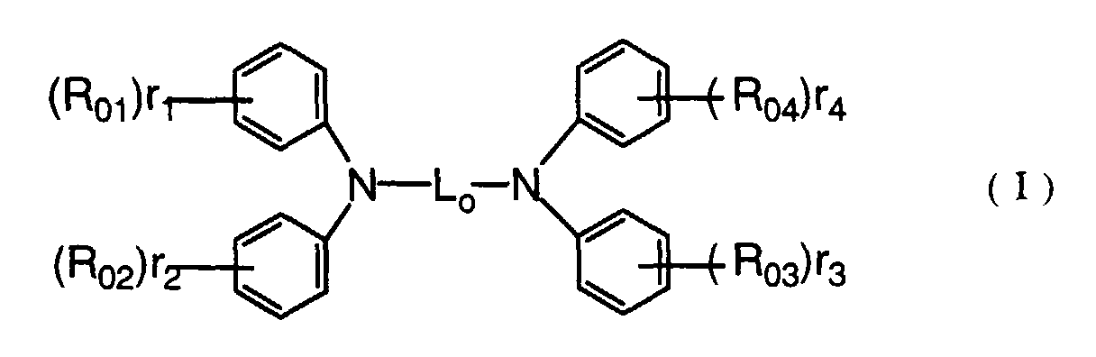


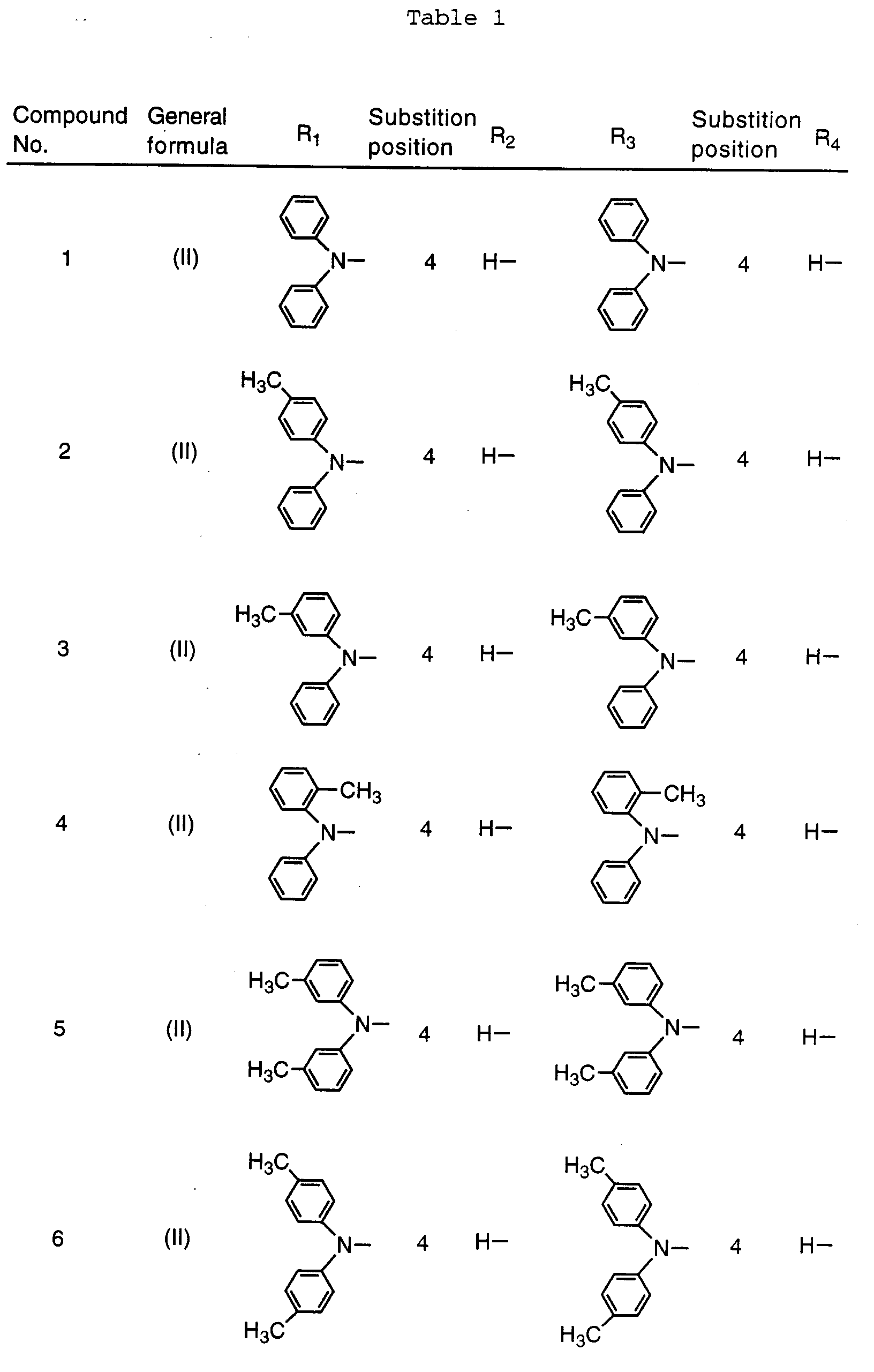


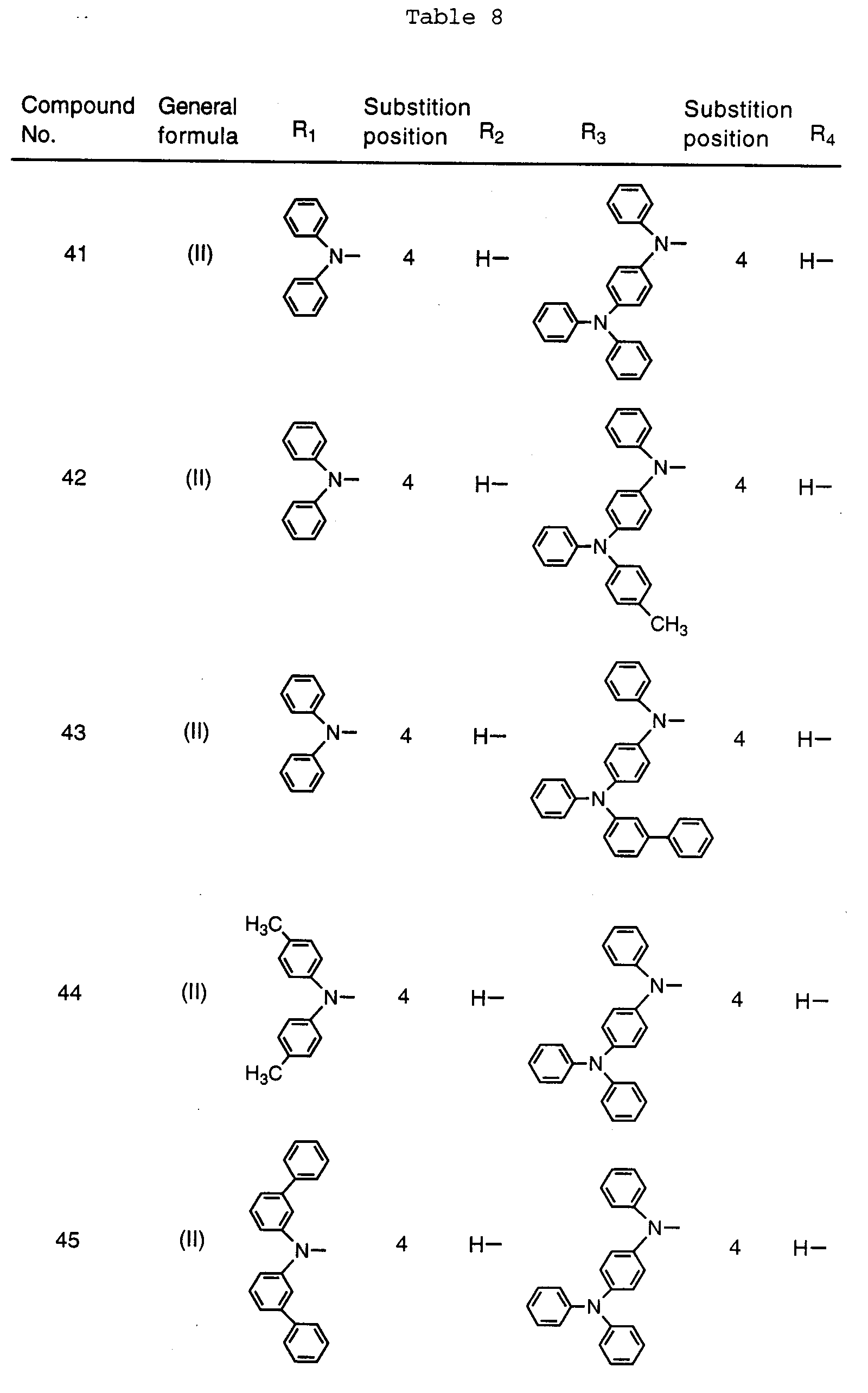


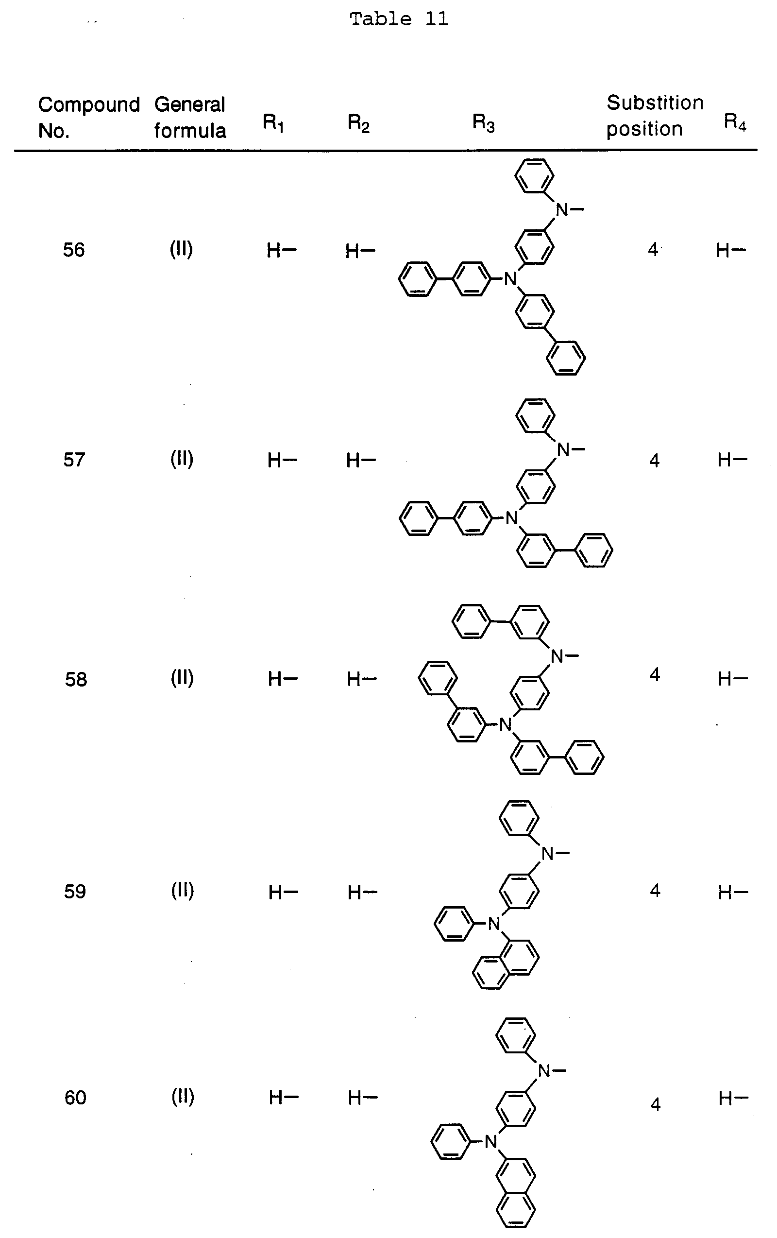


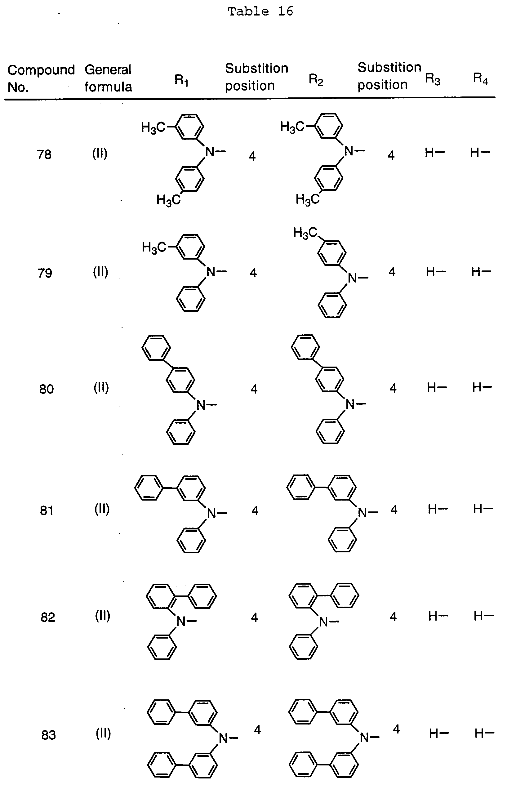


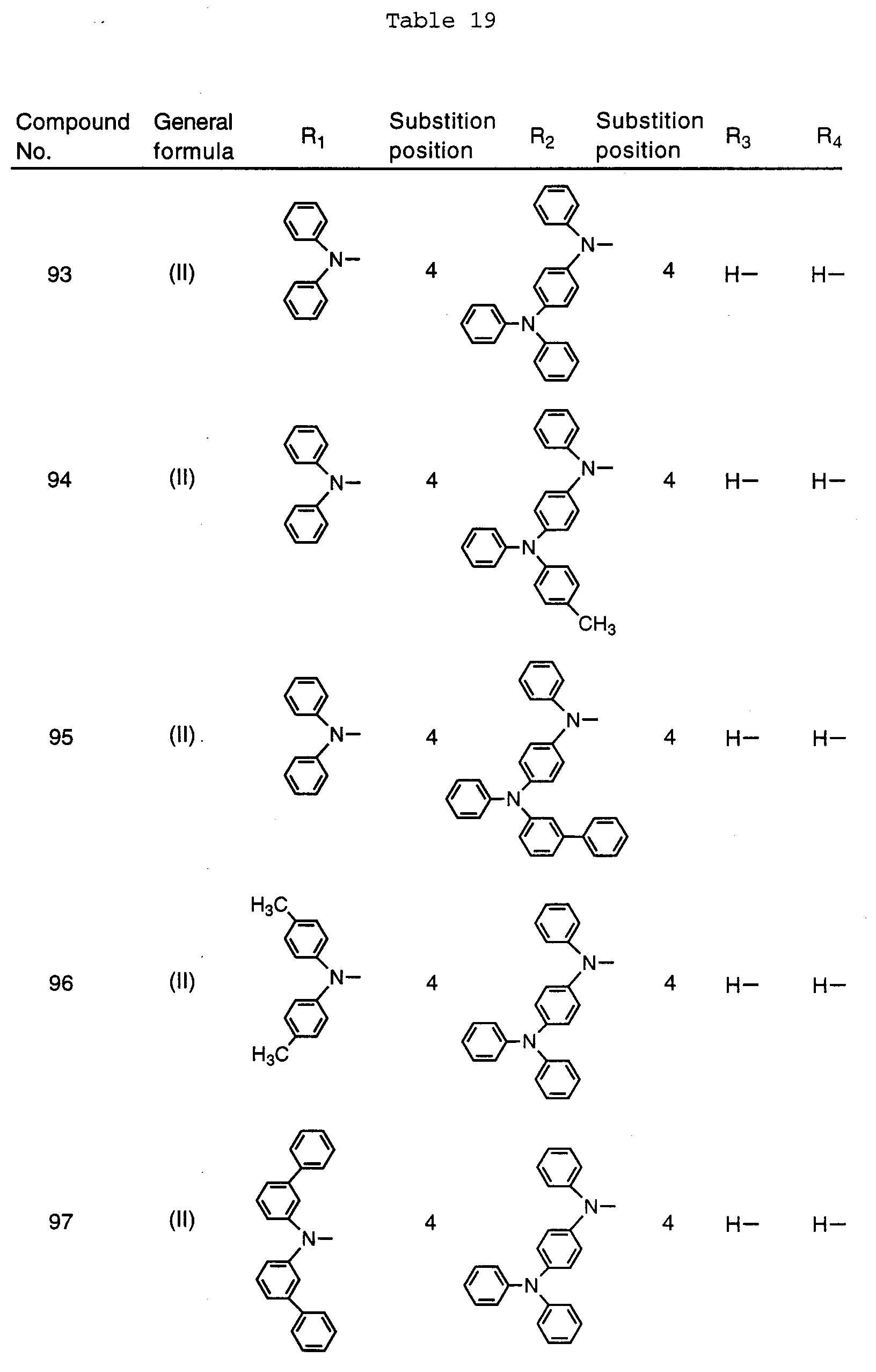

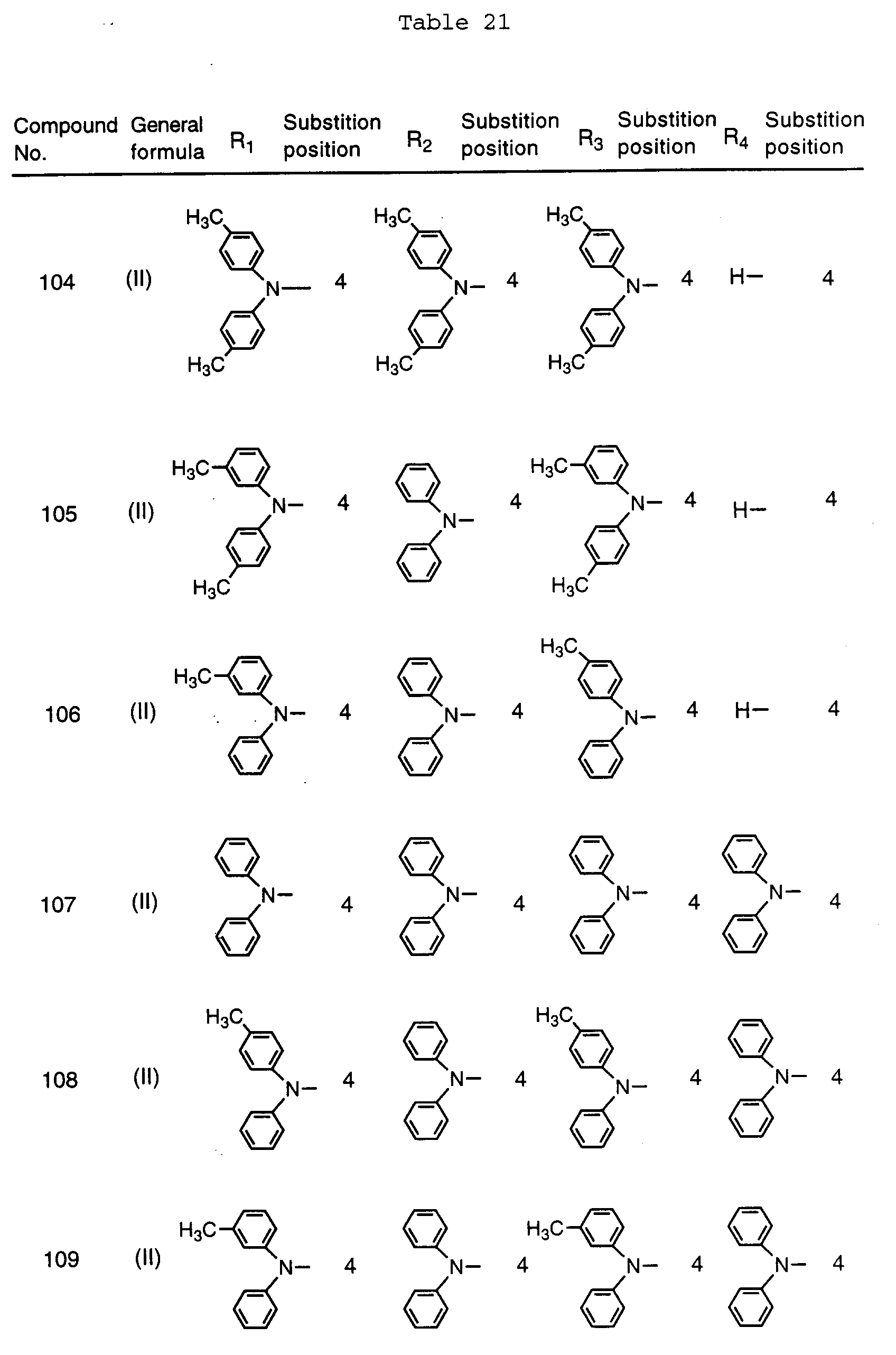
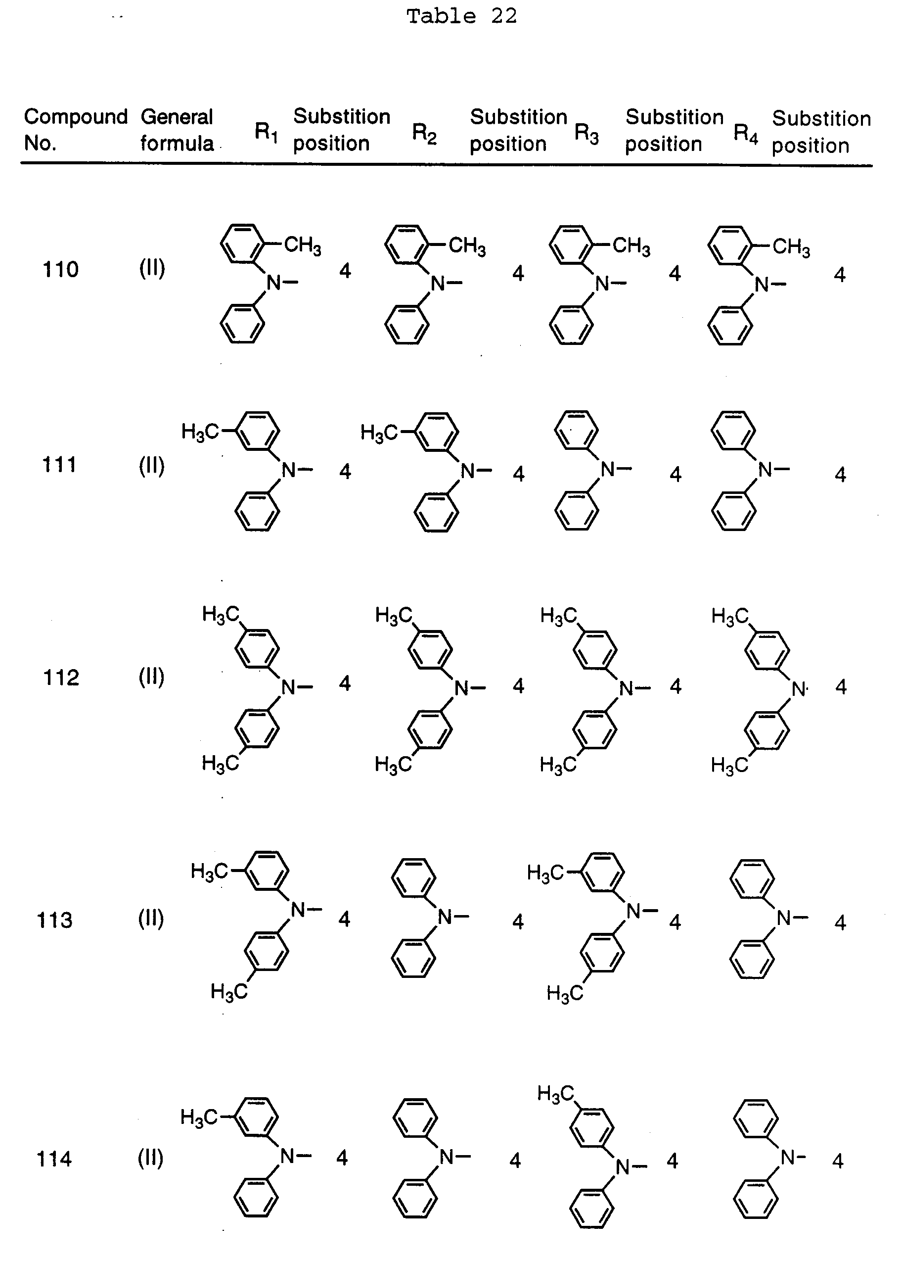


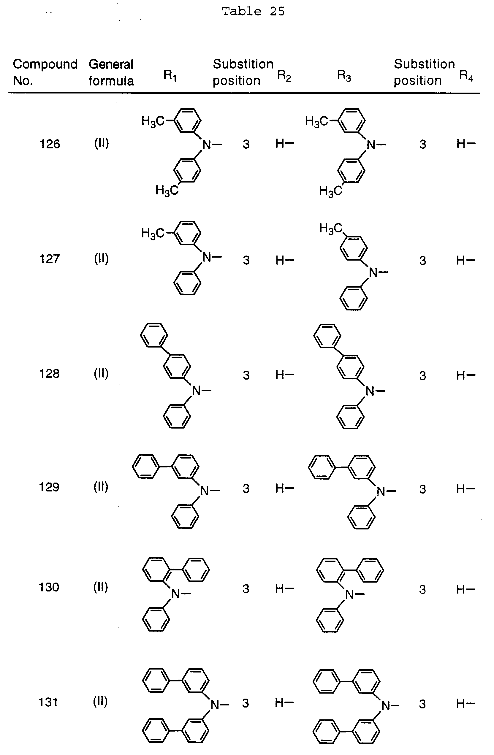


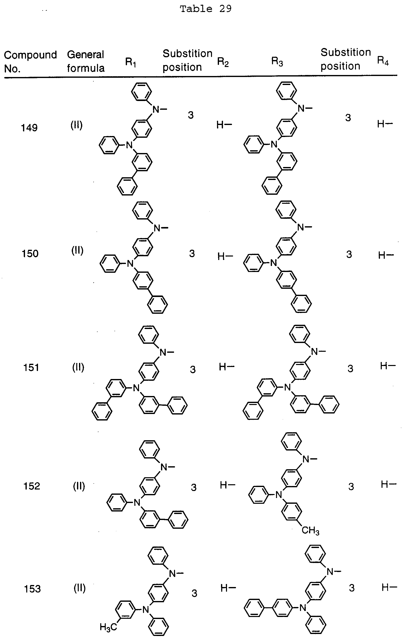


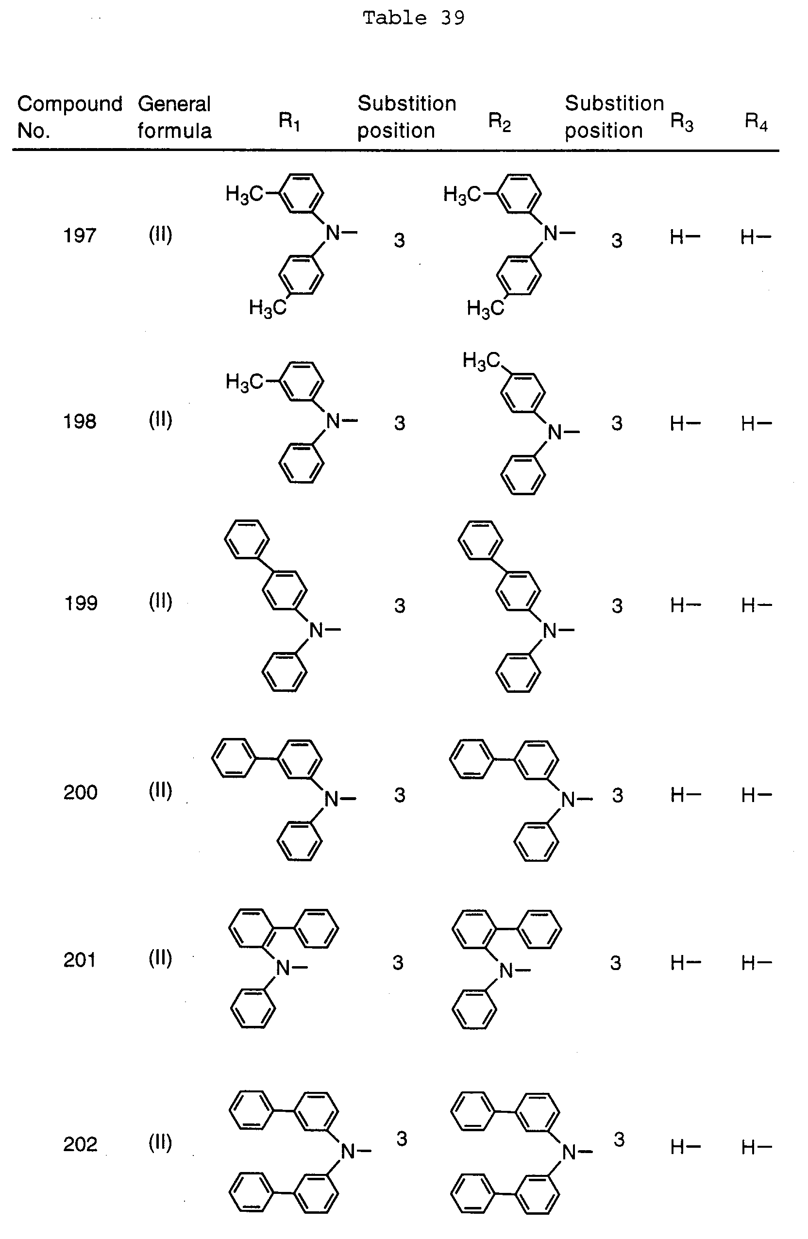


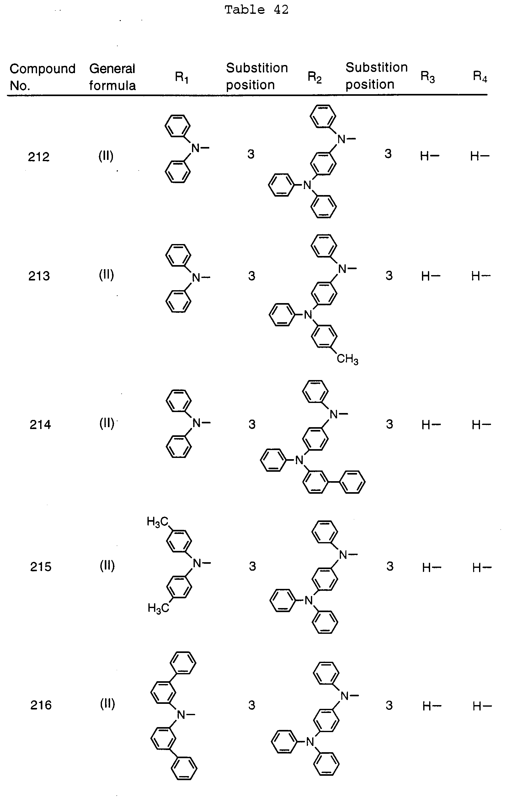


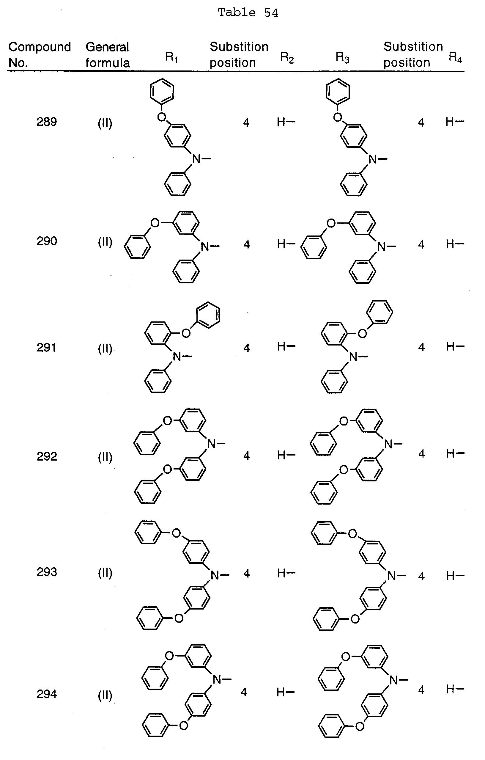
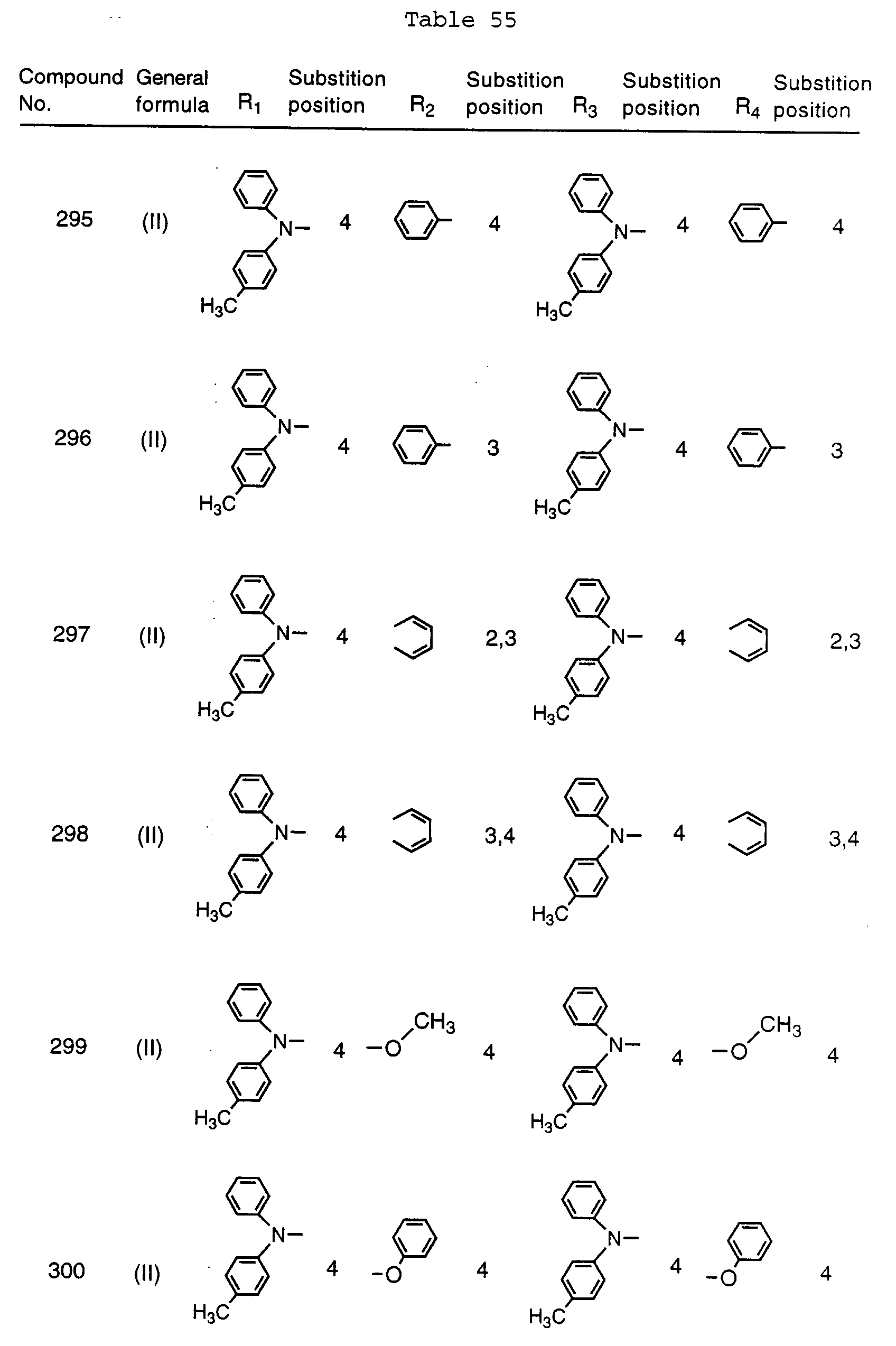


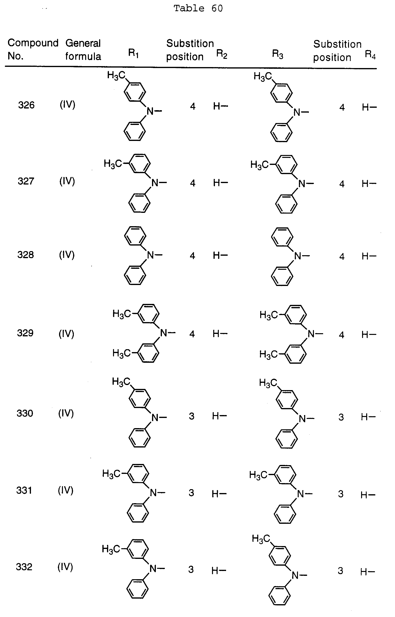

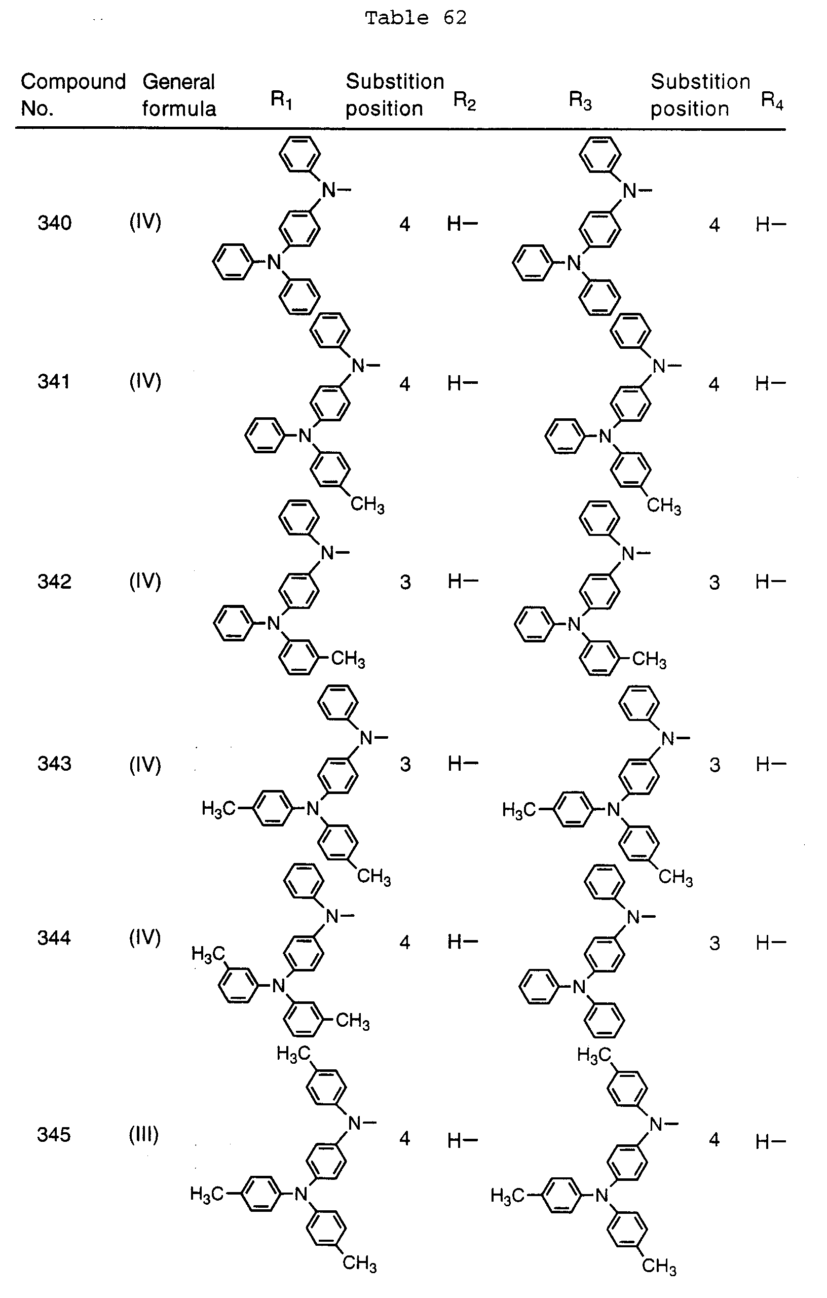
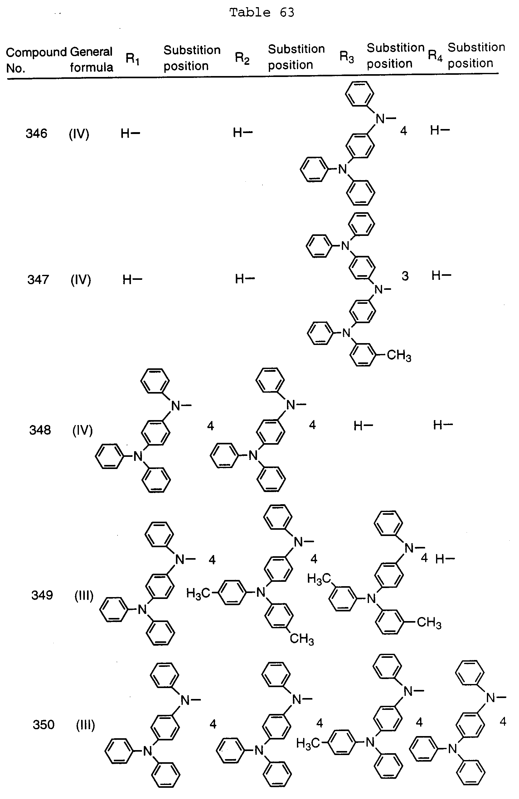


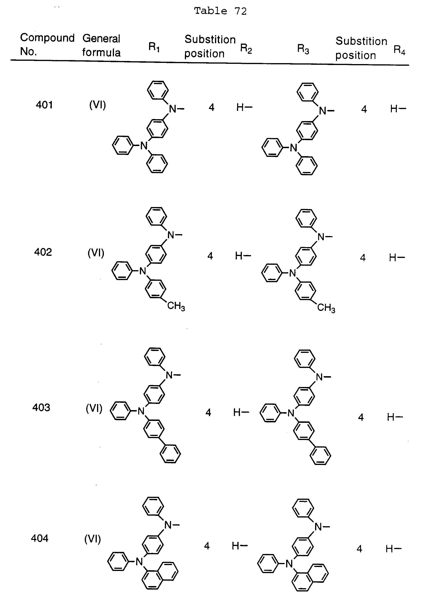


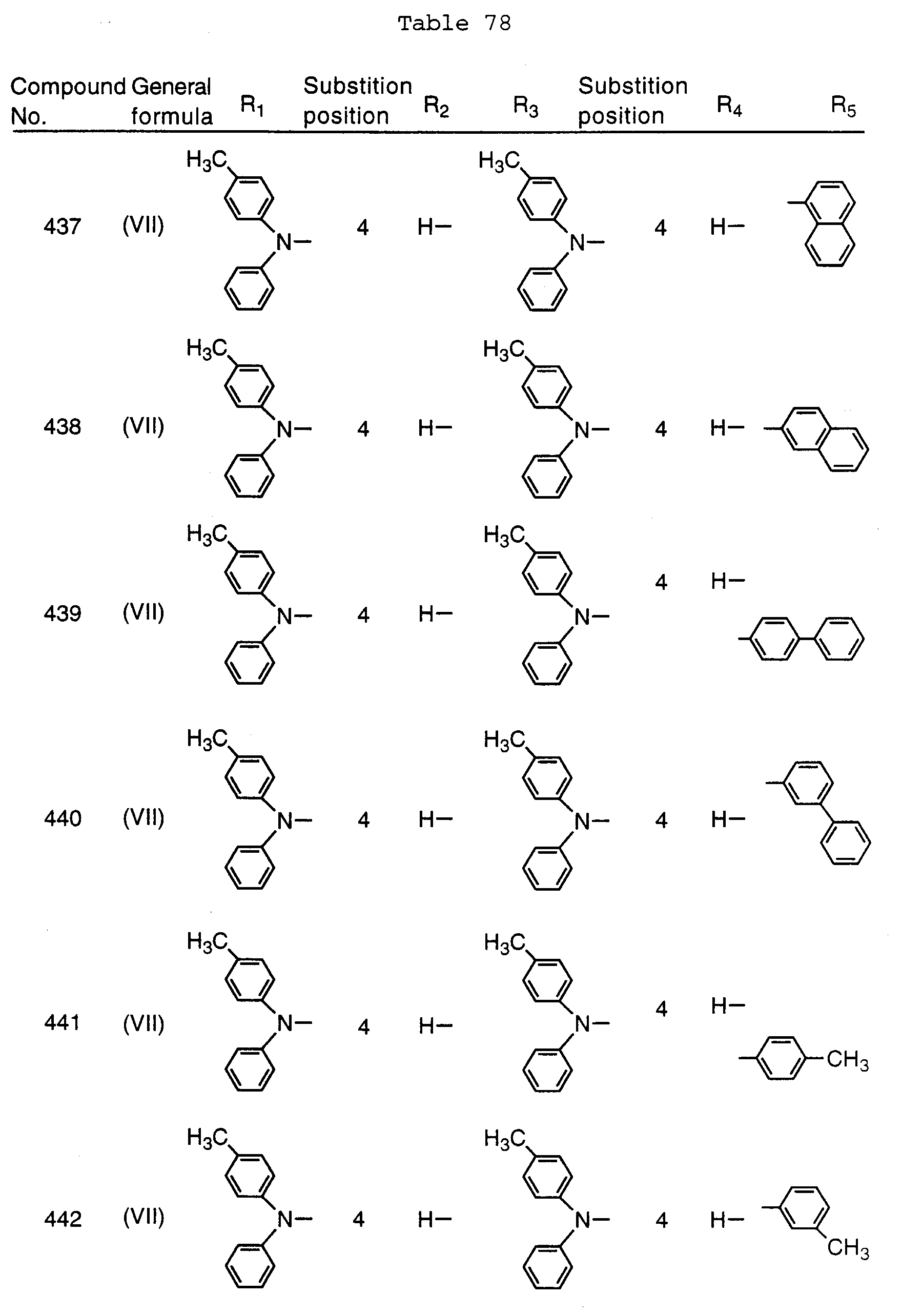
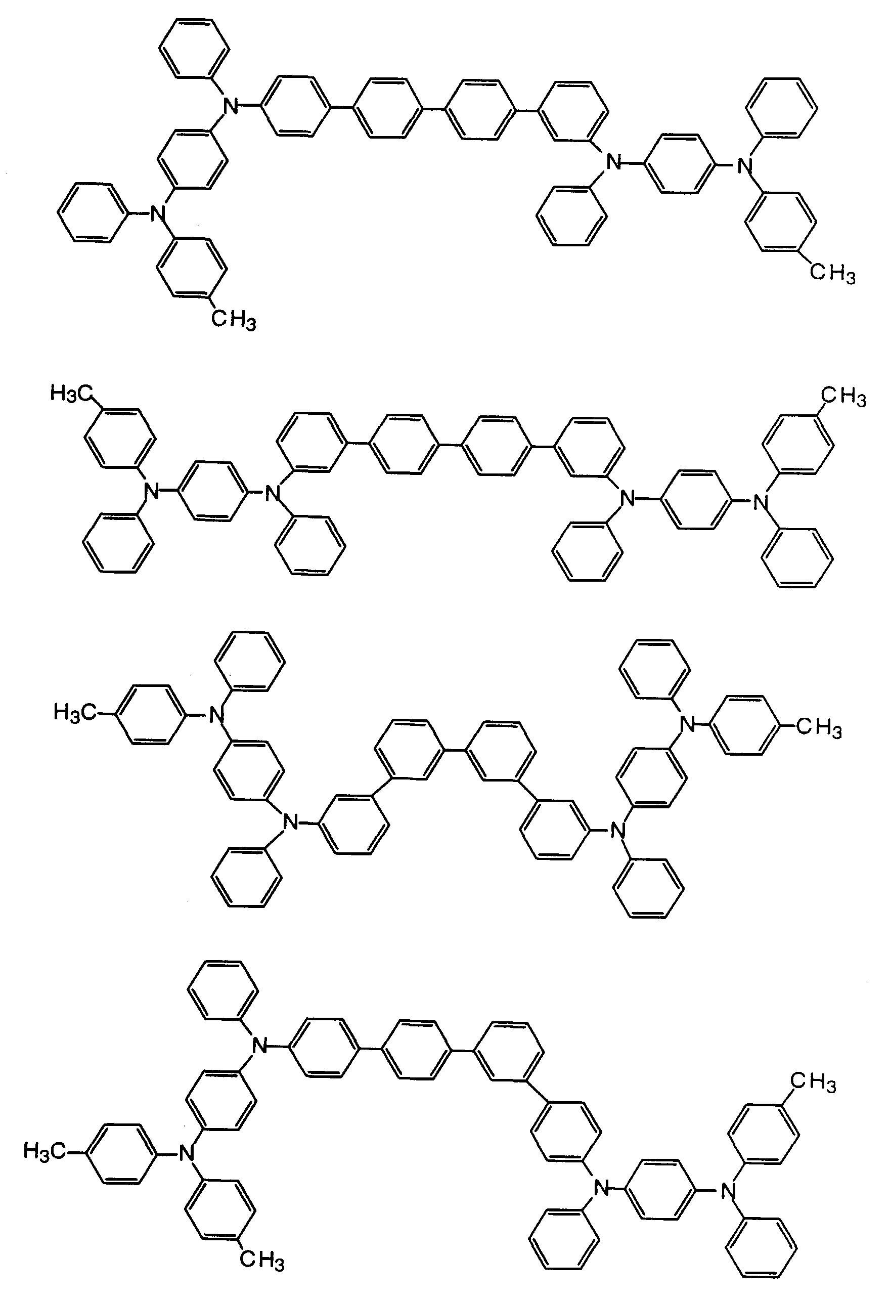


Claims (11)
- An organic EL device comprising organic compound layers, at least one of which has a skeleton represented by formula (I):where L0 is any one of o-, p-, and m-phenylene groups which have two, three or four rings and which may have a substituent with the proviso that when L0 is a phenylene group having four rings, the phenylene group may have an unsubstituted or substituted aminophenyl group somewhere therein, R01, R02, R03 and R04 are each any one of the following groups:
 where R11, R12, R13, R14, R15, R16 and R17 are each a substituted or unsubstituted aryl group, and r1, r2, r3 and r4 are each an integer of 0 to 5 with the proviso that
- The organic EL device of claim 1, wherein a set of phenylene groups represented by L0 is a 4,4'-biphenylene group.
- An organic EL device comprising at least two organic compound layers, wherein the organic compound layer recited in claim 1 or 2 is an organic compound layer having a function of injecting and transporting holes.
- An organic EL device comprising three or more layers including at least an organic compound layer having a function of injecting holes and at least an organic compound layer having a function of transporting holes, wherein:the organic compound layer recited in claim 1 or 2 is an organic compound layer having said function of injecting holes.
- The organic EL device of claim 3 or 4, wherein at least one layer of said organic compound layers includes a light emitting layer containing a hole transporting compound and an electron transporting compound.
- The organic EL device of claim 5, wherein said light emitting layer exists between the organic compound layer having a function of injecting holes and/or the organic compound layer having a function of transporting holes and the organic compound layer having a function of transporting electrons and/or an organic compound layer having a function of injecting electrons.
- An organic EL device comprising a hole injecting electrode, and including at least an organic compound layer having a function of injecting and transporting holes as recited in claim 3, an organic compound layer having a function of transporting holes, a light emitting layer, and an electron injecting electrode laminated on said hole injecting electrode in the described order.
- An organic EL device comprising a hole injecting electrode, and including at least an organic compound layer having a function of injecting holes as recited in claim 4, a light emitting layer, and an electron injecting electrode laminated on said hole injecting electrode in the described order.
- The organic EL device of any one of claims 3 to 8, wherein said organic compound layer having a function of injecting holes has a thickness of at least 100 nm.
- The organic EL device of any one of claims 5 to 9, wherein said layer containing said compound has a Hole mobility of at least 1.0 x 10⁻³ cm2/Vs.
- The organic EL device of any one of claim 5 to 10, wherein the Hole mobility of said layer containing said compound is up to a half of that of said light emitting layer.
Applications Claiming Priority (3)
| Application Number | Priority Date | Filing Date | Title |
|---|---|---|---|
| JP35841696 | 1996-12-28 | ||
| JP358416/96 | 1996-12-28 | ||
| PCT/JP1997/004904 WO1998030071A1 (en) | 1996-12-28 | 1997-12-26 | Organic electroluminescent elements |
Publications (4)
| Publication Number | Publication Date |
|---|---|
| EP0891121A1 true EP0891121A1 (en) | 1999-01-13 |
| EP0891121A4 EP0891121A4 (en) | 2003-01-02 |
| EP0891121B1 EP0891121B1 (en) | 2012-09-26 |
| EP0891121B8 EP0891121B8 (en) | 2013-01-02 |
Family
ID=18459187
Family Applications (1)
| Application Number | Title | Priority Date | Filing Date |
|---|---|---|---|
| EP97950436A Expired - Lifetime EP0891121B8 (en) | 1996-12-28 | 1997-12-26 | Organic electroluminescent elements |
Country Status (4)
| Country | Link |
|---|---|
| US (3) | US6344283B1 (en) |
| EP (1) | EP0891121B8 (en) |
| JP (3) | JP3654909B2 (en) |
| WO (1) | WO1998030071A1 (en) |
Cited By (169)
| Publication number | Priority date | Publication date | Assignee | Title |
|---|---|---|---|---|
| EP1029909A1 (en) * | 1998-09-09 | 2000-08-23 | Idemitsu Kosan Co., Ltd. | Organic electroluminescence device and phenylenediamine derivative |
| EP1030382A2 (en) * | 1999-02-18 | 2000-08-23 | Pioneer Corporation | Organic electroluminescence device and process for fabricating the same |
| WO2001023344A1 (en) * | 1999-09-30 | 2001-04-05 | Idemitsu Kosan Co., Ltd. | Amine compound and organic electroluminescence element using the same |
| WO2002094965A1 (en) * | 2001-05-24 | 2002-11-28 | Idemitsu Kosan Co., Ltd. | Organic electroluminescence element |
| EP1311009A2 (en) * | 2001-11-08 | 2003-05-14 | Xerox Corporation | Organic light emitting devices |
| US6610455B1 (en) | 2002-01-30 | 2003-08-26 | Eastman Kodak Company | Making electroluminscent display devices |
| WO2003074628A1 (en) * | 2002-03-04 | 2003-09-12 | Cdt Oxford Limited | Phosphorescent compositions and organic light emitting devices containing them |
| EP1367677A2 (en) | 2002-05-28 | 2003-12-03 | Eastman Kodak Company | Lighting apparatus with flexible oled area illumination light source and fixture |
| EP1443093A1 (en) * | 2003-01-29 | 2004-08-04 | Samsung SDI Co., Ltd. | Molecular chemical compounds capable of emitting photoluminescence comprising electron shiftable structures and their use in photoluminescence erasure display devices |
| WO2004099338A2 (en) * | 2002-09-25 | 2004-11-18 | 3M Innovative Properties Company | Organic electroluminescent compositions |
| US6849345B2 (en) | 2001-09-28 | 2005-02-01 | Eastman Kodak Company | Organic electroluminescent devices with high luminance |
| US6872472B2 (en) | 2002-02-15 | 2005-03-29 | Eastman Kodak Company | Providing an organic electroluminescent device having stacked electroluminescent units |
| US6890627B2 (en) | 2002-08-02 | 2005-05-10 | Eastman Kodak Company | Laser thermal transfer from a donor element containing a hole-transporting layer |
| US6919140B2 (en) | 2003-07-10 | 2005-07-19 | Eastman Kodak Company | Organic electroluminescent devices with high luminance |
| US6939660B2 (en) | 2002-08-02 | 2005-09-06 | Eastman Kodak Company | Laser thermal transfer donor including a separate dopant layer |
| WO2006034028A2 (en) | 2004-09-21 | 2006-03-30 | Eastman Kodak Company | Delivering particulate material to a vaporization source |
| EP1666561A1 (en) * | 1998-12-28 | 2006-06-07 | Idemitsu Kosan Company Limited | Organic electroluminescent element |
| US7094902B2 (en) | 2002-09-25 | 2006-08-22 | 3M Innovative Properties Company | Electroactive polymers |
| US7192657B2 (en) | 2003-04-15 | 2007-03-20 | 3M Innovative Properties Company | Ethynyl containing electron transport dyes and compositions |
| US7221332B2 (en) | 2003-12-19 | 2007-05-22 | Eastman Kodak Company | 3D stereo OLED display |
| US7241512B2 (en) | 2002-04-19 | 2007-07-10 | 3M Innovative Properties Company | Electroluminescent materials and methods of manufacture and use |
| US7271406B2 (en) | 2003-04-15 | 2007-09-18 | 3M Innovative Properties Company | Electron transport agents for organic electronic devices |
| US7282275B2 (en) | 2002-04-19 | 2007-10-16 | 3M Innovative Properties Company | Materials for organic electronic devices |
| US7402343B2 (en) | 2003-01-29 | 2008-07-22 | Samsung Sdi Co., Ltd. | Molecular chemical compounds with structures allowing electron displacement and capable of emitting photoluminescent radiation, and photoluminescence quenching device employing the same |
| EP2161272A1 (en) | 2008-09-05 | 2010-03-10 | Basf Se | Phenanthrolines |
| US7732811B2 (en) | 2006-12-04 | 2010-06-08 | Semiconductor Energy Laboratory Co., Ltd. | Light-emitting element, light-emitting device, and electronic device |
| WO2010083869A2 (en) | 2009-01-23 | 2010-07-29 | Merck Patent Gmbh | Materials for organic electroluminescence devices |
| WO2010094378A1 (en) | 2009-02-17 | 2010-08-26 | Merck Patent Gmbh | Organic electronic device |
| US7799439B2 (en) | 2006-01-25 | 2010-09-21 | Global Oled Technology Llc | Fluorocarbon electrode modification layer |
| WO2010108579A1 (en) | 2009-03-23 | 2010-09-30 | Merck Patent Gmbh | Organic electroluminescent device |
| WO2010114749A1 (en) | 2009-04-03 | 2010-10-07 | Global Oled Technology Llc | Tandem white oled with efficient electron transfer |
| EP2239352A2 (en) | 2004-09-21 | 2010-10-13 | Global OLED Technology LLC | Delivering particulate material to a vaporization zone |
| WO2010115498A1 (en) | 2009-04-09 | 2010-10-14 | Merck Patent Gmbh | Organic electroluminescence device |
| WO2010149259A2 (en) | 2009-06-22 | 2010-12-29 | Merck Patent Gmbh | Conducting formulation |
| EP2276089A2 (en) | 2004-07-27 | 2011-01-19 | Global OLED Technology LLC | Method for reducing moisture contamination in a top-emitting oled using a dessicant |
| WO2011015265A2 (en) | 2009-08-04 | 2011-02-10 | Merck Patent Gmbh | Electronic devices comprising multi cyclic hydrocarbons |
| US7893427B2 (en) | 2004-07-23 | 2011-02-22 | Semiconductor Energy Laboratory Co., Ltd. | Light emitting element and light emitting device using the same |
| DE102009041289A1 (en) | 2009-09-16 | 2011-03-17 | Merck Patent Gmbh | Organic electroluminescent device |
| US7911133B2 (en) | 2007-05-10 | 2011-03-22 | Global Oled Technology Llc | Electroluminescent device having improved light output |
| DE102009042680A1 (en) | 2009-09-23 | 2011-03-24 | Merck Patent Gmbh | Organic electroluminescent device |
| WO2011032686A1 (en) | 2009-09-16 | 2011-03-24 | Merck Patent Gmbh | Formulas for producing electronic devices |
| WO2011035836A1 (en) | 2009-09-23 | 2011-03-31 | Merck Patent Gmbh | Materials for electronic devices |
| US7931975B2 (en) | 2008-11-07 | 2011-04-26 | Global Oled Technology Llc | Electroluminescent device containing a flouranthene compound |
| DE102009052428A1 (en) | 2009-11-10 | 2011-05-12 | Merck Patent Gmbh | Connection for electronic devices |
| DE102009053191A1 (en) | 2009-11-06 | 2011-05-12 | Merck Patent Gmbh | Materials for electronic devices |
| US7947974B2 (en) | 2008-03-25 | 2011-05-24 | Global Oled Technology Llc | OLED device with hole-transport and electron-transport materials |
| US7968215B2 (en) | 2008-12-09 | 2011-06-28 | Global Oled Technology Llc | OLED device with cyclobutene electron injection materials |
| WO2011076314A1 (en) | 2009-12-22 | 2011-06-30 | Merck Patent Gmbh | Electroluminescent formulations |
| WO2011076323A1 (en) | 2009-12-22 | 2011-06-30 | Merck Patent Gmbh | Formulations comprising phase-separated functional materials |
| WO2011076324A1 (en) | 2009-12-23 | 2011-06-30 | Merck Patent Gmbh | Compositions comprising organic semiconducting compounds |
| WO2011076326A1 (en) | 2009-12-22 | 2011-06-30 | Merck Patent Gmbh | Electroluminescent functional surfactants |
| WO2011076380A1 (en) | 2009-12-23 | 2011-06-30 | Merck Patent Gmbh | Composition for the preparation of organic electronic (oe) devices |
| EP2355198A1 (en) | 2006-05-08 | 2011-08-10 | Global OLED Technology LLC | OLED electron-injecting layer |
| DE102010010481A1 (en) | 2010-03-06 | 2011-09-08 | Merck Patent Gmbh | Organic electroluminescent device |
| US8016631B2 (en) | 2007-11-16 | 2011-09-13 | Global Oled Technology Llc | Desiccant sealing arrangement for OLED devices |
| WO2011110275A2 (en) | 2010-03-11 | 2011-09-15 | Merck Patent Gmbh | Radiative fibers |
| WO2011110276A1 (en) | 2010-03-09 | 2011-09-15 | Merck Patent Gmbh | Materials for electronic devices |
| WO2011110277A1 (en) | 2010-03-11 | 2011-09-15 | Merck Patent Gmbh | Fibers in therapy and cosmetics |
| US8034465B2 (en) | 2007-06-20 | 2011-10-11 | Global Oled Technology Llc | Phosphorescent oled having double exciton-blocking layers |
| WO2011128035A1 (en) | 2010-04-12 | 2011-10-20 | Merck Patent Gmbh | Composition and method for preparation of organic electronic devices |
| WO2011128034A1 (en) | 2010-04-12 | 2011-10-20 | Merck Patent Gmbh | Composition having improved performance |
| WO2011134458A1 (en) * | 2010-04-27 | 2011-11-03 | Novaled Ag | Organic semiconducting material and electronic component |
| US8053979B2 (en) | 1999-09-24 | 2011-11-08 | Semiconductor Energy Laboratory Co., Ltd. | Light-emitting organic compound with improved reliability |
| WO2011137922A1 (en) | 2010-05-03 | 2011-11-10 | Merck Patent Gmbh | Formulations and electronic devices |
| US8057916B2 (en) | 2005-04-20 | 2011-11-15 | Global Oled Technology, Llc. | OLED device with improved performance |
| DE102010020044A1 (en) | 2010-05-11 | 2011-11-17 | Merck Patent Gmbh | Organic electroluminescent device |
| WO2011147522A1 (en) | 2010-05-27 | 2011-12-01 | Merck Patent Gmbh | Compositions comprising quantum dots |
| WO2011147523A1 (en) | 2010-05-27 | 2011-12-01 | Merck Patent Gmbh | Formulation and method for preparation of organic electronic devices |
| US8076009B2 (en) | 2007-10-26 | 2011-12-13 | Global Oled Technology, Llc. | OLED device with fluoranthene electron transport materials |
| US8088500B2 (en) | 2008-11-12 | 2012-01-03 | Global Oled Technology Llc | OLED device with fluoranthene electron injection materials |
| US8102114B2 (en) | 2009-02-27 | 2012-01-24 | Global Oled Technology, Llc. | Method of manufacturing an inverted bottom-emitting OLED device |
| WO2012013270A1 (en) | 2010-07-26 | 2012-02-02 | Merck Patent Gmbh | Nanocrystals in devices |
| US8129039B2 (en) | 2007-10-26 | 2012-03-06 | Global Oled Technology, Llc | Phosphorescent OLED device with certain fluoranthene host |
| US8147989B2 (en) | 2009-02-27 | 2012-04-03 | Global Oled Technology Llc | OLED device with stabilized green light-emitting layer |
| DE102010048074A1 (en) | 2010-10-09 | 2012-04-12 | Merck Patent Gmbh | Materials for electronic devices |
| WO2012048780A1 (en) | 2010-10-15 | 2012-04-19 | Merck Patent Gmbh | Compounds for electronic devices |
| US8202630B2 (en) | 2004-11-05 | 2012-06-19 | Semiconductor Energy Laboratory Co., Ltd. | Light emitting element and light emitting device using the same |
| US8206842B2 (en) | 2009-04-06 | 2012-06-26 | Global Oled Technology Llc | Organic element for electroluminescent devices |
| WO2012084114A1 (en) | 2010-12-23 | 2012-06-28 | Merck Patent Gmbh | Organic electroluminescent device |
| US8216697B2 (en) | 2009-02-13 | 2012-07-10 | Global Oled Technology Llc | OLED with fluoranthene-macrocyclic materials |
| WO2012095143A1 (en) | 2011-01-13 | 2012-07-19 | Merck Patent Gmbh | Compounds for organic electroluminescent devices |
| US8247088B2 (en) | 2008-08-28 | 2012-08-21 | Global Oled Technology Llc | Emitting complex for electroluminescent devices |
| WO2012110178A1 (en) | 2011-02-14 | 2012-08-23 | Merck Patent Gmbh | Device and method for treatment of cells and cell tissue |
| US8253126B2 (en) | 1999-12-31 | 2012-08-28 | Lg Chem. Ltd. | Organic electronic device |
| EP2498317A2 (en) | 2007-07-25 | 2012-09-12 | Global OLED Technology LLC | Preventing stress transfer in OLED display components |
| WO2012126566A1 (en) | 2011-03-24 | 2012-09-27 | Merck Patent Gmbh | Organic ionic functional materials |
| US8293921B2 (en) | 2009-03-31 | 2012-10-23 | Semiconductor Energy Laboratory Co., Ltd. | Triazole derivative, and light-emitting element, light-emitting device, lighting device, and electronic device using triazole derivative |
| WO2012149992A1 (en) | 2011-05-04 | 2012-11-08 | Merck Patent Gmbh | Device for preserving fresh goods |
| WO2012152366A1 (en) | 2011-05-12 | 2012-11-15 | Merck Patent Gmbh | Organic ionic compounds, compositions and electronic devices |
| US8324800B2 (en) | 2008-06-12 | 2012-12-04 | Global Oled Technology Llc | Phosphorescent OLED device with mixed hosts |
| WO2012163464A1 (en) | 2011-06-01 | 2012-12-06 | Merck Patent Gmbh | Hybrid ambipolar tfts |
| US8334061B2 (en) | 2009-03-31 | 2012-12-18 | Semiconductor Energy Laboratory Co., Ltd. | Heterocyclic compound, and light-emitting element, light-emitting device, lighting device, and electronic appliance using heterocyclic compound |
| DE102011104745A1 (en) | 2011-06-17 | 2012-12-20 | Merck Patent Gmbh | Materials for organic electroluminescent devices |
| US8343639B2 (en) | 2008-09-05 | 2013-01-01 | Semiconductor Energy Laboratory Co., Ltd. | Organic semiconductor material and light-emitting element, light-emitting device, lighting system, and electronic device using the same |
| WO2013013754A1 (en) | 2011-07-25 | 2013-01-31 | Merck Patent Gmbh | Copolymers with functionalized side chains |
| TWI387394B (en) * | 2009-03-04 | 2013-02-21 | Chung Shan Inst Of Science | Organic light emitting diode and method for manufacturing the same |
| TWI387391B (en) * | 2009-03-04 | 2013-02-21 | Chung Shan Inst Of Science | Method for manufacturing organic light emitting device |
| DE102012016192A1 (en) | 2011-08-19 | 2013-02-21 | Merck Patent Gmbh | New compounds capable of forming hydrogen bonds are useful in electronic device, e.g. organic electroluminescent device, organic light-emitting transistor and organic light-emitting electrochemical cell |
| WO2013026515A1 (en) | 2011-08-22 | 2013-02-28 | Merck Patent Gmbh | Organic electroluminescence device |
| WO2013050101A1 (en) | 2011-10-06 | 2013-04-11 | Merck Patent Gmbh | Organic electroluminescent device |
| US8431242B2 (en) | 2007-10-26 | 2013-04-30 | Global Oled Technology, Llc. | OLED device with certain fluoranthene host |
| WO2013060411A1 (en) | 2011-10-28 | 2013-05-02 | Merck Patent Gmbh | Hyperbranched polymers, methods for producing same, and use of same in electronic devices |
| DE102012022880A1 (en) | 2011-12-22 | 2013-06-27 | Merck Patent Gmbh | Electronic device e.g. organic integrated circuits, organic field-effect transistors, organic thin-film transistors, organic light emitting transistors, comprises an organic layer comprising substituted heteroaryl compounds |
| US8507896B2 (en) | 2008-03-11 | 2013-08-13 | Merck Patent Gmbh | Compounds having electroluminescent or electron transport properties |
| US8628862B2 (en) | 2007-09-20 | 2014-01-14 | Basf Se | Electroluminescent device |
| US8642188B2 (en) | 2006-12-22 | 2014-02-04 | Merck Patent Gmbh | Phenanthroline compounds and electroluminescent devices using the same |
| WO2014044344A1 (en) | 2012-09-18 | 2014-03-27 | Merck Patent Gmbh | Materials for electronic devices |
| US8771843B2 (en) | 2010-08-27 | 2014-07-08 | Semiconductor Energy Laboratory Co., Ltd. | Fluorene derivative, organic compound, and light-emitting element, light-emitting device, and electronic device using the compound |
| EP2752866A1 (en) | 2002-08-20 | 2014-07-09 | Global OLED Technology LLC | Color organic light emitting diode display with improved lifetime |
| US8795855B2 (en) | 2007-01-30 | 2014-08-05 | Global Oled Technology Llc | OLEDs having high efficiency and excellent lifetime |
| WO2014167286A2 (en) | 2013-04-09 | 2014-10-16 | Power Oleds Limited | Heterocyclic compounds and their use in electro-optical or opto-electronic devices |
| US8877350B2 (en) | 2007-12-11 | 2014-11-04 | Global Oled Technology Llc | White OLED with two blue light-emitting layers |
| US8883325B2 (en) | 2006-12-29 | 2014-11-11 | Merck Patent Gmbh | Electroluminescent device using azomethine-lithium-complex as electron injection layer |
| US8900722B2 (en) | 2007-11-29 | 2014-12-02 | Global Oled Technology Llc | OLED device employing alkali metal cluster compounds |
| US8951443B2 (en) | 2009-07-31 | 2015-02-10 | Novaled Ag | Organic semiconducting material and electronic component |
| US8993125B2 (en) | 2010-05-21 | 2015-03-31 | Semiconductor Energy Laboratory Co., Ltd. | Triazole derivative, and light-emitting element, light-emitting device, electronic device and lighting device using the triazole derivative |
| US9028979B2 (en) | 2009-06-18 | 2015-05-12 | Basf Se | Phenanthroazole compounds as hole transporting materials for electro luminescent devices |
| US9040170B2 (en) | 2004-09-20 | 2015-05-26 | Global Oled Technology Llc | Electroluminescent device with quinazoline complex emitter |
| WO2015082037A1 (en) | 2013-12-06 | 2015-06-11 | Merck Patent Gmbh | Compositions containing a polymeric binder which comprises acrylic and/or methacrylic acid ester units |
| US9252383B2 (en) | 2006-07-26 | 2016-02-02 | Merck Patent Gmbh | Cathode coating |
| WO2016034262A1 (en) | 2014-09-05 | 2016-03-10 | Merck Patent Gmbh | Formulations and electronic devices |
| WO2016107663A1 (en) | 2014-12-30 | 2016-07-07 | Merck Patent Gmbh | Formulations and electronic devices |
| WO2016120007A1 (en) | 2015-01-30 | 2016-08-04 | Merck Patent Gmbh | Formulations with a low particle content |
| WO2016155866A1 (en) | 2015-03-30 | 2016-10-06 | Merck Patent Gmbh | Formulation of an organic functional material comprising a siloxane solvent |
| EP3101691A1 (en) | 2002-12-16 | 2016-12-07 | Global OLED Technology LLC | A color oled display with improved power efficiency |
| WO2016198141A1 (en) | 2015-06-12 | 2016-12-15 | Merck Patent Gmbh | Esters containing non-aromatic cycles as solvents for oled formulations |
| WO2017008883A1 (en) | 2015-07-15 | 2017-01-19 | Merck Patent Gmbh | Composition comprising organic semiconducting compounds |
| WO2017036572A1 (en) | 2015-08-28 | 2017-03-09 | Merck Patent Gmbh | Formulation of an organic functional material comprising an epoxy group containing solvent |
| US9666826B2 (en) | 2005-11-30 | 2017-05-30 | Global Oled Technology Llc | Electroluminescent device including an anthracene derivative |
| WO2017097391A1 (en) | 2015-12-10 | 2017-06-15 | Merck Patent Gmbh | Formulations containing ketones comprising non-aromatic cycles |
| WO2017102052A1 (en) | 2015-12-16 | 2017-06-22 | Merck Patent Gmbh | Formulations containing a solid solvent |
| WO2017102049A1 (en) | 2015-12-16 | 2017-06-22 | Merck Patent Gmbh | Formulations containing a mixture of at least two different solvents |
| WO2017102048A1 (en) | 2015-12-15 | 2017-06-22 | Merck Patent Gmbh | Esters containing aromatic groups as solvents for organic electronic formulations |
| WO2017140404A1 (en) | 2016-02-17 | 2017-08-24 | Merck Patent Gmbh | Formulation of an organic functional material |
| DE102016003104A1 (en) | 2016-03-15 | 2017-09-21 | Merck Patent Gmbh | Container comprising a formulation containing at least one organic semiconductor |
| WO2017216128A1 (en) | 2016-06-17 | 2017-12-21 | Merck Patent Gmbh | Formulation of an organic functional material |
| WO2017216129A1 (en) | 2016-06-16 | 2017-12-21 | Merck Patent Gmbh | Formulation of an organic functional material |
| WO2018001928A1 (en) | 2016-06-28 | 2018-01-04 | Merck Patent Gmbh | Formulation of an organic functional material |
| WO2018024719A1 (en) | 2016-08-04 | 2018-02-08 | Merck Patent Gmbh | Formulation of an organic functional material |
| US9960360B2 (en) | 2006-06-22 | 2018-05-01 | Idemitsu Kosan Co., Ltd. | Organic electroluminescent device using aryl amine derivative containing heterocycle |
| WO2018077660A1 (en) | 2016-10-31 | 2018-05-03 | Merck Patent Gmbh | Formulation of an organic functional material |
| WO2018077662A1 (en) | 2016-10-31 | 2018-05-03 | Merck Patent Gmbh | Formulation of an organic functional material |
| WO2018104202A1 (en) | 2016-12-06 | 2018-06-14 | Merck Patent Gmbh | Preparation process for an electronic device |
| WO2018108760A1 (en) | 2016-12-13 | 2018-06-21 | Merck Patent Gmbh | Formulation of an organic functional material |
| WO2018114883A1 (en) | 2016-12-22 | 2018-06-28 | Merck Patent Gmbh | Mixtures comprising at least two organofunctional compounds |
| WO2018138319A1 (en) | 2017-01-30 | 2018-08-02 | Merck Patent Gmbh | Method for forming an organic electroluminescence (el) element |
| WO2018138318A1 (en) | 2017-01-30 | 2018-08-02 | Merck Patent Gmbh | Method for forming an organic element of an electronic device |
| WO2018178136A1 (en) | 2017-03-31 | 2018-10-04 | Merck Patent Gmbh | Printing method for an organic light emitting diode (oled) |
| WO2018189050A1 (en) | 2017-04-10 | 2018-10-18 | Merck Patent Gmbh | Formulation of an organic functional material |
| WO2018202603A1 (en) | 2017-05-03 | 2018-11-08 | Merck Patent Gmbh | Formulation of an organic functional material |
| WO2019002198A1 (en) | 2017-06-26 | 2019-01-03 | Merck Patent Gmbh | Homogeneous mixtures |
| WO2019007823A1 (en) | 2017-07-03 | 2019-01-10 | Merck Patent Gmbh | Formulations with a low content of phenol type impurities |
| WO2019016184A1 (en) | 2017-07-18 | 2019-01-24 | Merck Patent Gmbh | Formulation of an organic functional material |
| WO2019115573A1 (en) | 2017-12-15 | 2019-06-20 | Merck Patent Gmbh | Formulation of an organic functional material |
| WO2019162483A1 (en) | 2018-02-26 | 2019-08-29 | Merck Patent Gmbh | Formulation of an organic functional material |
| WO2019238782A1 (en) | 2018-06-15 | 2019-12-19 | Merck Patent Gmbh | Formulation of an organic functional material |
| US10593886B2 (en) | 2013-08-25 | 2020-03-17 | Molecular Glasses, Inc. | OLED devices with improved lifetime using non-crystallizable molecular glass mixture hosts |
| WO2020064582A1 (en) | 2018-09-24 | 2020-04-02 | Merck Patent Gmbh | Method for the production of a granular material |
| WO2020094538A1 (en) | 2018-11-06 | 2020-05-14 | Merck Patent Gmbh | Method for forming an organic element of an electronic device |
| WO2020178230A1 (en) | 2019-03-04 | 2020-09-10 | Merck Patent Gmbh | Ligands for nano-sized materials |
| WO2021213917A1 (en) | 2020-04-21 | 2021-10-28 | Merck Patent Gmbh | Emulsions comprising organic functional materials |
| WO2021259824A1 (en) | 2020-06-23 | 2021-12-30 | Merck Patent Gmbh | Method for producing a mixture |
| WO2022122607A1 (en) | 2020-12-08 | 2022-06-16 | Merck Patent Gmbh | An ink system and a method for inkjet printing |
| WO2022243403A1 (en) | 2021-05-21 | 2022-11-24 | Merck Patent Gmbh | Method for the continuous purification of at least one functional material and device for the continuous purification of at least one functional material |
| WO2023012084A1 (en) | 2021-08-02 | 2023-02-09 | Merck Patent Gmbh | A printing method by combining inks |
| WO2023031073A1 (en) | 2021-08-31 | 2023-03-09 | Merck Patent Gmbh | Composition |
| WO2023057327A1 (en) | 2021-10-05 | 2023-04-13 | Merck Patent Gmbh | Method for forming an organic element of an electronic device |
| WO2023237458A1 (en) | 2022-06-07 | 2023-12-14 | Merck Patent Gmbh | Method of printing a functional layer of an electronic device by combining inks |
| WO2024126635A1 (en) | 2022-12-16 | 2024-06-20 | Merck Patent Gmbh | Formulation of an organic functional material |
Families Citing this family (42)
| Publication number | Priority date | Publication date | Assignee | Title |
|---|---|---|---|---|
| JP3654909B2 (en) * | 1996-12-28 | 2005-06-02 | Tdk株式会社 | Organic EL device |
| JP4542646B2 (en) * | 1998-09-09 | 2010-09-15 | 出光興産株式会社 | Organic electroluminescence device and phenylenediamine derivative |
| JP4718670B2 (en) * | 1999-09-24 | 2011-07-06 | 株式会社半導体エネルギー研究所 | EL display device |
| JP3793537B2 (en) * | 1999-12-20 | 2006-07-05 | 松下電器産業株式会社 | Thin film EL device |
| US6803720B2 (en) * | 2000-12-15 | 2004-10-12 | Universal Display Corporation | Highly stable and efficient OLEDs with a phosphorescent-doped mixed layer architecture |
| CN100428524C (en) * | 2001-06-15 | 2008-10-22 | 佳能株式会社 | Organic electroluminescence device |
| JP5010076B2 (en) * | 2001-08-01 | 2012-08-29 | 三井化学株式会社 | Organic electroluminescence device |
| GB0220080D0 (en) * | 2002-08-29 | 2002-10-09 | Isis Innovation | Blended dendrimers |
| JP4142404B2 (en) * | 2002-11-06 | 2008-09-03 | 出光興産株式会社 | Aromatic amine derivative and organic electroluminescence device using the same |
| US6869698B2 (en) * | 2002-12-04 | 2005-03-22 | Canon Kabushiki Kaisha | Organic light-emitting device using paracyclophane |
| JP2004262761A (en) * | 2003-01-16 | 2004-09-24 | Idemitsu Kosan Co Ltd | Aromatic amine derivative and organic electroluminescent element using the same |
| JP4682042B2 (en) * | 2003-12-26 | 2011-05-11 | 保土谷化学工業株式会社 | Tetramine compound and organic EL device |
| JP4587703B2 (en) * | 2004-05-07 | 2010-11-24 | ケミプロ化成株式会社 | Novel quarter phenylene derivative and organic EL device using the same |
| US7541099B2 (en) * | 2004-05-21 | 2009-06-02 | Semiconductor Energy Laboratory Co., Ltd. | Anthracene derivative and light emitting element and light emitting device using the same |
| JP4879514B2 (en) * | 2004-05-21 | 2012-02-22 | 株式会社半導体エネルギー研究所 | Anthracene derivative, and light emitting element and light emitting device using the same |
| JP4461367B2 (en) | 2004-05-24 | 2010-05-12 | ソニー株式会社 | Display element |
| CN100573963C (en) * | 2004-11-05 | 2009-12-23 | 株式会社半导体能源研究所 | Light-emitting component and its luminescent device of use |
| JP5256568B2 (en) * | 2004-12-28 | 2013-08-07 | 住友化学株式会社 | Polymer compound and polymer light emitting device using the same |
| TWI320294B (en) * | 2005-02-23 | 2010-02-01 | Organic semiconductor light-emitting element and display device | |
| WO2006114921A1 (en) * | 2005-04-18 | 2006-11-02 | Idemitsu Kosan Co., Ltd. | Aromatic triamine compound and organic electroluminescent device using same |
| US8956738B2 (en) | 2005-10-26 | 2015-02-17 | Global Oled Technology Llc | Organic element for low voltage electroluminescent devices |
| EP1956011A1 (en) | 2005-11-28 | 2008-08-13 | Idemitsu Kosan Co., Ltd. | Amine compound and organic electroluminescent element employing the same |
| KR101308341B1 (en) * | 2005-12-27 | 2013-09-17 | 이데미쓰 고산 가부시키가이샤 | Material for organic electroluminescent device and organic electroluminescent device |
| EP1974590B1 (en) | 2006-01-18 | 2020-03-04 | LG Display Co., Ltd. | Oled having stacked organic light-emitting units |
| JP5242016B2 (en) * | 2006-03-31 | 2013-07-24 | 双葉電子工業株式会社 | COMPOUND FOR ORGANIC EL ELEMENT AND ORGANIC EL ELEMENT |
| US8623522B2 (en) | 2006-04-26 | 2014-01-07 | Idemitsu Kosan Co., Ltd. | Aromatic amine derivative and electroluminescence device using the same |
| US9118020B2 (en) | 2006-04-27 | 2015-08-25 | Global Oled Technology Llc | Electroluminescent devices including organic eil layer |
| US8277955B2 (en) | 2006-10-17 | 2012-10-02 | Seiko Epson Corporation | Compound for organic EL device and organic EL device |
| JP4811314B2 (en) | 2007-03-27 | 2011-11-09 | セイコーエプソン株式会社 | Organic EL device |
| US8420229B2 (en) | 2007-10-26 | 2013-04-16 | Global OLED Technologies LLC | OLED device with certain fluoranthene light-emitting dopants |
| JPWO2009139475A1 (en) | 2008-05-16 | 2011-09-22 | 保土谷化学工業株式会社 | Organic electroluminescence device |
| KR20110117678A (en) * | 2009-02-23 | 2011-10-27 | 바스프 에스이 | Use of triarylamine derivatives as hole-conducting materials in organic solar cells and organic solar cells containing said triarylamine derivatives |
| JP2011108899A (en) * | 2009-11-18 | 2011-06-02 | Seiko Epson Corp | Light emitting element, light emitting device, display device, and electronic apparatus |
| CN102823013B (en) | 2010-03-25 | 2016-08-03 | 通用显示公司 | The triarylamine hole injection material of the doping of solution-processible |
| CN102386341B (en) | 2010-09-06 | 2015-11-25 | 精工爱普生株式会社 | Light-emitting component, light-emitting device, display unit and electronic equipment |
| JP2012186257A (en) | 2011-03-04 | 2012-09-27 | Seiko Epson Corp | Light-emitting element, light-emitting device, display device, and electronic apparatus |
| JP5672077B2 (en) | 2011-03-04 | 2015-02-18 | セイコーエプソン株式会社 | LIGHT EMITTING ELEMENT, LIGHT EMITTING DEVICE, DISPLAY DEVICE, AND ELECTRONIC DEVICE |
| EP3053910B1 (en) | 2013-10-04 | 2021-04-28 | Nissan Chemical Corporation | Aniline derivatives and uses thereof |
| CN106716666B (en) * | 2014-07-25 | 2019-01-08 | 保土谷化学工业株式会社 | Organic electroluminescence device |
| JP6703952B2 (en) * | 2014-11-14 | 2020-06-03 | 保土谷化学工業株式会社 | Organic electroluminescent device |
| US10892420B2 (en) * | 2014-11-18 | 2021-01-12 | Hodogaya Chemical Co., Ltd. | Organic electroluminescent device |
| JP6693053B2 (en) * | 2015-06-03 | 2020-05-13 | セイコーエプソン株式会社 | Light emitting element, light emitting device, authentication device, and electronic device |
Citations (2)
| Publication number | Priority date | Publication date | Assignee | Title |
|---|---|---|---|---|
| EP0517542A1 (en) * | 1991-06-05 | 1992-12-09 | Sumitomo Chemical Company, Limited | Organic electroluminescence devices |
| EP0650955A1 (en) * | 1993-11-01 | 1995-05-03 | Hodogaya Chemical Co., Ltd. | Amine compound and electro-luminescence device comprising same |
Family Cites Families (26)
| Publication number | Priority date | Publication date | Assignee | Title |
|---|---|---|---|---|
| JPS62267749A (en) * | 1986-05-16 | 1987-11-20 | Fuji Xerox Co Ltd | Novel benzidine compound and its production |
| US4720432A (en) * | 1987-02-11 | 1988-01-19 | Eastman Kodak Company | Electroluminescent device with organic luminescent medium |
| CA2037917A1 (en) | 1989-08-18 | 1991-02-19 | Chishio Hosokawa | Organic electroluminescence device |
| JP3069139B2 (en) * | 1990-03-16 | 2000-07-24 | 旭化成工業株式会社 | Dispersion type electroluminescent device |
| JP2721442B2 (en) * | 1991-02-27 | 1998-03-04 | 株式会社リコー | EL device |
| US5792597A (en) | 1991-02-28 | 1998-08-11 | Fuji Photo Film Co., Ltd. | Image forming method |
| JP3016896B2 (en) | 1991-04-08 | 2000-03-06 | パイオニア株式会社 | Organic electroluminescence device |
| JPH07110940B2 (en) * | 1991-06-05 | 1995-11-29 | 住友化学工業株式会社 | Organic electroluminescent device |
| JP2994492B2 (en) | 1991-06-25 | 1999-12-27 | 太平洋セメント株式会社 | Multilayer piezoelectric actuator and method of manufacturing the same |
| JP3005334B2 (en) * | 1991-08-29 | 2000-01-31 | 三井化学株式会社 | Electrophotographic photoreceptor |
| JP3565870B2 (en) * | 1992-02-25 | 2004-09-15 | 株式会社リコー | Electroluminescent device |
| JPH06203963A (en) * | 1993-01-08 | 1994-07-22 | Idemitsu Kosan Co Ltd | Organic electroluminescent element |
| JP3229081B2 (en) | 1993-08-17 | 2001-11-12 | 旭化成株式会社 | Organic film element |
| JP3273389B2 (en) * | 1993-10-13 | 2002-04-08 | 株式会社リコー | EL device |
| EP0666298A3 (en) * | 1994-02-08 | 1995-11-15 | Tdk Corp | Organic EL element and compound used therein. |
| JP3828595B2 (en) | 1994-02-08 | 2006-10-04 | Tdk株式会社 | Organic EL device |
| JP3816969B2 (en) * | 1994-04-26 | 2006-08-30 | Tdk株式会社 | Organic EL device |
| DE69511755T2 (en) | 1994-04-26 | 2000-01-13 | Tdk Corp | Phenylanthracene derivative and organic EL element |
| JP3306735B2 (en) | 1995-01-19 | 2002-07-24 | 出光興産株式会社 | Organic electroluminescent device and organic thin film |
| JP3712760B2 (en) | 1995-05-17 | 2005-11-02 | Tdk株式会社 | Organic EL device |
| JP3650218B2 (en) | 1996-05-10 | 2005-05-18 | ケミプロ化成株式会社 | High molecular weight aromatic amine compound and hole transporting material comprising the same |
| JPH1060425A (en) | 1996-08-19 | 1998-03-03 | Matsushita Electric Ind Co Ltd | Organic electroluminescent element |
| US6285039B1 (en) | 1996-08-19 | 2001-09-04 | Tdk Corporation | Organic electroluminescent device |
| JP3654909B2 (en) * | 1996-12-28 | 2005-06-02 | Tdk株式会社 | Organic EL device |
| KR100841842B1 (en) * | 1998-09-09 | 2008-06-27 | 이데미쓰 고산 가부시키가이샤 | Organic electroluminescence device and phenylenediamine derivative |
| JP4024009B2 (en) | 2000-04-21 | 2007-12-19 | Tdk株式会社 | Organic EL device |
-
1997
- 1997-12-26 JP JP52987598A patent/JP3654909B2/en not_active Expired - Lifetime
- 1997-12-26 US US09/125,791 patent/US6344283B1/en not_active Expired - Lifetime
- 1997-12-26 WO PCT/JP1997/004904 patent/WO1998030071A1/en active Application Filing
- 1997-12-26 EP EP97950436A patent/EP0891121B8/en not_active Expired - Lifetime
-
2002
- 2002-01-04 US US10/035,161 patent/US6623872B2/en not_active Expired - Lifetime
-
2003
- 2003-07-14 US US10/617,688 patent/US7097918B2/en not_active Expired - Fee Related
-
2009
- 2009-06-22 JP JP2009148123A patent/JP4623223B2/en not_active Expired - Fee Related
-
2010
- 2010-07-23 JP JP2010166494A patent/JP4666113B2/en not_active Expired - Lifetime
Patent Citations (2)
| Publication number | Priority date | Publication date | Assignee | Title |
|---|---|---|---|---|
| EP0517542A1 (en) * | 1991-06-05 | 1992-12-09 | Sumitomo Chemical Company, Limited | Organic electroluminescence devices |
| EP0650955A1 (en) * | 1993-11-01 | 1995-05-03 | Hodogaya Chemical Co., Ltd. | Amine compound and electro-luminescence device comprising same |
Non-Patent Citations (1)
| Title |
|---|
| See also references of WO9830071A1 * |
Cited By (230)
| Publication number | Priority date | Publication date | Assignee | Title |
|---|---|---|---|---|
| US7399537B2 (en) | 1998-09-09 | 2008-07-15 | Idemitsu Kosan Co., Ltd. | Organic electroluminescence device and phenylenediamine derivative |
| EP1029909A4 (en) * | 1998-09-09 | 2007-01-10 | Idemitsu Kosan Co | Organic electroluminescence device and phenylenediamine derivative |
| US6541129B1 (en) | 1998-09-09 | 2003-04-01 | Idemitsu Kosan Co., Ltd. | Organic electroluminescence device and phenylenediamine derivative |
| KR100841842B1 (en) * | 1998-09-09 | 2008-06-27 | 이데미쓰 고산 가부시키가이샤 | Organic electroluminescence device and phenylenediamine derivative |
| EP1029909A1 (en) * | 1998-09-09 | 2000-08-23 | Idemitsu Kosan Co., Ltd. | Organic electroluminescence device and phenylenediamine derivative |
| EP1666561A1 (en) * | 1998-12-28 | 2006-06-07 | Idemitsu Kosan Company Limited | Organic electroluminescent element |
| EP1030382A3 (en) * | 1999-02-18 | 2004-06-09 | Pioneer Corporation | Organic electroluminescence device and process for fabricating the same |
| EP1030382A2 (en) * | 1999-02-18 | 2000-08-23 | Pioneer Corporation | Organic electroluminescence device and process for fabricating the same |
| US8053979B2 (en) | 1999-09-24 | 2011-11-08 | Semiconductor Energy Laboratory Co., Ltd. | Light-emitting organic compound with improved reliability |
| US8698389B2 (en) | 1999-09-24 | 2014-04-15 | Semiconductor Energy Laboratory Co., Ltd. | Light-emitting organic compound and EL display device utilizing the same |
| US9425403B2 (en) | 1999-09-24 | 2016-08-23 | Semiconductor Energy Laboratory Co., Ltd. | Light-emitting organic compound and EL display device utilizing the same |
| US6632543B1 (en) | 1999-09-30 | 2003-10-14 | Idemitsu Kosan Co., Ltd. | Amine compound and organic electroluminescence device using the compound |
| WO2001023344A1 (en) * | 1999-09-30 | 2001-04-05 | Idemitsu Kosan Co., Ltd. | Amine compound and organic electroluminescence element using the same |
| US8253126B2 (en) | 1999-12-31 | 2012-08-28 | Lg Chem. Ltd. | Organic electronic device |
| JPWO2002094965A1 (en) * | 2001-05-24 | 2004-09-09 | 出光興産株式会社 | Organic electroluminescence device |
| WO2002094965A1 (en) * | 2001-05-24 | 2002-11-28 | Idemitsu Kosan Co., Ltd. | Organic electroluminescence element |
| US6849345B2 (en) | 2001-09-28 | 2005-02-01 | Eastman Kodak Company | Organic electroluminescent devices with high luminance |
| EP1311009A3 (en) * | 2001-11-08 | 2006-12-06 | LG. Philips LCD Co., Ltd. | Organic light emitting devices |
| EP1311009A2 (en) * | 2001-11-08 | 2003-05-14 | Xerox Corporation | Organic light emitting devices |
| US6610455B1 (en) | 2002-01-30 | 2003-08-26 | Eastman Kodak Company | Making electroluminscent display devices |
| US6872472B2 (en) | 2002-02-15 | 2005-03-29 | Eastman Kodak Company | Providing an organic electroluminescent device having stacked electroluminescent units |
| US7736534B2 (en) | 2002-03-04 | 2010-06-15 | Cdt Oxford Limited | Phosphorescent compositions and organic light emitting devices containing them |
| WO2003074628A1 (en) * | 2002-03-04 | 2003-09-12 | Cdt Oxford Limited | Phosphorescent compositions and organic light emitting devices containing them |
| US7442421B2 (en) | 2002-04-19 | 2008-10-28 | 3M Innovative Properties Company | Electroluminescent materials and methods of manufacture and use |
| US7241512B2 (en) | 2002-04-19 | 2007-07-10 | 3M Innovative Properties Company | Electroluminescent materials and methods of manufacture and use |
| US7282275B2 (en) | 2002-04-19 | 2007-10-16 | 3M Innovative Properties Company | Materials for organic electronic devices |
| EP1367677A2 (en) | 2002-05-28 | 2003-12-03 | Eastman Kodak Company | Lighting apparatus with flexible oled area illumination light source and fixture |
| US6939660B2 (en) | 2002-08-02 | 2005-09-06 | Eastman Kodak Company | Laser thermal transfer donor including a separate dopant layer |
| US6890627B2 (en) | 2002-08-02 | 2005-05-10 | Eastman Kodak Company | Laser thermal transfer from a donor element containing a hole-transporting layer |
| EP2752866A1 (en) | 2002-08-20 | 2014-07-09 | Global OLED Technology LLC | Color organic light emitting diode display with improved lifetime |
| WO2004099338A2 (en) * | 2002-09-25 | 2004-11-18 | 3M Innovative Properties Company | Organic electroluminescent compositions |
| CN100357388C (en) * | 2002-09-25 | 2007-12-26 | 3M创新有限公司 | Organic electroluminescent compositions |
| US7442760B2 (en) | 2002-09-25 | 2008-10-28 | 3M Innovative Properties Company | Electroactive polymers |
| US7094902B2 (en) | 2002-09-25 | 2006-08-22 | 3M Innovative Properties Company | Electroactive polymers |
| WO2004099338A3 (en) * | 2002-09-25 | 2005-01-06 | 3M Innovative Properties Co | Organic electroluminescent compositions |
| EP3101647A1 (en) | 2002-12-16 | 2016-12-07 | Global OLED Technology LLC | A color oled display with improved power efficiency |
| EP3101691A1 (en) | 2002-12-16 | 2016-12-07 | Global OLED Technology LLC | A color oled display with improved power efficiency |
| US7402343B2 (en) | 2003-01-29 | 2008-07-22 | Samsung Sdi Co., Ltd. | Molecular chemical compounds with structures allowing electron displacement and capable of emitting photoluminescent radiation, and photoluminescence quenching device employing the same |
| EP1443093A1 (en) * | 2003-01-29 | 2004-08-04 | Samsung SDI Co., Ltd. | Molecular chemical compounds capable of emitting photoluminescence comprising electron shiftable structures and their use in photoluminescence erasure display devices |
| US7271406B2 (en) | 2003-04-15 | 2007-09-18 | 3M Innovative Properties Company | Electron transport agents for organic electronic devices |
| US7192657B2 (en) | 2003-04-15 | 2007-03-20 | 3M Innovative Properties Company | Ethynyl containing electron transport dyes and compositions |
| US6919140B2 (en) | 2003-07-10 | 2005-07-19 | Eastman Kodak Company | Organic electroluminescent devices with high luminance |
| US7221332B2 (en) | 2003-12-19 | 2007-05-22 | Eastman Kodak Company | 3D stereo OLED display |
| US9520532B2 (en) | 2004-07-23 | 2016-12-13 | Semiconductor Energy Laboratory Co., Ltd. | Light emitting element and light emitting device using the same |
| US8368059B2 (en) | 2004-07-23 | 2013-02-05 | Semiconductor Energy Laboratory Co., Ltd. | Light emitting element and light emitting device using the same |
| US8368060B2 (en) | 2004-07-23 | 2013-02-05 | Semiconductor Energy Laboratory Co., Ltd. | Light emitting element and light emitting device using the same |
| US8872169B2 (en) | 2004-07-23 | 2014-10-28 | Semiconductor Energy Laboratory Co., Ltd. | Light emitting element and light emitting device using the same |
| US7893427B2 (en) | 2004-07-23 | 2011-02-22 | Semiconductor Energy Laboratory Co., Ltd. | Light emitting element and light emitting device using the same |
| EP2276089A2 (en) | 2004-07-27 | 2011-01-19 | Global OLED Technology LLC | Method for reducing moisture contamination in a top-emitting oled using a dessicant |
| US9040170B2 (en) | 2004-09-20 | 2015-05-26 | Global Oled Technology Llc | Electroluminescent device with quinazoline complex emitter |
| EP2239352A2 (en) | 2004-09-21 | 2010-10-13 | Global OLED Technology LLC | Delivering particulate material to a vaporization zone |
| WO2006034028A2 (en) | 2004-09-21 | 2006-03-30 | Eastman Kodak Company | Delivering particulate material to a vaporization source |
| US8455114B2 (en) | 2004-11-05 | 2013-06-04 | Semiconductor Energy Laboratory Co., Ltd. | Light emitting element and light emitting device using the same |
| US8202630B2 (en) | 2004-11-05 | 2012-06-19 | Semiconductor Energy Laboratory Co., Ltd. | Light emitting element and light emitting device using the same |
| US8057916B2 (en) | 2005-04-20 | 2011-11-15 | Global Oled Technology, Llc. | OLED device with improved performance |
| US9666826B2 (en) | 2005-11-30 | 2017-05-30 | Global Oled Technology Llc | Electroluminescent device including an anthracene derivative |
| US7799439B2 (en) | 2006-01-25 | 2010-09-21 | Global Oled Technology Llc | Fluorocarbon electrode modification layer |
| US8237157B2 (en) | 2006-01-25 | 2012-08-07 | Global Oled Technology Llc | Fluorocarbon electrode modification layer |
| EP2355198A1 (en) | 2006-05-08 | 2011-08-10 | Global OLED Technology LLC | OLED electron-injecting layer |
| US10263192B2 (en) | 2006-06-22 | 2019-04-16 | Idemitsu Kosan Co., Ltd. | Organic electroluminescent device using aryl amine derivative containing heterocycle |
| US9960360B2 (en) | 2006-06-22 | 2018-05-01 | Idemitsu Kosan Co., Ltd. | Organic electroluminescent device using aryl amine derivative containing heterocycle |
| US10283717B2 (en) | 2006-06-22 | 2019-05-07 | Idemitsu Kosan Co., Ltd. | Organic electroluminescent device using aryl amine derivative containing heterocycle |
| US11094888B2 (en) | 2006-06-22 | 2021-08-17 | Idemitsu Kosan Co., Ltd. | Organic electroluminescent device using aryl amine derivative containing heterocycle |
| US11152574B2 (en) | 2006-06-22 | 2021-10-19 | Idemitsu Kosan Co., Ltd. | Organic electroluminescent device using aryl amine derivative containing heterocycle |
| US11678571B2 (en) | 2006-06-22 | 2023-06-13 | Idemitsu Kosan Co., Ltd. | Organic electroluminescent device using aryl amine derivative containing heterocycle |
| US9252383B2 (en) | 2006-07-26 | 2016-02-02 | Merck Patent Gmbh | Cathode coating |
| US7732811B2 (en) | 2006-12-04 | 2010-06-08 | Semiconductor Energy Laboratory Co., Ltd. | Light-emitting element, light-emitting device, and electronic device |
| US8319210B2 (en) | 2006-12-04 | 2012-11-27 | Semiconductor Energy Laboratory Co., Ltd. | Light-emitting element, light-emitting device, and electronic device |
| US8916857B2 (en) | 2006-12-04 | 2014-12-23 | Semiconductor Energy Laboratory Co., Ltd. | Light-emitting element, light-emitting device, and electronic device |
| US8642188B2 (en) | 2006-12-22 | 2014-02-04 | Merck Patent Gmbh | Phenanthroline compounds and electroluminescent devices using the same |
| US9437828B2 (en) | 2006-12-29 | 2016-09-06 | Merck Patent Gmbh | Electroluminescent device using azomethine-lithium-complex as electron injection layer |
| US8883325B2 (en) | 2006-12-29 | 2014-11-11 | Merck Patent Gmbh | Electroluminescent device using azomethine-lithium-complex as electron injection layer |
| US9620721B2 (en) | 2007-01-30 | 2017-04-11 | Global Oled Technology Llc | OLEDs having high efficiency and excellent lifetime |
| US8795855B2 (en) | 2007-01-30 | 2014-08-05 | Global Oled Technology Llc | OLEDs having high efficiency and excellent lifetime |
| US7911133B2 (en) | 2007-05-10 | 2011-03-22 | Global Oled Technology Llc | Electroluminescent device having improved light output |
| US8034465B2 (en) | 2007-06-20 | 2011-10-11 | Global Oled Technology Llc | Phosphorescent oled having double exciton-blocking layers |
| EP2498317A2 (en) | 2007-07-25 | 2012-09-12 | Global OLED Technology LLC | Preventing stress transfer in OLED display components |
| US8628862B2 (en) | 2007-09-20 | 2014-01-14 | Basf Se | Electroluminescent device |
| US8431242B2 (en) | 2007-10-26 | 2013-04-30 | Global Oled Technology, Llc. | OLED device with certain fluoranthene host |
| US8076009B2 (en) | 2007-10-26 | 2011-12-13 | Global Oled Technology, Llc. | OLED device with fluoranthene electron transport materials |
| US8129039B2 (en) | 2007-10-26 | 2012-03-06 | Global Oled Technology, Llc | Phosphorescent OLED device with certain fluoranthene host |
| EP2568515A1 (en) | 2007-10-26 | 2013-03-13 | Global OLED Technology LLC | OLED device with fluoranthene electron transport materials |
| US8016631B2 (en) | 2007-11-16 | 2011-09-13 | Global Oled Technology Llc | Desiccant sealing arrangement for OLED devices |
| US8900722B2 (en) | 2007-11-29 | 2014-12-02 | Global Oled Technology Llc | OLED device employing alkali metal cluster compounds |
| US8877350B2 (en) | 2007-12-11 | 2014-11-04 | Global Oled Technology Llc | White OLED with two blue light-emitting layers |
| US8507896B2 (en) | 2008-03-11 | 2013-08-13 | Merck Patent Gmbh | Compounds having electroluminescent or electron transport properties |
| US7947974B2 (en) | 2008-03-25 | 2011-05-24 | Global Oled Technology Llc | OLED device with hole-transport and electron-transport materials |
| US8324800B2 (en) | 2008-06-12 | 2012-12-04 | Global Oled Technology Llc | Phosphorescent OLED device with mixed hosts |
| US8247088B2 (en) | 2008-08-28 | 2012-08-21 | Global Oled Technology Llc | Emitting complex for electroluminescent devices |
| EP2161272A1 (en) | 2008-09-05 | 2010-03-10 | Basf Se | Phenanthrolines |
| US8343639B2 (en) | 2008-09-05 | 2013-01-01 | Semiconductor Energy Laboratory Co., Ltd. | Organic semiconductor material and light-emitting element, light-emitting device, lighting system, and electronic device using the same |
| US9620723B2 (en) | 2008-09-05 | 2017-04-11 | Semiconductor Energy Laboratory Co., Ltd. | Organic semiconductor material and light-emitting element, light-emitting device, lighting system, and electronic device using the same |
| US10243151B2 (en) | 2008-09-05 | 2019-03-26 | Semiconductor Energy Laboratory Co., Ltd. | Organic semiconductor material and light-emitting element, light-emitting device, lighting system, and electronic device using the same |
| US7931975B2 (en) | 2008-11-07 | 2011-04-26 | Global Oled Technology Llc | Electroluminescent device containing a flouranthene compound |
| US8088500B2 (en) | 2008-11-12 | 2012-01-03 | Global Oled Technology Llc | OLED device with fluoranthene electron injection materials |
| US7968215B2 (en) | 2008-12-09 | 2011-06-28 | Global Oled Technology Llc | OLED device with cyclobutene electron injection materials |
| DE102009005746A1 (en) | 2009-01-23 | 2010-07-29 | Merck Patent Gmbh | Materials for organic electroluminescent devices |
| US8710284B2 (en) | 2009-01-23 | 2014-04-29 | Merck Patent Gmbh | Materials for organic electroluminescent devices containing substituted 10-benzo[c]phenanthrenes |
| WO2010083869A2 (en) | 2009-01-23 | 2010-07-29 | Merck Patent Gmbh | Materials for organic electroluminescence devices |
| US9006503B2 (en) | 2009-01-23 | 2015-04-14 | Merck Patent Gmbh | Organic electroluminescence devices containing substituted benzo[C]phenanthrenes |
| US8216697B2 (en) | 2009-02-13 | 2012-07-10 | Global Oled Technology Llc | OLED with fluoranthene-macrocyclic materials |
| US9066410B2 (en) | 2009-02-17 | 2015-06-23 | Merck Patent Gmbh | Organic electronic device |
| DE102009009277B4 (en) | 2009-02-17 | 2023-12-07 | Merck Patent Gmbh | Organic electronic device, process for its production and use of compounds |
| WO2010094378A1 (en) | 2009-02-17 | 2010-08-26 | Merck Patent Gmbh | Organic electronic device |
| US8147989B2 (en) | 2009-02-27 | 2012-04-03 | Global Oled Technology Llc | OLED device with stabilized green light-emitting layer |
| US8102114B2 (en) | 2009-02-27 | 2012-01-24 | Global Oled Technology, Llc. | Method of manufacturing an inverted bottom-emitting OLED device |
| TWI387394B (en) * | 2009-03-04 | 2013-02-21 | Chung Shan Inst Of Science | Organic light emitting diode and method for manufacturing the same |
| TWI387391B (en) * | 2009-03-04 | 2013-02-21 | Chung Shan Inst Of Science | Method for manufacturing organic light emitting device |
| US9444064B2 (en) | 2009-03-23 | 2016-09-13 | Merck Patent Gmbh | Organic electroluminescent device |
| WO2010108579A1 (en) | 2009-03-23 | 2010-09-30 | Merck Patent Gmbh | Organic electroluminescent device |
| DE102009014513A1 (en) | 2009-03-23 | 2010-09-30 | Merck Patent Gmbh | Organic electroluminescent device |
| US8293921B2 (en) | 2009-03-31 | 2012-10-23 | Semiconductor Energy Laboratory Co., Ltd. | Triazole derivative, and light-emitting element, light-emitting device, lighting device, and electronic device using triazole derivative |
| US8334061B2 (en) | 2009-03-31 | 2012-12-18 | Semiconductor Energy Laboratory Co., Ltd. | Heterocyclic compound, and light-emitting element, light-emitting device, lighting device, and electronic appliance using heterocyclic compound |
| WO2010114749A1 (en) | 2009-04-03 | 2010-10-07 | Global Oled Technology Llc | Tandem white oled with efficient electron transfer |
| US8206842B2 (en) | 2009-04-06 | 2012-06-26 | Global Oled Technology Llc | Organic element for electroluminescent devices |
| WO2010115498A1 (en) | 2009-04-09 | 2010-10-14 | Merck Patent Gmbh | Organic electroluminescence device |
| DE102009017064A1 (en) | 2009-04-09 | 2010-10-14 | Merck Patent Gmbh | Organic electroluminescent device |
| US9028979B2 (en) | 2009-06-18 | 2015-05-12 | Basf Se | Phenanthroazole compounds as hole transporting materials for electro luminescent devices |
| WO2010149259A2 (en) | 2009-06-22 | 2010-12-29 | Merck Patent Gmbh | Conducting formulation |
| US8951443B2 (en) | 2009-07-31 | 2015-02-10 | Novaled Ag | Organic semiconducting material and electronic component |
| WO2011015265A2 (en) | 2009-08-04 | 2011-02-10 | Merck Patent Gmbh | Electronic devices comprising multi cyclic hydrocarbons |
| WO2011032686A1 (en) | 2009-09-16 | 2011-03-24 | Merck Patent Gmbh | Formulas for producing electronic devices |
| DE102009041289A1 (en) | 2009-09-16 | 2011-03-17 | Merck Patent Gmbh | Organic electroluminescent device |
| WO2011032624A1 (en) | 2009-09-16 | 2011-03-24 | Merck Patent Gmbh | Organic electroluminescent device |
| DE102009042680A1 (en) | 2009-09-23 | 2011-03-24 | Merck Patent Gmbh | Organic electroluminescent device |
| WO2011035835A1 (en) | 2009-09-23 | 2011-03-31 | Merck Patent Gmbh | Organic electroluminescent device |
| WO2011035836A1 (en) | 2009-09-23 | 2011-03-31 | Merck Patent Gmbh | Materials for electronic devices |
| DE102009053191A1 (en) | 2009-11-06 | 2011-05-12 | Merck Patent Gmbh | Materials for electronic devices |
| WO2011054442A2 (en) | 2009-11-06 | 2011-05-12 | Merck Patent Gmbh | Materials for electronic devices |
| DE102009052428A1 (en) | 2009-11-10 | 2011-05-12 | Merck Patent Gmbh | Connection for electronic devices |
| WO2011057701A1 (en) | 2009-11-10 | 2011-05-19 | Merck Patent Gmbh | Organic compounds for electroluminescent devices |
| WO2011076326A1 (en) | 2009-12-22 | 2011-06-30 | Merck Patent Gmbh | Electroluminescent functional surfactants |
| WO2011076314A1 (en) | 2009-12-22 | 2011-06-30 | Merck Patent Gmbh | Electroluminescent formulations |
| WO2011076323A1 (en) | 2009-12-22 | 2011-06-30 | Merck Patent Gmbh | Formulations comprising phase-separated functional materials |
| WO2011076324A1 (en) | 2009-12-23 | 2011-06-30 | Merck Patent Gmbh | Compositions comprising organic semiconducting compounds |
| EP2725632A1 (en) | 2009-12-23 | 2014-04-30 | Merck Patent GmbH | Use of compositions comprising polymeric inert binders for the fabricaiton of light-emitting diode |
| WO2011076380A1 (en) | 2009-12-23 | 2011-06-30 | Merck Patent Gmbh | Composition for the preparation of organic electronic (oe) devices |
| WO2011076325A1 (en) | 2009-12-23 | 2011-06-30 | Merck Patent Gmbh | Compositions comprising polymeric binders |
| WO2011110262A1 (en) | 2010-03-06 | 2011-09-15 | Merck Patent Gmbh | Organic electroluminescent device |
| DE102010010481A1 (en) | 2010-03-06 | 2011-09-08 | Merck Patent Gmbh | Organic electroluminescent device |
| WO2011110276A1 (en) | 2010-03-09 | 2011-09-15 | Merck Patent Gmbh | Materials for electronic devices |
| DE102010010631A1 (en) | 2010-03-09 | 2011-09-15 | Merck Patent Gmbh | Materials for electronic devices |
| WO2011110275A2 (en) | 2010-03-11 | 2011-09-15 | Merck Patent Gmbh | Radiative fibers |
| WO2011110277A1 (en) | 2010-03-11 | 2011-09-15 | Merck Patent Gmbh | Fibers in therapy and cosmetics |
| WO2011128035A1 (en) | 2010-04-12 | 2011-10-20 | Merck Patent Gmbh | Composition and method for preparation of organic electronic devices |
| WO2011128034A1 (en) | 2010-04-12 | 2011-10-20 | Merck Patent Gmbh | Composition having improved performance |
| CN102892859A (en) * | 2010-04-27 | 2013-01-23 | 诺瓦莱德公开股份有限公司 | Organic semiconducting material and electronic component |
| WO2011134458A1 (en) * | 2010-04-27 | 2011-11-03 | Novaled Ag | Organic semiconducting material and electronic component |
| WO2011137922A1 (en) | 2010-05-03 | 2011-11-10 | Merck Patent Gmbh | Formulations and electronic devices |
| DE102010020044A1 (en) | 2010-05-11 | 2011-11-17 | Merck Patent Gmbh | Organic electroluminescent device |
| WO2011141109A1 (en) | 2010-05-11 | 2011-11-17 | Merck Patent Gmbh | Organic electroluminescent devices |
| US9359335B2 (en) | 2010-05-21 | 2016-06-07 | Semiconductor Energy Laboratory Co., Ltd. | Triazole derivative, and light-emitting element, light-emitting device, electronic device and lighting device using the triazole derivative |
| US9806268B2 (en) | 2010-05-21 | 2017-10-31 | Semiconductor Energy Laboratory Co., Ltd. | Triazole derivative, and light-emitting element, light-emitting device, electronic device and lighting device using the triazole derivative |
| US8993125B2 (en) | 2010-05-21 | 2015-03-31 | Semiconductor Energy Laboratory Co., Ltd. | Triazole derivative, and light-emitting element, light-emitting device, electronic device and lighting device using the triazole derivative |
| WO2011147522A1 (en) | 2010-05-27 | 2011-12-01 | Merck Patent Gmbh | Compositions comprising quantum dots |
| WO2011147523A1 (en) | 2010-05-27 | 2011-12-01 | Merck Patent Gmbh | Formulation and method for preparation of organic electronic devices |
| EP3309236A1 (en) | 2010-05-27 | 2018-04-18 | Merck Patent GmbH | Compositions comprising quantum dots |
| WO2012013270A1 (en) | 2010-07-26 | 2012-02-02 | Merck Patent Gmbh | Nanocrystals in devices |
| US8771843B2 (en) | 2010-08-27 | 2014-07-08 | Semiconductor Energy Laboratory Co., Ltd. | Fluorene derivative, organic compound, and light-emitting element, light-emitting device, and electronic device using the compound |
| DE102010048074A1 (en) | 2010-10-09 | 2012-04-12 | Merck Patent Gmbh | Materials for electronic devices |
| WO2012045384A1 (en) | 2010-10-09 | 2012-04-12 | Merck Patent Gmbh | Materials for electronic devices |
| WO2012048780A1 (en) | 2010-10-15 | 2012-04-19 | Merck Patent Gmbh | Compounds for electronic devices |
| WO2012084114A1 (en) | 2010-12-23 | 2012-06-28 | Merck Patent Gmbh | Organic electroluminescent device |
| WO2012095143A1 (en) | 2011-01-13 | 2012-07-19 | Merck Patent Gmbh | Compounds for organic electroluminescent devices |
| WO2012110178A1 (en) | 2011-02-14 | 2012-08-23 | Merck Patent Gmbh | Device and method for treatment of cells and cell tissue |
| WO2012126566A1 (en) | 2011-03-24 | 2012-09-27 | Merck Patent Gmbh | Organic ionic functional materials |
| WO2012149992A1 (en) | 2011-05-04 | 2012-11-08 | Merck Patent Gmbh | Device for preserving fresh goods |
| WO2012152366A1 (en) | 2011-05-12 | 2012-11-15 | Merck Patent Gmbh | Organic ionic compounds, compositions and electronic devices |
| WO2012163464A1 (en) | 2011-06-01 | 2012-12-06 | Merck Patent Gmbh | Hybrid ambipolar tfts |
| WO2012171609A1 (en) | 2011-06-17 | 2012-12-20 | Merck Patent Gmbh | Materials for organic electroluminescent devices |
| DE102011104745A1 (en) | 2011-06-17 | 2012-12-20 | Merck Patent Gmbh | Materials for organic electroluminescent devices |
| WO2013013754A1 (en) | 2011-07-25 | 2013-01-31 | Merck Patent Gmbh | Copolymers with functionalized side chains |
| DE102012016192A1 (en) | 2011-08-19 | 2013-02-21 | Merck Patent Gmbh | New compounds capable of forming hydrogen bonds are useful in electronic device, e.g. organic electroluminescent device, organic light-emitting transistor and organic light-emitting electrochemical cell |
| WO2013026515A1 (en) | 2011-08-22 | 2013-02-28 | Merck Patent Gmbh | Organic electroluminescence device |
| WO2013050101A1 (en) | 2011-10-06 | 2013-04-11 | Merck Patent Gmbh | Organic electroluminescent device |
| DE102011117422A1 (en) | 2011-10-28 | 2013-05-02 | Merck Patent Gmbh | Hyperbranched polymers, process for their preparation and their use in electronic devices |
| WO2013060411A1 (en) | 2011-10-28 | 2013-05-02 | Merck Patent Gmbh | Hyperbranched polymers, methods for producing same, and use of same in electronic devices |
| DE102012022880A1 (en) | 2011-12-22 | 2013-06-27 | Merck Patent Gmbh | Electronic device e.g. organic integrated circuits, organic field-effect transistors, organic thin-film transistors, organic light emitting transistors, comprises an organic layer comprising substituted heteroaryl compounds |
| WO2014044344A1 (en) | 2012-09-18 | 2014-03-27 | Merck Patent Gmbh | Materials for electronic devices |
| WO2014167286A2 (en) | 2013-04-09 | 2014-10-16 | Power Oleds Limited | Heterocyclic compounds and their use in electro-optical or opto-electronic devices |
| US10593886B2 (en) | 2013-08-25 | 2020-03-17 | Molecular Glasses, Inc. | OLED devices with improved lifetime using non-crystallizable molecular glass mixture hosts |
| WO2015082037A1 (en) | 2013-12-06 | 2015-06-11 | Merck Patent Gmbh | Compositions containing a polymeric binder which comprises acrylic and/or methacrylic acid ester units |
| WO2016034262A1 (en) | 2014-09-05 | 2016-03-10 | Merck Patent Gmbh | Formulations and electronic devices |
| WO2016107663A1 (en) | 2014-12-30 | 2016-07-07 | Merck Patent Gmbh | Formulations and electronic devices |
| WO2016120007A1 (en) | 2015-01-30 | 2016-08-04 | Merck Patent Gmbh | Formulations with a low particle content |
| WO2016155866A1 (en) | 2015-03-30 | 2016-10-06 | Merck Patent Gmbh | Formulation of an organic functional material comprising a siloxane solvent |
| WO2016198141A1 (en) | 2015-06-12 | 2016-12-15 | Merck Patent Gmbh | Esters containing non-aromatic cycles as solvents for oled formulations |
| EP3581633A1 (en) | 2015-06-12 | 2019-12-18 | Merck Patent GmbH | Esters containing non-aromatic cycles as solvents for oled formulations |
| WO2017008883A1 (en) | 2015-07-15 | 2017-01-19 | Merck Patent Gmbh | Composition comprising organic semiconducting compounds |
| WO2017036572A1 (en) | 2015-08-28 | 2017-03-09 | Merck Patent Gmbh | Formulation of an organic functional material comprising an epoxy group containing solvent |
| WO2017097391A1 (en) | 2015-12-10 | 2017-06-15 | Merck Patent Gmbh | Formulations containing ketones comprising non-aromatic cycles |
| EP4084109A1 (en) | 2015-12-15 | 2022-11-02 | Merck Patent GmbH | Esters containing aromatic groups as solvents for organic electronic formulations |
| WO2017102048A1 (en) | 2015-12-15 | 2017-06-22 | Merck Patent Gmbh | Esters containing aromatic groups as solvents for organic electronic formulations |
| WO2017102052A1 (en) | 2015-12-16 | 2017-06-22 | Merck Patent Gmbh | Formulations containing a solid solvent |
| WO2017102049A1 (en) | 2015-12-16 | 2017-06-22 | Merck Patent Gmbh | Formulations containing a mixture of at least two different solvents |
| WO2017140404A1 (en) | 2016-02-17 | 2017-08-24 | Merck Patent Gmbh | Formulation of an organic functional material |
| DE102016003104A1 (en) | 2016-03-15 | 2017-09-21 | Merck Patent Gmbh | Container comprising a formulation containing at least one organic semiconductor |
| WO2017157783A1 (en) | 2016-03-15 | 2017-09-21 | Merck Patent Gmbh | Receptacle comprising a formulation containing at least one organic semiconductor |
| WO2017216129A1 (en) | 2016-06-16 | 2017-12-21 | Merck Patent Gmbh | Formulation of an organic functional material |
| WO2017216128A1 (en) | 2016-06-17 | 2017-12-21 | Merck Patent Gmbh | Formulation of an organic functional material |
| WO2018001928A1 (en) | 2016-06-28 | 2018-01-04 | Merck Patent Gmbh | Formulation of an organic functional material |
| WO2018024719A1 (en) | 2016-08-04 | 2018-02-08 | Merck Patent Gmbh | Formulation of an organic functional material |
| WO2018077660A1 (en) | 2016-10-31 | 2018-05-03 | Merck Patent Gmbh | Formulation of an organic functional material |
| WO2018077662A1 (en) | 2016-10-31 | 2018-05-03 | Merck Patent Gmbh | Formulation of an organic functional material |
| WO2018104202A1 (en) | 2016-12-06 | 2018-06-14 | Merck Patent Gmbh | Preparation process for an electronic device |
| WO2018108760A1 (en) | 2016-12-13 | 2018-06-21 | Merck Patent Gmbh | Formulation of an organic functional material |
| WO2018114883A1 (en) | 2016-12-22 | 2018-06-28 | Merck Patent Gmbh | Mixtures comprising at least two organofunctional compounds |
| WO2018138318A1 (en) | 2017-01-30 | 2018-08-02 | Merck Patent Gmbh | Method for forming an organic element of an electronic device |
| WO2018138319A1 (en) | 2017-01-30 | 2018-08-02 | Merck Patent Gmbh | Method for forming an organic electroluminescence (el) element |
| WO2018178136A1 (en) | 2017-03-31 | 2018-10-04 | Merck Patent Gmbh | Printing method for an organic light emitting diode (oled) |
| WO2018189050A1 (en) | 2017-04-10 | 2018-10-18 | Merck Patent Gmbh | Formulation of an organic functional material |
| WO2018202603A1 (en) | 2017-05-03 | 2018-11-08 | Merck Patent Gmbh | Formulation of an organic functional material |
| WO2019002198A1 (en) | 2017-06-26 | 2019-01-03 | Merck Patent Gmbh | Homogeneous mixtures |
| WO2019007823A1 (en) | 2017-07-03 | 2019-01-10 | Merck Patent Gmbh | Formulations with a low content of phenol type impurities |
| WO2019016184A1 (en) | 2017-07-18 | 2019-01-24 | Merck Patent Gmbh | Formulation of an organic functional material |
| WO2019115573A1 (en) | 2017-12-15 | 2019-06-20 | Merck Patent Gmbh | Formulation of an organic functional material |
| WO2019162483A1 (en) | 2018-02-26 | 2019-08-29 | Merck Patent Gmbh | Formulation of an organic functional material |
| WO2019238782A1 (en) | 2018-06-15 | 2019-12-19 | Merck Patent Gmbh | Formulation of an organic functional material |
| WO2020064582A1 (en) | 2018-09-24 | 2020-04-02 | Merck Patent Gmbh | Method for the production of a granular material |
| WO2020094538A1 (en) | 2018-11-06 | 2020-05-14 | Merck Patent Gmbh | Method for forming an organic element of an electronic device |
| WO2020178230A1 (en) | 2019-03-04 | 2020-09-10 | Merck Patent Gmbh | Ligands for nano-sized materials |
| WO2021213917A1 (en) | 2020-04-21 | 2021-10-28 | Merck Patent Gmbh | Emulsions comprising organic functional materials |
| WO2021259824A1 (en) | 2020-06-23 | 2021-12-30 | Merck Patent Gmbh | Method for producing a mixture |
| WO2022122607A1 (en) | 2020-12-08 | 2022-06-16 | Merck Patent Gmbh | An ink system and a method for inkjet printing |
| WO2022243403A1 (en) | 2021-05-21 | 2022-11-24 | Merck Patent Gmbh | Method for the continuous purification of at least one functional material and device for the continuous purification of at least one functional material |
| WO2023012084A1 (en) | 2021-08-02 | 2023-02-09 | Merck Patent Gmbh | A printing method by combining inks |
| WO2023031073A1 (en) | 2021-08-31 | 2023-03-09 | Merck Patent Gmbh | Composition |
| WO2023057327A1 (en) | 2021-10-05 | 2023-04-13 | Merck Patent Gmbh | Method for forming an organic element of an electronic device |
| WO2023237458A1 (en) | 2022-06-07 | 2023-12-14 | Merck Patent Gmbh | Method of printing a functional layer of an electronic device by combining inks |
| WO2024126635A1 (en) | 2022-12-16 | 2024-06-20 | Merck Patent Gmbh | Formulation of an organic functional material |
Also Published As
| Publication number | Publication date |
|---|---|
| US20040110030A1 (en) | 2004-06-10 |
| EP0891121A4 (en) | 2003-01-02 |
| JP3654909B2 (en) | 2005-06-02 |
| US6344283B1 (en) | 2002-02-05 |
| EP0891121B8 (en) | 2013-01-02 |
| US20020102434A1 (en) | 2002-08-01 |
| JP4623223B2 (en) | 2011-02-02 |
| US6623872B2 (en) | 2003-09-23 |
| JP4666113B2 (en) | 2011-04-06 |
| WO1998030071A1 (en) | 1998-07-09 |
| EP0891121B1 (en) | 2012-09-26 |
| JP2011009758A (en) | 2011-01-13 |
| US7097918B2 (en) | 2006-08-29 |
| JP2009260365A (en) | 2009-11-05 |
Similar Documents
| Publication | Publication Date | Title |
|---|---|---|
| US6623872B2 (en) | Organic EL device | |
| JP3816969B2 (en) | Organic EL device | |
| JP4364130B2 (en) | Organic EL device | |
| JP3866293B2 (en) | Organic EL device | |
| EP0681019B1 (en) | Phenylanthracene derivative and organic EL element | |
| US6150043A (en) | OLEDs containing thermally stable glassy organic hole transporting materials | |
| US6245449B1 (en) | Material for organoelectroluminescence device and use thereof | |
| EP0934992B1 (en) | Light-emitting material for organo-electroluminescence device and organic electroluminescence device | |
| US6203933B1 (en) | Organic EL element | |
| KR100915271B1 (en) | Organic Electroluminescence Element and Display | |
| US5989737A (en) | Organic electroluminescent devices | |
| JP3974720B2 (en) | Organic EL device | |
| JP3793607B2 (en) | Organic EL devices using coumarin derivatives | |
| JP3642606B2 (en) | Organic EL device | |
| EP1195422A1 (en) | Thin film el device | |
| JP3871396B2 (en) | Organic EL device | |
| JP3742176B2 (en) | Compound for organic EL device and organic EL device | |
| JP4227995B2 (en) | Organic EL device | |
| JP4190542B2 (en) | Phenylanthracene derivative |
Legal Events
| Date | Code | Title | Description |
|---|---|---|---|
| PUAI | Public reference made under article 153(3) epc to a published international application that has entered the european phase |
Free format text: ORIGINAL CODE: 0009012 |
|
| 17P | Request for examination filed |
Effective date: 19980828 |
|
| AK | Designated contracting states |
Kind code of ref document: A1 Designated state(s): DE FR GB NL |
|
| A4 | Supplementary search report drawn up and despatched |
Effective date: 20021107 |
|
| AK | Designated contracting states |
Kind code of ref document: A4 Designated state(s): DE FR GB NL |
|
| 17Q | First examination report despatched |
Effective date: 20050523 |
|
| 17Q | First examination report despatched |
Effective date: 20050523 |
|
| REG | Reference to a national code |
Ref country code: DE Ref legal event code: R079 Ref document number: 69740485 Country of ref document: DE Free format text: PREVIOUS MAIN CLASS: H05B0033220000 Ipc: H01L0051000000 |
|
| RIC1 | Information provided on ipc code assigned before grant |
Ipc: H01L 51/50 20060101ALI20120207BHEP Ipc: H05B 33/14 20060101ALI20120207BHEP Ipc: H05B 33/12 20060101ALI20120207BHEP Ipc: C09K 11/06 20060101ALI20120207BHEP Ipc: H01L 51/00 20060101AFI20120207BHEP |
|
| GRAP | Despatch of communication of intention to grant a patent |
Free format text: ORIGINAL CODE: EPIDOSNIGR1 |
|
| GRAS | Grant fee paid |
Free format text: ORIGINAL CODE: EPIDOSNIGR3 |
|
| GRAA | (expected) grant |
Free format text: ORIGINAL CODE: 0009210 |
|
| RIN1 | Information on inventor provided before grant (corrected) |
Inventor name: ENDO, HIROYUKI, TDK CORPORATION Inventor name: INOUE, TETSUSHI, TDK CORPORATION Inventor name: FUJITA, TETSUJI, TDK CORPORATION Inventor name: AOTANI, JUNJI, TDK CORPORATION |
|
| AK | Designated contracting states |
Kind code of ref document: B1 Designated state(s): DE FR GB NL |
|
| REG | Reference to a national code |
Ref country code: GB Ref legal event code: FG4D |
|
| RAP2 | Party data changed (patent owner data changed or rights of a patent transferred) |
Owner name: FUTABA CORPORATION |
|
| REG | Reference to a national code |
Ref country code: DE Ref legal event code: R096 Ref document number: 69740485 Country of ref document: DE Effective date: 20121122 |
|
| REG | Reference to a national code |
Ref country code: DE Ref legal event code: R082 Ref document number: 69740485 Country of ref document: DE Representative=s name: MURGITROYD & COMPANY, DE |
|
| REG | Reference to a national code |
Ref country code: NL Ref legal event code: VDEP Effective date: 20120926 |
|
| PG25 | Lapsed in a contracting state [announced via postgrant information from national office to epo] |
Ref country code: NL Free format text: LAPSE BECAUSE OF FAILURE TO SUBMIT A TRANSLATION OF THE DESCRIPTION OR TO PAY THE FEE WITHIN THE PRESCRIBED TIME-LIMIT Effective date: 20120926 |
|
| PLBE | No opposition filed within time limit |
Free format text: ORIGINAL CODE: 0009261 |
|
| STAA | Information on the status of an ep patent application or granted ep patent |
Free format text: STATUS: NO OPPOSITION FILED WITHIN TIME LIMIT |
|
| GBPC | Gb: european patent ceased through non-payment of renewal fee |
Effective date: 20121226 |
|
| 26N | No opposition filed |
Effective date: 20130627 |
|
| REG | Reference to a national code |
Ref country code: FR Ref legal event code: ST Effective date: 20130830 |
|
| REG | Reference to a national code |
Ref country code: DE Ref legal event code: R097 Ref document number: 69740485 Country of ref document: DE Effective date: 20130627 |
|
| PG25 | Lapsed in a contracting state [announced via postgrant information from national office to epo] |
Ref country code: GB Free format text: LAPSE BECAUSE OF NON-PAYMENT OF DUE FEES Effective date: 20121226 Ref country code: FR Free format text: LAPSE BECAUSE OF NON-PAYMENT OF DUE FEES Effective date: 20130102 |
|
| PGFP | Annual fee paid to national office [announced via postgrant information from national office to epo] |
Ref country code: DE Payment date: 20161220 Year of fee payment: 20 |
|
| REG | Reference to a national code |
Ref country code: DE Ref legal event code: R071 Ref document number: 69740485 Country of ref document: DE |