EP0886348A2 - Elektrischer Verbinder - Google Patents
Elektrischer Verbinder Download PDFInfo
- Publication number
- EP0886348A2 EP0886348A2 EP98110978A EP98110978A EP0886348A2 EP 0886348 A2 EP0886348 A2 EP 0886348A2 EP 98110978 A EP98110978 A EP 98110978A EP 98110978 A EP98110978 A EP 98110978A EP 0886348 A2 EP0886348 A2 EP 0886348A2
- Authority
- EP
- European Patent Office
- Prior art keywords
- circuit board
- printed circuit
- housing
- connector
- longitudinal direction
- Prior art date
- Legal status (The legal status is an assumption and is not a legal conclusion. Google has not performed a legal analysis and makes no representation as to the accuracy of the status listed.)
- Withdrawn
Links
Images


Classifications
-
- H—ELECTRICITY
- H01—ELECTRIC ELEMENTS
- H01R—ELECTRICALLY-CONDUCTIVE CONNECTIONS; STRUCTURAL ASSOCIATIONS OF A PLURALITY OF MUTUALLY-INSULATED ELECTRICAL CONNECTING ELEMENTS; COUPLING DEVICES; CURRENT COLLECTORS
- H01R12/00—Structural associations of a plurality of mutually-insulated electrical connecting elements, specially adapted for printed circuits, e.g. printed circuit boards [PCB], flat or ribbon cables, or like generally planar structures, e.g. terminal strips, terminal blocks; Coupling devices specially adapted for printed circuits, flat or ribbon cables, or like generally planar structures; Terminals specially adapted for contact with, or insertion into, printed circuits, flat or ribbon cables, or like generally planar structures
- H01R12/50—Fixed connections
- H01R12/51—Fixed connections for rigid printed circuits or like structures
- H01R12/55—Fixed connections for rigid printed circuits or like structures characterised by the terminals
- H01R12/57—Fixed connections for rigid printed circuits or like structures characterised by the terminals surface mounting terminals
-
- H—ELECTRICITY
- H01—ELECTRIC ELEMENTS
- H01R—ELECTRICALLY-CONDUCTIVE CONNECTIONS; STRUCTURAL ASSOCIATIONS OF A PLURALITY OF MUTUALLY-INSULATED ELECTRICAL CONNECTING ELEMENTS; COUPLING DEVICES; CURRENT COLLECTORS
- H01R12/00—Structural associations of a plurality of mutually-insulated electrical connecting elements, specially adapted for printed circuits, e.g. printed circuit boards [PCB], flat or ribbon cables, or like generally planar structures, e.g. terminal strips, terminal blocks; Coupling devices specially adapted for printed circuits, flat or ribbon cables, or like generally planar structures; Terminals specially adapted for contact with, or insertion into, printed circuits, flat or ribbon cables, or like generally planar structures
- H01R12/70—Coupling devices
- H01R12/71—Coupling devices for rigid printing circuits or like structures
- H01R12/712—Coupling devices for rigid printing circuits or like structures co-operating with the surface of the printed circuit or with a coupling device exclusively provided on the surface of the printed circuit
- H01R12/716—Coupling device provided on the PCB
-
- H—ELECTRICITY
- H01—ELECTRIC ELEMENTS
- H01R—ELECTRICALLY-CONDUCTIVE CONNECTIONS; STRUCTURAL ASSOCIATIONS OF A PLURALITY OF MUTUALLY-INSULATED ELECTRICAL CONNECTING ELEMENTS; COUPLING DEVICES; CURRENT COLLECTORS
- H01R12/00—Structural associations of a plurality of mutually-insulated electrical connecting elements, specially adapted for printed circuits, e.g. printed circuit boards [PCB], flat or ribbon cables, or like generally planar structures, e.g. terminal strips, terminal blocks; Coupling devices specially adapted for printed circuits, flat or ribbon cables, or like generally planar structures; Terminals specially adapted for contact with, or insertion into, printed circuits, flat or ribbon cables, or like generally planar structures
- H01R12/70—Coupling devices
- H01R12/7005—Guiding, mounting, polarizing or locking means; Extractors
- H01R12/7011—Locking or fixing a connector to a PCB
- H01R12/7047—Locking or fixing a connector to a PCB with a fastener through a screw hole in the coupling device
Definitions
- the present device relates to an electric connector mounted on a printed circuit board, and in particular, to a surface-mount type electric connector.
- an electric connector comprises a housing, and a plurality of terminals functioning as an electric contact, which are retained in the housing.
- a distal end portion of each terminal is accurately soldered onto a predetermined position on the printed circuit board.
- soldered distal end portion hereinafter, referred simply to as "solder tail"
- the electric connector to be mounted on the printed circuit board is provided with, for example, a reinforcement member (hereinafter, referred simply to as “hold down member”) for fixing the electric connector onto the printed circuit board, at its both side ends in the longitudinal direction.
- the hold down member fixed on the printed circuit board receives a connector draw-out direction force so that an excessive stress is not applied onto the solder tail of the terminal.
- the aforesaid hold down member includes a type of holding down a connector from its lower side (mounting surface side), and a type of holding down a connector from its upper side (side opposite to the mounting surface side)(see U.S. Patent No. 5,263,867).
- the tray is formed with a plurality of receiving grooves for each receiving the connector.
- the receiving groove is formed into a shape as shown in FIG. 6. Specifically, the bottom face of a receiving groove 100 is formed with a projecting portion 102 along the longitudinal direction thereof. The projecting portion 102 raises the housing of a connector 104 upward; therefore, a solder tail 105 and the bottom face of the groove 100 is prevented from contacting with each other so that a stress is not applied to the solder tail.
- a width W1 of the receiving groove 100 is set larger than a width W2 of the connector 104 so that the solder tail 105 does not contact with side walls of the receiving groove 100.
- the surface-mount type connector 104 as shown in figure requires an accurate flatness of the solder tail 105. In this case, it is important that tail protection during transportation is achieved by forming the groove into the aforesaid shape.
- a housing as molding product is carried to a predetermined supply stage by means of a transportation rail, and is fed from the supply stage to an assembly machine. And then, a plurality of terminals are driven into (pressed in) the housing by means of the assembly machine.
- a hold down member is attached to both sides of the connector. At this time, the hold down member for holding the connector from its lower side (mounting surface side) is attached from the substantially same direction as an assembly direction of driving the terminals into the housing. Therefore, a head of the assembly machine is used in common with a process for driving the terminals and a process for attaching the hold down member, so that the machine can be, as a whole, simplified.
- this type of hold down member does not withstand against a force of drawing out the connector, as compared with the hold down member for holding down the connector from its upper side, that is, the hold down member disclosed in U.S. Patent No.5,263,867.
- the hold down member disclosed in U.S. Patent No. 5,263,867 sufficiently withstands against the force of drawing out the connector.
- the hold down member is attached on a base extending from both sides in the longitudinal direction of the connector so as to be fitted from top;-for this reason, the hold down member projects from both sides of the connector.
- the hold down member occupies a relatively large space on a printed circuit board. Therefore, this causes a problem of lowering a mounting density of electric components on a printed circuit board.
- the hold down member disclosed in U.S. Patent No. 5,263,867 is formed by bending a flat plate.
- the maximum mechanical strength depends upon a strength of a bent portion.
- the hold down member has four bent portions; for this reason, a tolerance in each bent portion is accumulated, and there occurs a great error in a dimension of the finished hold down member. Therefore, there can not be obtained a preferable flatness in a portion of the hold down member to be soldered to the surface of the printed circuit board. In such a case, it is impossible to perform surface mounting of the connector in a preferable state even if the solder tail has an accurate flatness.
- the connector In an automatic mounting process of the connector, the connector is sucked up one by one from a transportation tray by means of a specific nozzle, and then, is carried onto the printed circuit board. Therefore, it is important that the connector is received in the receiving groove (see FIG. 6) of the tray T with directivity in some degree.
- the receiving groove 100 of the tray T is formed into a shape as shown in FIG. 6, however, the connector is shaky in the groove 100 during transportation, and a minimum directivity required for the connector is not obtained in the automatic mounting process. In particular, tail protection can be sufficiently achieved. Specifically, as shown in FIG.
- the connector 104 is raised up by the projecting portion 102 of the receiving groove 100, and there is a clearance defined between the connector 104 and side walls of the receiving groove 100. If the connector 104 is placed in such a state, the connector 104 becomes unbalance and is shaky during transportation. For this reason, the solder tail 105 abuts against the side wall of the receiving groove 100; as a result, a stress is applied thereto.
- the tray side is provided with a projecting portion at a not-contact position with the solder tall, and the projecting portion is abutted against the housing of the connector so as to position the connector.
- the tray side becomes expensive.
- the connector is taken out from the tray by means of the specific nozzle, and thereafter, the directivity of connector is corrected with precision by a camera monitor.
- a directivity may be merely given to the connector in some degree. Therefore, high precision for the tray is not necessary.
- the housing of the connector is provided with a projecting portion which abuts against the side wall of the receiving groove of the tray.
- the housing is provided with such projecting portion, there is a need of widening a width of a transportation rail for supplying the housing to the assembly machine in a manufacture process of the connector in accordance with the projecting portion. Consequently, some measures must be taken against the connector manufacture machine side.
- the width of the transportation rail is widened, there is a possibility that the connector is shaky on the rail. Therefore, the connector can not be carried in a state of being tightly positioned, and protection of the solder tall having an accurate flatness can not be achieved.
- an electric connector mounted on a printed circuit board comprising:
- the housing is held down on the printed circuit board from its top by means of the retaining member.
- the retaining member fixes the housing on the printed circuit board with sufficient hold down strength, and receives a force caused when the mating connector is drawn out from its opposite side, thereby preventing a stress from being applied to the solder tail of the terminal.
- the electric connector withstands against a force in a draw-out direction.
- the retaining member since the retaining member is fitted on both sides in the longitudinal direction of the housing, the retaining member does not project from both sides of the connector, and this serves to make small a space occupied by the connector on the printed circuit board. Therefore, a mounting density of electric components on the printed circuit board can be enhanced.
- the retaining member is provided so as to cover a train of terminals from both sides in the longitudinal direction, even if the connector is shaky in its longitudinal direction in the connector receiving groove of the connector transportation tray, the retaining member can prevent a contact of the solder tail and the side walls of the connector receiving groove.
- the retaining member is provided with positioning means which positions the housing in the connector receiving groove of the connector transportation tray.
- the positioning means is provided at both side ends of the retaining member.
- the positioning means is projecting portion which abut against side walls of the connector receiving groove formed in the transportation tray and which position the housing so as to prevent the tail portion and the side walls of the connector receiving groove from contacting with each other in the connector receiving groove.
- the aforesaid retaining member may be provided with an engagement portion for momentarily holding the retaining member on the printed circuit board by engaging with the printed circuit board. In this case, this serves to facilitate a soldering operation because the connector is not shaky when soldering the terminals and the fixed portion of the retaining member onto the printed circuit board.
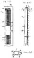
- FIG. I shows a surface-mount type electric connector according to one embodiment of the present device.
- the electric connector comprises a housing 2 which is made of an insulating material and is molded into an integral structure, and a plurality of female terminals 4 which are received in the housing in a state of being mutually insulated and function as an electric contact.
- These plurality of female terminals 4 are collectively driven into the housing 2 by means of an assembling machine (not shown) so that they are arranged at predetermined intervals along a longitudinal direction of the housing 2.
- each female terminal 4 comprises a pair of terminal sections 4a and 4b.
- Each of the terminal sections 4a and 4b has one end portion 6 soldered onto a predetermined position of a printed circuit board B, and the other end portion 8 connecting with a male terminal 10 of a mating connector, and are held in the housing 2 in a state in which a portion between both ends of the terminal section is bent. As shown in the figure, when the male terminal 10 of the mating connector is inserted between the other end portions 8 and 8 of the terminal sections 4a and 4b, an electric connection is made between the connector and the mating connector.
- one end portion 6 of respective terminal sections 4a and 4b are bent outwardly with a predetermined flatness (so as to become parallel with a mount surface of the printed circuit board B), and project into the side of the housing 2, thus forming solder tails to be soldered onto the printed circuit board B.
- Both end sides in the longitudinal direction of the housing 2 are fitted with a hold down member 12 for fixing the electric connector I onto the printed circuit board B so as to cover the female terminal 4 from both sides in the longitudinal direction.
- the hold down member 12 is formed into a thin plate by being subjected to blanking. Further, the hold down member 12 has a convex portion 14 which is fitted into a concave groove 30 provided on the upper portion of the housing 2, and a pair of leg portions 16 and 16 which are formed integrally with the convex portion 14 and fitted along the side face of the housing 2.
- each leg portion 16,16 extends in a manner of being bent into the outside with a predetermined flatness (so as to become parallel with a mount surface of the printed circuit board B), and thus, is formed with a fixed portion 18 to be soldered onto a predetermined position of the printed circuit board B.
- each leg portion 16,16 is formed with a projecting portion 20 projecting toward the side.
- the projecting portion 20 has a projection length which is set so that the projecting portion 20 abuts against a side wall of a receiving groove 50 of a transportation tray T which will be described later. Specifically, a length L, between the projecting portions 20 and 20 is set to the substantially same as a width W (see FIG.
- the housing 2 as a molding product is carried onto a predetermined supply stage by means of a transportation rail, and is fed from the supply stage to an assembling machine. And then, the plurality of female terminals 4 are collectively driven into the housing 2 by means of the assembling machine. In the final stage of the manufacture process, the hold down member 12 is attached onto both sides in the longitudinal direction of the housing 2.
- the hold down member 12 is fitted into the concave groove 30 provided on the upper portion of the housing 2 while its leg portions 16 and 16 being fitted along the side face of the housing 2.
- the bold down member 12 is attached from a direction of substantially converse to an assembly direction of driving the female terminals 4 into the housing 2 (the side converse to the mount surface of the connector 1).
- the assembled connector 1 is transported after being collectively received in a transportation tray T having a plurality of receiving grooves 50 with a predetermined number of articles.
- the electric connector 1 is received in each receiving groove 50 in a state as shown in FIG. 4.
- a bottom face of the receiving groove 50 is formed with a projecting portion 52 along its longitudinal direction.
- the housing 2 of the connector I is raised upward by means of the projecting portion 52, so that the solder tail 6 does not contact with the bottom face of the receiving groove 50; therefore, no stress is applied to the solder tail 6.
- the width W of the receiving groove 50 is set larger than a substantial width of the connector I so that the solder tail 6 does not contact with the side wall of the receiving groove 50.
- the connector I is shaky during transportation.
- the projecting portions 20 and 20 on both sides of the hold down member 12 are abutted against both side walls of the receiving groove 50, so that the connector 1 is accurately positioned in the receiving groove 50; therefore, the shakiness accompanying with rotation and vibration of the connector 1 can be prevented.
- the solder tail 6 and the side wall of the receiving groove 50 is prevented from contact with each other by means of the hold down member 12 covering the female terminals 4 from both sides in its longitudinal direction, thus, tail protection can be securely achieved.
- the connector 1 In an automatic mounting process of automatically mounting the connector 1 onto the printed circuit board B, the connector 1 is sucked up by one from the tray T by means of a specific nozzle, and then, is carried onto the printed circuit board B.
- a Kapton tape 45 (see FIG. 1) made of a polyimide film is stack onto the upper face of the connector 1.
- the Kapton tape 45 is used as an absorption face for sucking up the connector 1 by means of the specific nozzle.
- the connector 1 is situated on a predetermined position on the printed circuit board, and thereafter, is mounted on the printed circuit board B by being subjected to reflow soldering.
- solder tail 6 of the female terminal 4 is soldered to a predetermined position of a printed circuit on the printed circuit board B, and also, the fixed portion 18 of leg portion 16 of the hold down member 12 is soldered to the predetermined position of the printed circuit board B.
- the housing 2 is pressed from its top by means of the hold down member so as to be firmly held on the printed circuit board B.
- the Kapton tape 45 is peeled off from the connector 1 by a user after being subjected to soldering.
- the housing 2 is held down on the printed circuit board B from its top by means of the hold down member 12.
- the hold down member 12 fixes the housing 2 on the printed circuit board B with sufficient hold-down strength, and receives a force acting when drawing out the mating connector from the connector 1 from side opposite to the acting force, so that a stress can be prevented from excessively applying to the solder tail 6 of the female terminal 4.
- the electric connector I sufficiently withstands against the force in a draw-out direction.
- the thin formed hold down member 12 is fitted on both side ends in the longitudinal direction of the housing. For this reason, the hold down member 12 does not project from both sides of the connector 1, so that a space occupied by the connector 1 on the printed circuit board B is smaller as compared with that of a connector disclosed in U.S. Patent No. 5,263,867.
- the hold down member 12 is located so as to cover the female terminal 4 from its both side in the longitudinal direction. Even if the connector 1 is shaky in its longitudinal direction in the receiving groove 50 of the tray T due to vibration during transportation, the hold down member 12 can prevent the solder tail 6 and the side walls of the receiving groove 50 from contacting with each other. Namely, tail protection during transportation can be securely achieved in the longitudinal direction of the connector 1. Furthermore, in the electric connector 1 of this embodiment, the hold down member 12 is provided with the projecting portions 20 which abut against both sides both side walls of the receiving groove 50 of the tray T at its both sides.
- the connector 1 is accurately positioned in the receiving groove 50, so that the connector 1 can be prevented from being rotated and shaky. Namely, tail protection during transportation can be securely achieved in the width direction of the connector 1. Also, since the tray T and the housing 2 are not provided with the projecting portion 20, there is no need of making large a width of the transportation rail for feeding the housing 2 to the assembly machine in the connector manufacture process in accordance with the projecting portion 20. Thus, the tray T is not required having strictly precision. In other words, tail protection during transportation can be improved without causing failure in the connector manufacture process and increasing manufacture cost of the transportation tray T.
- the hold down member 12 is attached to the housing 2, therefore, there is no need of widening the width of the transportation rail and taking specific measures against the connector manufacture machine side even if the hold down member 12 is provided with the aforesaid projecting portions 20.
- the hold down member 12 is formed by being subjected to blanking. Therefore, the.hold down member 12 is formed considerably thin with high dimensional accuracy. As a result, there can be obtained a preferable flatness of the fixed portion 18 of the hold down member 12 soldered onto the surface of the printed circuit board B. Moreover, by making use of the flatness of the solder tail 6, the connector 1 can be mounted on the surface of the printed circuit board B in a preferable state.
- a length L2 between the fixed portions 18 and 18 of the down hold member 12 is set larger than a length L3 between the solder tails 6 and 6 of the female terminal 4.
- the length L2 between the fixed portions 18 and 18 is set at the same as the length L, between the projecting portions 20 and 20, both fixed portion 18 and projecting portion 20 abut against both side walls of the receiving groove 50 of the tray T, so that the connector 1 can be more securely positioned in the receiving groove 50.
- the hold down member 12 may be provided with an engagement portion 25 which is momentarily held in the printed circuit board B.
- the engagement portion 25 is provided in the convex portion 14 of the hold down member 12, and extends downward on the inner side of the hold down member 12.
- the engagement portion 25 extends through a hole 27 penetrating from the concave groove 30 of the housing 2 to the lower face thereof, and projects from the lower face of the housing 2.
- the surface of the lower end portion of the engagement portion 25 is formed with an engagement means which is capable of engaging with a groove 40 formed in the printed circuit board B.
- the engagement means may be, for example, a screw portion formed in the surface of the engagement portion 25, or a fine protrusion formed in the surface of the engagement portion 25.
- the engagement means may of course be any other form so long as the engagement portion 25 can be momentarily held in the groove 40 by friction.
- the connector 1 is not shaky when soldering the female terminal 4 and the fixed portion 18 of the hold down member 12 onto the printed circuit board B; therefore, the soldering operation can be readily achieved. This exhibits the effect when the soldering operation is carried out by manually, and not automatic mounting.
- mounting density on the printed circuit board can be enhanced, and also, tall protection during transportation can be improved without causing failure in the connector manufacture process and increasing manufacture cost of the transportation tray for the connector.
Applications Claiming Priority (3)
| Application Number | Priority Date | Filing Date | Title |
|---|---|---|---|
| JP1997005327U JP3044604U (ja) | 1997-06-20 | 1997-06-20 | 電気コネクタ |
| JP532797U | 1997-06-20 | ||
| JP5327/97U | 1997-06-20 |
Publications (2)
| Publication Number | Publication Date |
|---|---|
| EP0886348A2 true EP0886348A2 (de) | 1998-12-23 |
| EP0886348A3 EP0886348A3 (de) | 1999-11-17 |
Family
ID=11608159
Family Applications (1)
| Application Number | Title | Priority Date | Filing Date |
|---|---|---|---|
| EP98110978A Withdrawn EP0886348A3 (de) | 1997-06-20 | 1998-06-16 | Elektrischer Verbinder |
Country Status (5)
| Country | Link |
|---|---|
| EP (1) | EP0886348A3 (de) |
| JP (1) | JP3044604U (de) |
| KR (1) | KR100545965B1 (de) |
| SG (1) | SG71805A1 (de) |
| TW (1) | TW377922U (de) |
Families Citing this family (1)
| Publication number | Priority date | Publication date | Assignee | Title |
|---|---|---|---|---|
| JP3940387B2 (ja) * | 2003-07-29 | 2007-07-04 | タイコエレクトロニクスアンプ株式会社 | コネクタ組立体 |
Citations (4)
| Publication number | Priority date | Publication date | Assignee | Title |
|---|---|---|---|---|
| US5259789A (en) * | 1993-02-23 | 1993-11-09 | Molex Incorporated | Retention system for circuit board mounted electrical connector |
| US5263867A (en) * | 1991-03-18 | 1993-11-23 | Kel Corporation | Connector with contact locating housing part |
| US5395265A (en) * | 1991-07-16 | 1995-03-07 | Berg Technology, Inc. | Retention system for a connector housing |
| US5411236A (en) * | 1990-12-25 | 1995-05-02 | Hirose Electric Co., Ltd. | Reinforcing metal fitting for surface mount connector |
Family Cites Families (4)
| Publication number | Priority date | Publication date | Assignee | Title |
|---|---|---|---|---|
| JPH06310197A (ja) * | 1993-04-23 | 1994-11-04 | Matsushita Electric Works Ltd | コネクタ |
| JPH07240246A (ja) * | 1994-02-28 | 1995-09-12 | Amp Japan Ltd | 基板実装型電気コネクタ |
| EP0808520B1 (de) * | 1995-02-09 | 1999-04-14 | The Whitaker Corporation | Elektrischer steckverbinder für gedruckte schaltungen |
| JPH097693A (ja) * | 1995-06-14 | 1997-01-10 | Japan Aviation Electron Ind Ltd | コネクタ |
-
1997
- 1997-06-20 JP JP1997005327U patent/JP3044604U/ja not_active Expired - Lifetime
-
1998
- 1998-06-12 TW TW087209400U patent/TW377922U/zh unknown
- 1998-06-16 EP EP98110978A patent/EP0886348A3/de not_active Withdrawn
- 1998-06-18 SG SG1998001459A patent/SG71805A1/en unknown
- 1998-06-19 KR KR1019980023142A patent/KR100545965B1/ko not_active IP Right Cessation
Patent Citations (4)
| Publication number | Priority date | Publication date | Assignee | Title |
|---|---|---|---|---|
| US5411236A (en) * | 1990-12-25 | 1995-05-02 | Hirose Electric Co., Ltd. | Reinforcing metal fitting for surface mount connector |
| US5263867A (en) * | 1991-03-18 | 1993-11-23 | Kel Corporation | Connector with contact locating housing part |
| US5395265A (en) * | 1991-07-16 | 1995-03-07 | Berg Technology, Inc. | Retention system for a connector housing |
| US5259789A (en) * | 1993-02-23 | 1993-11-09 | Molex Incorporated | Retention system for circuit board mounted electrical connector |
Also Published As
| Publication number | Publication date |
|---|---|
| TW377922U (en) | 1999-12-21 |
| KR19990007155A (ko) | 1999-01-25 |
| JP3044604U (ja) | 1998-01-06 |
| EP0886348A3 (de) | 1999-11-17 |
| KR100545965B1 (ko) | 2006-03-23 |
| SG71805A1 (en) | 2000-04-18 |
Similar Documents
| Publication | Publication Date | Title |
|---|---|---|
| KR101151534B1 (ko) | 소켓과 헤더의 결합 상태를 유지하는 록 기구를 구비한 커넥터 및 커넥터의 제조 방법 | |
| EP0459680B1 (de) | Elektrischer Steckverbinder von Leiterplatte zu Leiterplatte mit Stiften und Buchsen von verringertem Teilungsmass | |
| US6287130B1 (en) | Construction and method of connecting connector to base board | |
| CN101901975B (zh) | 连接器组以及在该连接器组中使用的接合器 | |
| JPH08250167A (ja) | Pcカード用コネクタ | |
| JPH10189181A (ja) | プラグコネクタ | |
| US6442036B2 (en) | Substrate mount type terminal | |
| US6135795A (en) | Electrical connector with cover | |
| KR100715015B1 (ko) | 전자부품부착용 소켓 | |
| JPH09153384A (ja) | 電気コネクタ用キャップ | |
| US6955545B1 (en) | Two piece ball grid array | |
| US20220216627A1 (en) | Connector and connector mounting body | |
| US20090156044A1 (en) | Electrical Connector and Contact Insertion Guide | |
| US6716060B2 (en) | Electrical connector with solder plate and pegs for PC board mounting | |
| US5880405A (en) | Terminal structure for electronic part with stepped offset portions | |
| US6050851A (en) | Electric connector | |
| EP0886348A2 (de) | Elektrischer Verbinder | |
| JP4627301B2 (ja) | 表面実装型ヘッダ組立体 | |
| JP2001052788A (ja) | Fpcとプリント基板間の電気コネクタ装置 | |
| US5984722A (en) | Printed board connector | |
| JP2000036338A (ja) | 電気コネクタ | |
| JPH10233268A (ja) | カードバス用コネクタとその表面実装方法 | |
| US11594830B2 (en) | Contact | |
| JPH056759U (ja) | Fpc接続用コネクタ | |
| JPH07326442A (ja) | 表面実装用電気コネクタ |
Legal Events
| Date | Code | Title | Description |
|---|---|---|---|
| PUAI | Public reference made under article 153(3) epc to a published international application that has entered the european phase |
Free format text: ORIGINAL CODE: 0009012 |
|
| AK | Designated contracting states |
Kind code of ref document: A2 Designated state(s): DE FR GB |
|
| AX | Request for extension of the european patent |
Free format text: AL;LT;LV;MK;RO;SI |
|
| PUAL | Search report despatched |
Free format text: ORIGINAL CODE: 0009013 |
|
| AK | Designated contracting states |
Kind code of ref document: A3 Designated state(s): AT BE CH CY DE DK ES FI FR GB GR IE IT LI LU MC NL PT SE |
|
| AX | Request for extension of the european patent |
Free format text: AL;LT;LV;MK;RO;SI |
|
| RIC1 | Information provided on ipc code assigned before grant |
Free format text: 6H 01R 23/70 A, 6H 01R 9/09 B, 6H 01R 23/72 B, 6H 05K 7/12 B |
|
| 17P | Request for examination filed |
Effective date: 20000324 |
|
| AKX | Designation fees paid |
Free format text: DE FR GB |
|
| 17Q | First examination report despatched |
Effective date: 20000724 |
|
| GRAH | Despatch of communication of intention to grant a patent |
Free format text: ORIGINAL CODE: EPIDOS IGRA |
|
| GRAH | Despatch of communication of intention to grant a patent |
Free format text: ORIGINAL CODE: EPIDOS IGRA |
|
| RAP1 | Party data changed (applicant data changed or rights of an application transferred) |
Owner name: FCI |
|
| RIC1 | Information provided on ipc code assigned before grant |
Ipc: 7H 05K 7/12 B Ipc: 7H 01R 12/22 B Ipc: 7H 01R 12/04 B Ipc: 7H 01R 12/18 A |
|
| STAA | Information on the status of an ep patent application or granted ep patent |
Free format text: STATUS: THE APPLICATION IS DEEMED TO BE WITHDRAWN |
|
| 18D | Application deemed to be withdrawn |
Effective date: 20040103 |