EP0884780A2 - Halbleitervorrichtung mit verbesserter Leiter-Chip Haftungsstruktur und zu diesem Zweck eingesetzter Leiterrahmen - Google Patents
Halbleitervorrichtung mit verbesserter Leiter-Chip Haftungsstruktur und zu diesem Zweck eingesetzter Leiterrahmen Download PDFInfo
- Publication number
- EP0884780A2 EP0884780A2 EP98110843A EP98110843A EP0884780A2 EP 0884780 A2 EP0884780 A2 EP 0884780A2 EP 98110843 A EP98110843 A EP 98110843A EP 98110843 A EP98110843 A EP 98110843A EP 0884780 A2 EP0884780 A2 EP 0884780A2
- Authority
- EP
- European Patent Office
- Prior art keywords
- electrically insulative
- insulative adhesive
- inner leads
- semiconductor chip
- adhesive tape
- Prior art date
- Legal status (The legal status is an assumption and is not a legal conclusion. Google has not performed a legal analysis and makes no representation as to the accuracy of the status listed.)
- Withdrawn
Links
Images















Classifications
-
- H—ELECTRICITY
- H10—SEMICONDUCTOR DEVICES; ELECTRIC SOLID-STATE DEVICES NOT OTHERWISE PROVIDED FOR
- H10W—GENERIC PACKAGES, INTERCONNECTIONS, CONNECTORS OR OTHER CONSTRUCTIONAL DETAILS OF DEVICES COVERED BY CLASS H10
- H10W70/00—Package substrates; Interposers; Redistribution layers [RDL]
- H10W70/40—Leadframes
- H10W70/411—Chip-supporting parts, e.g. die pads
- H10W70/415—Leadframe inner leads serving as die pads
-
- H—ELECTRICITY
- H10—SEMICONDUCTOR DEVICES; ELECTRIC SOLID-STATE DEVICES NOT OTHERWISE PROVIDED FOR
- H10W—GENERIC PACKAGES, INTERCONNECTIONS, CONNECTORS OR OTHER CONSTRUCTIONAL DETAILS OF DEVICES COVERED BY CLASS H10
- H10W70/00—Package substrates; Interposers; Redistribution layers [RDL]
- H10W70/40—Leadframes
- H10W70/421—Shapes or dispositions
-
- H—ELECTRICITY
- H10—SEMICONDUCTOR DEVICES; ELECTRIC SOLID-STATE DEVICES NOT OTHERWISE PROVIDED FOR
- H10W—GENERIC PACKAGES, INTERCONNECTIONS, CONNECTORS OR OTHER CONSTRUCTIONAL DETAILS OF DEVICES COVERED BY CLASS H10
- H10W72/00—Interconnections or connectors in packages
- H10W72/50—Bond wires
-
- H—ELECTRICITY
- H10—SEMICONDUCTOR DEVICES; ELECTRIC SOLID-STATE DEVICES NOT OTHERWISE PROVIDED FOR
- H10W—GENERIC PACKAGES, INTERCONNECTIONS, CONNECTORS OR OTHER CONSTRUCTIONAL DETAILS OF DEVICES COVERED BY CLASS H10
- H10W90/00—Package configurations
- H10W90/811—Multiple chips on leadframes
-
- H—ELECTRICITY
- H10—SEMICONDUCTOR DEVICES; ELECTRIC SOLID-STATE DEVICES NOT OTHERWISE PROVIDED FOR
- H10W—GENERIC PACKAGES, INTERCONNECTIONS, CONNECTORS OR OTHER CONSTRUCTIONAL DETAILS OF DEVICES COVERED BY CLASS H10
- H10W72/00—Interconnections or connectors in packages
- H10W72/01—Manufacture or treatment
- H10W72/015—Manufacture or treatment of bond wires
-
- H—ELECTRICITY
- H10—SEMICONDUCTOR DEVICES; ELECTRIC SOLID-STATE DEVICES NOT OTHERWISE PROVIDED FOR
- H10W—GENERIC PACKAGES, INTERCONNECTIONS, CONNECTORS OR OTHER CONSTRUCTIONAL DETAILS OF DEVICES COVERED BY CLASS H10
- H10W72/00—Interconnections or connectors in packages
- H10W72/071—Connecting or disconnecting
- H10W72/075—Connecting or disconnecting of bond wires
- H10W72/07511—Treating the bonding area before connecting, e.g. by applying flux or cleaning
-
- H—ELECTRICITY
- H10—SEMICONDUCTOR DEVICES; ELECTRIC SOLID-STATE DEVICES NOT OTHERWISE PROVIDED FOR
- H10W—GENERIC PACKAGES, INTERCONNECTIONS, CONNECTORS OR OTHER CONSTRUCTIONAL DETAILS OF DEVICES COVERED BY CLASS H10
- H10W72/00—Interconnections or connectors in packages
- H10W72/50—Bond wires
- H10W72/531—Shapes of wire connectors
- H10W72/536—Shapes of wire connectors the connected ends being ball-shaped
-
- H—ELECTRICITY
- H10—SEMICONDUCTOR DEVICES; ELECTRIC SOLID-STATE DEVICES NOT OTHERWISE PROVIDED FOR
- H10W—GENERIC PACKAGES, INTERCONNECTIONS, CONNECTORS OR OTHER CONSTRUCTIONAL DETAILS OF DEVICES COVERED BY CLASS H10
- H10W72/00—Interconnections or connectors in packages
- H10W72/50—Bond wires
- H10W72/531—Shapes of wire connectors
- H10W72/5363—Shapes of wire connectors the connected ends being wedge-shaped
-
- H—ELECTRICITY
- H10—SEMICONDUCTOR DEVICES; ELECTRIC SOLID-STATE DEVICES NOT OTHERWISE PROVIDED FOR
- H10W—GENERIC PACKAGES, INTERCONNECTIONS, CONNECTORS OR OTHER CONSTRUCTIONAL DETAILS OF DEVICES COVERED BY CLASS H10
- H10W72/00—Interconnections or connectors in packages
- H10W72/50—Bond wires
- H10W72/541—Dispositions of bond wires
- H10W72/5445—Dispositions of bond wires being orthogonal to a side surface of the chip, e.g. parallel arrangements
-
- H—ELECTRICITY
- H10—SEMICONDUCTOR DEVICES; ELECTRIC SOLID-STATE DEVICES NOT OTHERWISE PROVIDED FOR
- H10W—GENERIC PACKAGES, INTERCONNECTIONS, CONNECTORS OR OTHER CONSTRUCTIONAL DETAILS OF DEVICES COVERED BY CLASS H10
- H10W72/00—Interconnections or connectors in packages
- H10W72/851—Dispositions of multiple connectors or interconnections
- H10W72/853—On the same surface
- H10W72/865—Die-attach connectors and bond wires
-
- H—ELECTRICITY
- H10—SEMICONDUCTOR DEVICES; ELECTRIC SOLID-STATE DEVICES NOT OTHERWISE PROVIDED FOR
- H10W—GENERIC PACKAGES, INTERCONNECTIONS, CONNECTORS OR OTHER CONSTRUCTIONAL DETAILS OF DEVICES COVERED BY CLASS H10
- H10W72/00—Interconnections or connectors in packages
- H10W72/851—Dispositions of multiple connectors or interconnections
- H10W72/874—On different surfaces
- H10W72/884—Die-attach connectors and bond wires
-
- H—ELECTRICITY
- H10—SEMICONDUCTOR DEVICES; ELECTRIC SOLID-STATE DEVICES NOT OTHERWISE PROVIDED FOR
- H10W—GENERIC PACKAGES, INTERCONNECTIONS, CONNECTORS OR OTHER CONSTRUCTIONAL DETAILS OF DEVICES COVERED BY CLASS H10
- H10W74/00—Encapsulations, e.g. protective coatings
-
- H—ELECTRICITY
- H10—SEMICONDUCTOR DEVICES; ELECTRIC SOLID-STATE DEVICES NOT OTHERWISE PROVIDED FOR
- H10W—GENERIC PACKAGES, INTERCONNECTIONS, CONNECTORS OR OTHER CONSTRUCTIONAL DETAILS OF DEVICES COVERED BY CLASS H10
- H10W74/00—Encapsulations, e.g. protective coatings
- H10W74/10—Encapsulations, e.g. protective coatings characterised by their shape or disposition
- H10W74/131—Encapsulations, e.g. protective coatings characterised by their shape or disposition the semiconductor body being only partially enclosed
- H10W74/142—Encapsulations, e.g. protective coatings characterised by their shape or disposition the semiconductor body being only partially enclosed the encapsulations exposing the passive side of the semiconductor body
-
- H—ELECTRICITY
- H10—SEMICONDUCTOR DEVICES; ELECTRIC SOLID-STATE DEVICES NOT OTHERWISE PROVIDED FOR
- H10W—GENERIC PACKAGES, INTERCONNECTIONS, CONNECTORS OR OTHER CONSTRUCTIONAL DETAILS OF DEVICES COVERED BY CLASS H10
- H10W90/00—Package configurations
- H10W90/701—Package configurations characterised by the relative positions of pads or connectors relative to package parts
- H10W90/731—Package configurations characterised by the relative positions of pads or connectors relative to package parts of die-attach connectors
- H10W90/736—Package configurations characterised by the relative positions of pads or connectors relative to package parts of die-attach connectors between a chip and a stacked lead frame, conducting package substrate or heat sink
-
- H—ELECTRICITY
- H10—SEMICONDUCTOR DEVICES; ELECTRIC SOLID-STATE DEVICES NOT OTHERWISE PROVIDED FOR
- H10W—GENERIC PACKAGES, INTERCONNECTIONS, CONNECTORS OR OTHER CONSTRUCTIONAL DETAILS OF DEVICES COVERED BY CLASS H10
- H10W90/00—Package configurations
- H10W90/701—Package configurations characterised by the relative positions of pads or connectors relative to package parts
- H10W90/751—Package configurations characterised by the relative positions of pads or connectors relative to package parts of bond wires
- H10W90/756—Package configurations characterised by the relative positions of pads or connectors relative to package parts of bond wires between a chip and a stacked lead frame, conducting package substrate or heat sink
Definitions
- the present invention relates to a semiconductor device with an improved lead-hip adhesion structure and a lead frame, and more particularly to a semiconductor device with a lead-on-chip structure and a lead frame to be used therefor.
- FIG. 1 is a fragmentary cross sectional elevation view illustrative of a conventional lead-on-chip structure of a semiconductor device.
- Inner leads 1 extend over a top surface of a semiconductor chip 4.
- the inner leads 1 have stitch portions 2 at inside edges thereof.
- An insulative adhesive tape 3 is adhered with bottom surfaces of the stitch portions 2 of the inner leads 1 aligned in the left side.
- Another insulative adhesive tape 3 is adhered with bottom surfaces of the stitch portions 2 of the inner leads 1 aligned in the right side.
- Each of the insulative adhesive tapes 3 has both surfaces on which an insulative adhesive agent has been applied.
- each of the insulative adhesive tapes 3 has both surfaces on which adhesive layers have been formed.
- the inner leads 1 extend toward a center line of the semiconductor chip 4.
- the semiconductor chip 4 is bonded or adhered with the bottom surfaces of the insulative adhesive tapes 3, wherein the insulative adhesive tapes 3 have already been adhered to the bottom surfaces of the stitch portions 2 of the inner leads 1.
- the semiconductor chip 4 has two alignments of bonding pads 10 along the center line so that individual bonding pads correspond to individual inner leads 1 as illustrated in FIG. 2.
- the two alignments of bonding pads 10 of the semiconductor chip 4 are positioned inside of the stitch portions 2 of the inner leads 1 and also the insulative adhesive tapes 3.
- the stitch portion 2 of the inner lead 1 is bonded through a bonding wire 5 to the corresponding bonding pad 10 formed on the semiconductor chip 4 so that the inner leads 1 are electrically connected through the bonding wires 5 to the corresponding bonding pads 10 formed on the semiconductor chip 4.
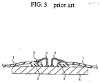
- FIG. 3 is a fragmentary cross sectional elevation view illustrative of the above conventional lead-on-chip structure of the semiconductor device, wherein inner leads are in contact with edges of the semiconductor chip 4 to describe a first problem with the above conventional lead-on-chip structure.
- the inner leads 1 are fixed at the stitch portions 2 by the insulative adhesive tapes 3 but other portions of the inner leads 1 positioned outside of the stitch portions 2 are not fixed.
- the semiconductor chip 4 is mounted on a printed circuit board by use of a sealing resin wherein a heat is applied to the semiconductor chip 4 and the inner leads 1.
- the insulative adhesive tapes 3 have a different thermal expansion coefficient from that of the sealing resin, for which reason a stress is generated by the difference in thermal expansion coefficient between the insulative adhesive tapes 3 and the sealing resin.
- the stress is applied between the insulative adhesive tapes 3 and the sealing resin, whereby a pealing may be generated between the insulative adhesive tapes 3 and the sealing resin.
- it is effective to narrow the width of the insulative adhesive tapes 3 as much as possible.
- a pair of possible slender insulative adhesive tapes 3 are provided so that when the semiconductor chip 4 has been bonded to the bottom surfaces of the insulative adhesive tapes 3, the possible slender insulative adhesive tapes 3 are positioned along the two alignments of the bonding pads 10 formed on the semiconductor chip 4 as closely to the two alignments of the bonding pads 10, so as to shorten the length of the individual bonding wires 10.
- the long bonding wires have a problem with unstability in shape thereof and also is likely to be deformed by a flow of molten sealing resin when the sealing resin is injected thereunto. For those reasons, it is preferable to shorten the length of the bonding wire 10.
- the stitch portion 2 of the inner lead 1 is positioned as closely to the bonding pad 10 provided close to the center line of the semiconductor chip 4 as possible.
- the long part of the inner lead 1 positioned outside of the stitch portion 2 is not fixed by the insulative adhesive tapes 3. Namely, the long inner lead 1 extending over the semiconductor chip 4 is fixed only at the stitch portion 2 thereof by the slender insulative adhesive tape 3.
- the inner lead 1 might be made into contact with the edge of the semiconductor chip 4. The likelihood of contact between the inner lead 1 and the edge of the semiconductor chip 4 is high as the size of the semiconductor chip 4 is large.
- the above conventional lead-on-chip structure of the semiconductor device is further engaged with a second problem with likelihood of exposure of the tops of the bonding wires 5 or the bottom surface of the semiconductor chip 4 from the sealing resin even after the semiconductor device has been packaged with the sealing resin.
- the long part of the individual inner lead 1 extends over the semiconductor chip 4 and is not fixed by the slender insulative adhesive tape 3. This allows the semiconductor chip 4 to move or displace in a direction vertical to the surface of the semiconductor chip 4 by the pressure of the sealing resin injected into dies for molding the semiconductor device.
- FIG. 4A is a fragmentary cross sectional elevation view illustrative of a semiconductor package, wherein the semiconductor chip 4 has been moved upwardly by the pressure of the sealing resin injected into the dies and the tops of the bonding wires 5 are shown from the sealing resin.
- FIG. 4B is a fragmentary cross sectional elevation view illustrative of a semiconductor package, wherein the semiconductor chip 4 has been moved downwardly by the pressure of the sealing resin injected into the dies and the bottom surface of the semiconductor chip 4 is shown from the sealing resin.
- the above lead-on-chip structure is also engaged with the following third problem. Even if the tops of the bonding wires 5 or the bottom of the semiconductor chip 4 are not exposed from the sealing resin, movement or shift in vertical direction to the surface of the semiconductor chip 4 results in variation in thickness of the resin from predetermined thicknesses. A balance is lost in thickness between an upper portion of the resin overlying the semiconductor chip 4 and a lower portion of the resin underlying the semiconductor chip 4. As a result, the semiconductor package may be bent or arched. Further, a reduction in thickness of the upper or lower portion of the resin results in a drop of strength. If a stress is concentrated into the thickness-reduced portion of the resin, a crack is likely to appear on the thickness-reduced portion of the resin.
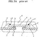
- FIG. 5A is a fragmentary cross sectional elevation view illustrative of a conventional chip-on-lead structure of a semiconductor device.
- Inner leads 1 extend under a bottom surface of a semiconductor chip 4.
- the inner leads 1 have stitch portions 2 at inside edges thereof.
- An insulative adhesive tape 3 is adhered with top surfaces of the stitch portions 2 of the inner leads 1 aligned in the left side.
- Another insulative adhesive tape 3 is adhered with top surfaces of the stitch portions 2 of the inner leads 1 aligned in the right side.
- Each of the insulative adhesive tapes 3 has both surfaces on which an insulative adhesive agent has been applied.
- each of the insulative adhesive tapes 3 has both surfaces on which adhesive layers have been formed.
- the inner leads 1 extend toward a center line of the semiconductor chip 4.
- the semiconductor chip 4 is bonded or adhered with the top surfaces of the insulative adhesive tapes 3, wherein the insulative adhesive tapes 3 have already been adhered to the top surfaces of the stitch portions 2 of the inner leads 1.
- the semiconductor chip 4 has two alignments of bonding pads 10 along opposite sides of the semiconductor chip 4 so that individual bonding pads 10 correspond to individual inner leads 1.
- the stitch portion 2 of the inner lead 1 is bonded through a bonding wire 5 to the corresponding bonding pad 10 formed on the top surface of the semiconductor chip 4 so that the inner leads 1 are electrically connected through the bonding wires 5 to the corresponding bonding pads 10.
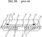
- FIG. 5B is a fragmentary cross sectional elevation view illustrative of the above conventional lead-on-chip structure of the semiconductor device, wherein inner leads 1 are in contact with edges of the semiconductor chip 4 to describe the same problem as engaged with the above conventional lead-on-chip structure.
- the inner leads 1 are fixed at the stitch portions 2 by the insulative adhesive tapes 3 but other portions of the inner leads 1 positioned outside of the stitch portions 2 are not fixed.
- the semiconductor chip 4 is mounted on a printed circuit board by use of a sealing resin wherein a heat is applied to the semiconductor chip 4 and the inner leads 1.
- the insulative adhesive tapes 3 have a different thermal expansion coefficient from that of the sealing resin, for which reason a stress is generated by the difference in thermal expansion coefficient between the insulative adhesive tapes 3 and the sealing resin.
- the stress is applied between the insulative adhesive tapes 3 and the sealing resin, whereby a pealing may be generated between the insulative adhesive tapes 3 and the sealing resin.
- it is effective to narrow the width of the insulative adhesive tapes 3 as much as possible.
- a pair of possible slender insulative adhesive tapes 3 are provided so that when the semiconductor chip 4 has been bonded to the bottom surfaces of the insulative adhesive tapes 3, the possible slender insulative adhesive tapes 3 are positioned relatively close to the center line of the semiconductor chip 4. This results in that a long part of the inner lead 1 positioned outside of the stitch portion 2 extends over the semiconductor chip 4. This is remarkable as the size of the semiconductor chip 4 becomes large.
- the long part of the inner lead 1 positioned outside of the stitch portion 2 is not fixed by the insulative adhesive tapes 3. Namely, the long inner lead 1 extending over the semiconductor chip 4 is fixed only at the stitch portion 2 thereof by the slender insulative adhesive tape 3.
- the inner lead 1 might be made into contact with the edge of the semiconductor chip 4.
- the likelihood of contact between the inner lead 1 and the edge of the semiconductor chip 4 is high as the size of the semiconductor chip 4 is large.
- the above conventional lead-on-chip structure of the semiconductor device is further engaged with a second problem with likelihood of exposure of the tops of the bonding wires 5 or the bottom surface of the stitched portion 2 of the inner lead 1 from the sealing resin even after the semiconductor device has been packaged with the sealing resin.
- the long part of the individual inner lead 1 extends under the semiconductor chip 4 and is not fixed by the slender insulative adhesive tape 3. This allows the semiconductor chip 4 to move or displace in a direction vertical to the surface of the semiconductor chip 4 by the pressure of the sealing resin injected into dies for molding the semiconductor device.
- the above chip-on-lead structure is also engaged with the following third problem. Even if the tops of the bonding wires 5 or the bottom of the stitched portions 2 of the inner leads 1 are not exposed from the sealing resin, movement or shift in vertical direction to the surface of the semiconductor chip 4 results in variation in thickness of the resin from predetermined thicknesses. A balance is lost in thickness between an upper portion of the resin overlying the semiconductor chip 4 and a lower portion of the resin underlying the semiconductor chip 4. As a result, the semiconductor package may be bent or arched. Further, a reduction in thickness of the upper or lower portion of the resin results in a drop of strength. If a stress is concentrated into the thickness-reduced portion of the resin, a crack is likely to appear on the thickness-reduced portion of the resin.
- the first present invention provides an adhering structure between a semiconductor chip and two alignments of first side inner leads and second side inner leads extending in first and second sides of the semiconductor chip respectively.
- Each of the first and second side inner leads has a stitched portion.
- the first and second sides are separated by a center line of the semiconductor chip.
- the semiconductor chip and the first and second side inner leads are adhered to each other by first and second side electrically insulative adhesive tapes respectively.
- Each of the first and second side electrically insulative adhesive tapes has both surfaces with adhesion force.
- the first and second side electrically insulative adhesive tapes extend on first and second inner stripe regions so as to adhere the stitched portions of the first and second side inner leads respectively.
- each of the first and second side electrically insulative adhesive tapes is further present in at least two positions which are spaced from each other in a direction parallel to the center line and which are also located in the vicinity of an edge of the semiconductor chip, where the edge extends substantially in parallel to the center line, so that the inner leads, which extend through the two positions, are also fixed in the vicinity of the edge of the semiconductor chip.
- the semiconductor chip and the inner leads aligned are fixed by the electrically insulative adhesive tape at a plurality of positions which are distanced from each other to keep a positional balance of fixing points so as to certainly prevent the any substantive movement of the semiconductor chip particularly in the direction vertical to the surface of the semiconductor chip.
- the presence of the electrically insulative adhesive tape at least the two positions spaced from each other in the direction parallel to the center line and which are also located in the vicinity of the edge of the semiconductor chip would result in that inner leads, which extend through the two positions, are fixed not only at the stitched portion but also outside portion in the vicinity of the edge of the semiconductor chip.
- This structure is capable of certainly preventing a substantive movement of the semiconductor chip in a direction vertical to the surface of the semiconductor chip by pressure of the flow of the molten resin when the resin is injected into dies for packaging the semiconductor chip.
- the certain prevention of the substantive movement of the semiconductor chip would result in a certain prevention of the inner leads from being made into contact with the edge of the semiconductor chip.
- the certain prevention of the substantive movement of the semiconductor chip would also result in a certain prevention of the top portion of the semiconductor device such as tops of bonding wires from exposure from the sealing resin.
- the certain prevention of the substantive movement of the semiconductor chip would also result in a certain prevention of the bottom portion of the semiconductor device such as bottom surface of the semiconductor chip or the inner leads from exposure from the sealing resin.
- the certain prevention of the substantive movement of the semiconductor chip means that the above structure is also capable of keeping a constant distance between the semiconductor chip and the inner lead extending over the semiconductor chip.
- the certain prevention of the substantive movement of the semiconductor chip also means that the structure is capable of keeping a balance in thickness between upper and lower portions of the sealing resin packaging the semiconductor chip due to no substantive movement nor shift in the direction vertical to the surface of the semiconductor chip. Keeping the balance in thickness between upper and lower portions of the scaling resin prevents formation of any thickness-reduced portion, resulting in a remarkable reduction in the probability in appearance of crack on the thickness-reduced portion of the resin. From the above description, it can be understood that the above novel structure allows a high yield of manufacturing the semiconductor device and also allows the semiconductor device to have a high reliability.
- FIG. 1 is a fragmentary cross sectional elevation view illustrative of a conventional lead-on-chip structure of a semiconductor device.
- FIG. 2 is a schematic plane view illustrative of a semiconductor chip on which a pair of slender stripe adhesive tapes are provided along just opposite outsides of two alignments of bonding pads provided on the semiconductor chip.
- FIG. 3 is a fragmentary cross sectional elevation view illustrative of the above conventional lead-on-chip structure of the semiconductor device, wherein inner leads are in contact with edges of the semiconductor chip to describe the first problem with the above conventional lead-on-chip structure.
- FIG. 4A is a fragmentary cross sectional elevation view illustrative of a semiconductor package, wherein the semiconductor chip has been moved upwardly by the pressure of the sealing resin injected into the dies and the tops of the bonding wires are shown from the sealing resin.
- FIG. 4B is a fragmentary cross sectional elevation view illustrative of a semiconductor package, wherein the semiconductor chip has been moved downwardly by the pressure of the sealing resin injected into the dies and the bottom surface of the semiconductor chip is shown from the sealing resin.
- FIG. 5A is a fragmentary cross sectional elevation view illustrative of a conventional chip-on-lead structure of the semiconductor device.
- FIG. 5B is a fragmentary cross sectional elevation view illustrative of the above conventional lead-on-chip structure of the semiconductor device, wherein inner leads are in contact with edges of the semiconductor chip to describe the same problem as engaged with the above conventional lead-on-chip structure.
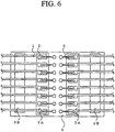
- FIG. 6 is a fragmentary plane view illustrative of a novel lead-on-chip structure of a semiconductor device in a first embodiment in accordance with the present invention.
- FIG. 7 is a fragmentary cross sectional elevation view illustrative of a novel lead-on-chip structure of a semiconductor device in a first embodiment in accordance with the present invention.
- FIG. 8 is a fragmentary cross sectional elevation view illustrative of a novel lead-on-chip structure semiconductor device packaged with a sealing resin wherein a semiconductor chip had received up-force by a molten resin when the resin was injected into dies in a first embodiment in accordance with the present invention.
- FIG. 9 is a fragmentary cross sectional elevation view illustrative of a novel lead-on-chip structure semiconductor device packaged with a sealing resin wherein a semiconductor chip had received down-force by a molten resin when the resin was injected into dies in a first embodiment in accordance with the present invention.
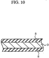
- FIG. 10 is a fragmentary cross sectional elevation view illustrative of an electrically insulative adhesive tape to be used for adhering a semiconductor chip to inner leads in accordance with the present invention.
- FIG. 11 is a fragmentary plane view illustrative of a novel lead-on-chip structure of a semiconductor device in a second embodiment in accordance with the present invention.
- FIG. 12 is a fragmentary plane view illustrative of a novel lead-on-chip structure of a semiconductor device in a third embodiment in accordance with the present invention.
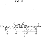
- FIG. 13 is a fragmentary cross sectional elevation view illustrative of a novel lead-on-chip structure of a semiconductor device in a third embodiment in accordance with the present invention.
- FIG. 14 is a fragmentary cross sectional elevation view illustrative of a novel lead-on-chip structure semiconductor device packaged with a sealing resin wherein a semiconductor chip had received up-force by a molten resin when the resin was injected into dies in a third embodiment in accordance with the present invention.
- FIG. 15 is a fragmentary cross sectional elevation view illustrative of a novel lead-on-chip structure semiconductor device packaged with a sealing resin wherein a semiconductor chip had received down-force by a molten resin when the resin was injected into dies in a third embodiment in accordance with the present invention.
- FIG. 16 is a fragmentary plane view illustrative of a novel lead-on-chip structure of a semiconductor device in a fourth embodiment in accordance with the present invention.
- FIG. 17 is a fragmentary plane view illustrative of a novel lead-on-chip structure of a semiconductor device in a fifth embodiment in accordance with the present invention.
- FIG. 18 is a fragmentary cross sectional elevation view illustrative of a novel lead-on-chip structure of a semiconductor device in a fifth embodiment in accordance with the present invention.
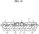
- FIG. 19 is a fragmentary cross sectional elevation view illustrative of a novel lead-on-chip structure semiconductor device packaged with a sealing resin wherein a semiconductor chip had received up-force by a molten resin when the resin was injected into dies in a fifth embodiment in accordance with the present invention.
- FIG. 20 is a fragmentary cross sectional elevation view illustrative of a novel lead-on-chip structure semiconductor device packaged with a sealing resin wherein a semiconductor chip had received down-force by a molten resin when the resin was injected into dies in a fifth embodiment in accordance with the present invention.
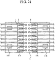
- FIG. 21 is a fragmentary plane view illustrative of a novel lead-on-chip structure of a semiconductor device in a sixth embodiment in accordance with the present invention.
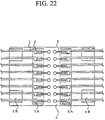
- FIG. 22 is a fragmentary plane view illustrative of a novel lead-on-chip structure of a semiconductor device in a seventh embodiment in accordance with the present invention.
- FIG. 23 is a fragmentary cross sectional elevation view illustrative of a novel lead-on-chip structure of a semiconductor device in a seventh embodiment in accordance with the present invention.
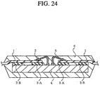
- FIG. 24 is a fragmentary cross sectional elevation view illustrative of a novel lead-on-chip structure semiconductor device packaged with a sealing resin wherein a semiconductor chip had received up-force by a molten resin when the resin was injected into dies in a seventh embodiment in accordance with the present invention.
- FIG. 25 is a fragmentary cross sectional elevation view illustrative of a novel lead-on-chip structure semiconductor device packaged with a sealing resin wherein a semiconductor chip had received down-force by a molten resin when the resin was injected into dies in a seventh embodiment in accordance with the present invention.
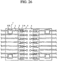
- FIG. 26 is a fragmentary plane view illustrative of a novel lead-on-chip structure of a semiconductor device in an eighth embodiment in accordance with the present invention.
- FIG. 27 is a fragmentary plane view illustrative of a novel lead-on-chip structure of a semiconductor device in a ninth embodiment in accordance with the present invention.
- FIG 28 is a fragmentary plane view illustrative of a novel lead-on-chip structure of a semiconductor device in a tenth embodiment in accordance with the present invention.
- FIG. 29 is a fragmentary plane view illustrative of a novel lead-on-chip structure of a semiconductor device in an eleventh embodiment in accordance with the present invention.
- FIG. 30 is a fragmentary cross sectional elevation view illustrative of a novel lead-on-chip structure of a semiconductor device in an eleventh embodiment in accordance with the present invention.
- FIG. 31 is a fragmentary cross sectional elevation view illustrative of a novel lead-on-chip structure semiconductor device packaged with a sealing resin wherein a semiconductor chip had received up-force by a molten resin when the resin was injected into dies in an eleventh embodiment in accordance with the present invention.
- FIG. 32 is a fragmentary cross sectional elevation view illustrative of a novel lead-on-chip structure semiconductor device packaged with a sealing resin wherein a semiconductor chip had received down-force by a molten resin when the resin was injected into dies in an eleventh embodiment in accordance with the present invention.
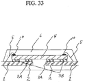
- FIG. 33 is a fragmentary cross sectional elevation view illustrative of a novel chip-on-lead structure of a semiconductor device in a twelfth embodiment in accordance with the present invention.
- the first present invention provides an adhering structure between a semiconductor chip and two alignments of first side inner leads and second side inner leads extending in first and second sides of the semiconductor chip respectively.
- Each of the first and second side inner leads has a stitched portion.
- the first and second sides are separated by a center line of the semiconductor chip.
- the semiconductor chip and the first and second side inner leads are adhered to each other by first and second side electrically insulative adhesive tapes respectively.
- Each of the first and second side electrically insulative adhesive tapes has both surfaces with adhesion force.
- the first and second side electrically insulative adhesive tapes extend on first and second inner stripe regions so as to adhere the stitched portions of the first and second side inner leads respectively.
- each of the first and second side electrically insulative adhesive tapes is further present in at least two positions which are spaced from each other in a direction parallel to the center line and which are also located in the vicinity of an edge of the semiconductor chip, where the edge extends substantially in parallel to the center line, so that the inner leads, which extend through the two positions, are also fixed in the vicinity of the edge of the semiconductor chip.
- the semiconductor chip and the inner leads aligned are fixed by the electrically insulative adhesive tape at a plurality of positions which are distanced from each other to keep a positional balance of fling points so as to certainly prevent the any substantive movement of the semiconductor chip particularly in the direction vertical to the surface of the semiconductor chip.
- the presence of the electrically insulative adhesive tape at least the two positions spaced from each other in the direction parallel to the center line and which are also located in the vicinity of the edge of the semiconductor chip would result in that inner leads, which extend through the two positions, are fixed not only at the stitched portion but also outside portion in the vicinity of the edge of the semiconductor chip.
- This structure is capable of certainly preventing a substantive movement of the semiconductor chip in a direction vertical to the surface of the semiconductor chip by pressure of the flow of the molten resin when the resin is injected into dies for packaging the semiconductor chip.
- the certain prevention of the substantive movement of the semiconductor chip would result in a certain prevention of the inner leads from being made into contact with the edge of the semiconductor chip.
- the certain prevention of the substantive movement of the semiconductor chip would also result in a certain prevention of the top portion of the semiconductor device such as tops of bonding wires from exposure from the sealing resin.
- the certain prevention of the substantive movement of the semiconductor chip would also result in a certain prevention of the bottom portion of the semiconductor device such as bottom surface of the semiconductor chip or the inner leads from exposure from the sealing resin.
- the certain prevention of the substantive movement of the semiconductor chip means that the above structure is also capable of keeping a constant distance between the semiconductor chip and the inner lead extending over the semiconductor chip.
- the certain prevention of the substantive movement of the semiconductor chip also means that the structure is capable of keeping a balance in thickness between upper and lower portions of the sealing resin packaging the semiconductor chip due to no substantive movement nor shift in the direction vertical to the surface of the semiconductor chip. Keeping the balance in thickness between upper and lower portions of the sealing resin prevents formation of any thickness-reduced portion, resulting in a remarkable reduction in the probability in appearance of crack on the thickness-reduced portion of the resin. From the above description, it can be understood that the above novel structure allows a high yield of manufacturing the semiconductor device and also allows the semiconductor device to have a high reliability.
- each of the first and second side electrically insulative adhesive tapes is further positioned so as to adhere outer-most two of the inner leads.
- the outer-most two of the inner leads have spread portions which are adhered with the electrically insulative adhesive tape, so as to increase an adhering area between the inner leads and the electrically insulative adhesive tape and decrease a contact area between the electrically insulative adhesive tape with a sealing resin material for packaging the semiconductor chip. If an adhesion force of the electrically insulative adhesive tape with the sealing resin is relatively weak, it is particularly effective to reduce the contact area between the electrically insulative adhesive tape and the sealing resin for obtaining a high fixing force between the semiconductor chip and the sealing resin.
- each of the first and second side electrically insulative adhesive tapes is further positioned so as to adhere secondly outer two of the inner leads.
- the secondly outer two of the inner leads have spread portions which are adhered with the electrically insulative adhesive tape, so as to increase an adhering area between the inner leads and the electrically insulative adhesive tape and decrease a contact area between the electrically insulative adhesive tape with a sealing resin material for packaging the semiconductor chip. If an adhesion force of the electrically insulative adhesive tape with the sealing resin is relatively weak, it is particularly effective to reduce the contact area between the electrically insulative adhesive tape and the sealing resin for obtaining a high fixing force between the semiconductor chip and the sealing resin.
- each of the first and second side electrically insulative adhesive tapes is further positioned so as to adhere outer-most two and secondly outer two of the inner leads.
- the outer-most two and the secondly outer two of the inner leads have spread portions which are adhered with the electrically insulative adhesive tape, so as to increase an adhering area between the inner leads and the electrically insulative adhesive tape and decrease a contact area between the electrically insulative adhesive tape with a sealing resin material for packaging the semiconductor chip. If an adhesion force of the electrically insulative adhesive tape with the sealing resin is relatively weak, it is particularly effective to reduce the contact area between the electrically insulative adhesive tape and the sealing resin for obtaining a high fixing force between the semiconductor chip and the sealing resin.
- each of the first and second side electrically insulative adhesive tapes is further positioned so as to adhere outer-most one of the inner leads and secondly outer one in an opposite side to the outer-most one.
- the outer-most one of the inner leads and the secondly outer one in an opposite side to the outer-most one of the inner leads have spread portions which are adhered with the electrically insulative adhesive tape, so as to increase an adhering area between the inner leads and the electrically insulative adhesive tape and decrease a contact area between the electrically insulative adhesive tape with a sealing resin material for packaging the semiconductor chip. If an adhesion force of the electrically insulative adhesive tape with the sealing resin is relatively weak, it is particularly effective to reduce the contact area between the electrically insulative adhesive tape and the sealing resin for obtaining a high fixing force between the semiconductor chip and the scaling resin.
- each of the first and second side electrically insulative adhesive tapes further extends on an outer stripe region in the vicinity of and in parallel to the edge of the semiconductor chip, where the outer stripe region is separated from the inner stripe region, and an outside edge of the each of the first and second side electrically insulative adhesive tapes is positioned inside of the edge of the semiconductor chip.
- the inner leads have spread portions which are adhered with the electrically insulative adhesive tape, provided that the spread portions of the adjacent two of the inner leads are separated from each other, so as to increase an adhering area between the inner leads and the electrically insulative adhesive tape and decrease a contact area between the electrically insulative adhesive tape with a sealing resin material for packaging the semiconductor chip. If an adhesion force of the electrically insulative adhesive tape with the sealing resin is relatively weak, it is particularly effective to reduce the contact area between the electrically insulative adhesive tape and the sealing resin for obtaining a high fixing force between the semiconductor chip and the sealing resin.
- each of the first and second side electrically insulative adhesive tapes further extends on an outer stripe region along the edge of the semiconductor chip, where the outer stripe region is separated from the inner stripe region, and an outside edge of the each of the first and second side electrically insulative adhesive tapes is positioned in correspondence to the edge of the semiconductor chip.
- the inner leads have spread portions which are adhered with the electrically insulative adhesive tape, provided that the spread portions of the adjacent two of the inner leads are separated from each other, so as to increase an adhering area between the inner leads and the electrically insulative adhesive tape and decrease a contact area between the electrically insulative adhesive tape with a sealing resin material for packaging the semiconductor chip. If an adhesion force of the electrically insulative adhesive tape with the sealing resin is relatively weak, it is particularly effective to reduce the contact area between the electrically insulative adhesive tape and the sealing resin for obtaining a high fixing force between the semiconductor chip and the sealing resin.
- each of the first and second side electrically insulative adhesive tapes continuously extends from the inner stripe region to the outer stripe region in the vicinity of and in parallel to the edge of the semiconductor chip so that an outside edge of the each of the first and second side electrically insulative adhesive tapes is positioned inside of the edge of the semiconductor chip. If an adhesion force of the electrically insulative adhesive tape with the sealing resin is sufficiently strong, there is raised no problem with increase in contact area between the electrically insulative adhesive tape and the sealing resin.
- each of the first and second side electrically insulative adhesive tapes continuously extends from the inner stripe region through the edge of the semiconductor chip so that a outside edge of the each of the first and second side electrically insulative adhesive tapes is positioned in correspondence to the edge of the semiconductor chip. If an adhesion force of the electrically insulative adhesive tape with the sealing resin is sufficiently strong, there is raised no problem with increase in contact area between the electrically insulative adhesive tape and the sealing resin.
- the second present invention provides an electrically insulative adhesive tape structure to be used for adhering a semiconductor chip with inner leads.
- the inner leads extend substantially in parallel to each other.
- the inner leads are aligned in a direction substantially in parallel to an edge of the semiconductor chip.
- Each of the inner leads has an inside portion.
- the semiconductor chip and the inner leads are adhered to each other by the electrically insulative adhesive tape.
- the electrically insulative adhesive tape has both surfaces with adhesion force.
- the electrically insulative adhesive tape extends on an inner stripe region so as to adhere the inside portions of the inner leads.
- the electrically insulative adhesive tape is further present in at least two positions which are spaced from each other in a direction parallel to the edge of the semiconductor chip and which are also located in the vicinity of the edge of the semiconductor chip so that the inner leads, which extend through the two positions, are also adhered in the vicinity of the edge of the semiconductor chip.
- the semiconductor chip and the inner leads aligned are fixed by the electrically insulative adhesive tape at a plurality of positions which are distanced from each other to keep a positional balance of fixing points so as to certainly prevent the any substantive movement of the semiconductor chip particularly in the direction vertical to the surface of the semiconductor chip.
- the presence of the electrically insulative adhesive tape at least the two positions spaced from each other in the direction parallel to the center line and which are also located in the vicinity of the edge of the semiconductor chip would result in that inner leads, which extend through the two positions, are fixed not only at the stitched portion but also outside portion in the vicinity of the edge of the semiconductor chip.
- This structure is capable of certainly preventing a substantive movement of the semiconductor chip in a direction vertical to the surface of the semiconductor chip by pressure of the flow of the molten resin when the resin is injected into dies for packaging the semiconductor chip.
- the certain prevention of the substantive movement of the semiconductor chip would result in a certain prevention of the inner leads from being made into contact with the edge of the semiconductor chip.
- the certain prevention of the substantive movement of the semiconductor chip would also result in a certain prevention of the top portion of the semiconductor device such as tops of bonding wires from exposure from the sealing resin.
- the certain prevention of the substantive movement of the semiconductor chip would also result in a certain prevention of the bottom portion of the semiconductor device such as bottom surface of the semiconductor chip or the inner leads from exposure from the sealing resin.
- the certain prevention of the substantive movement of the semiconductor chip means that the above structure is also capable of keeping a constant distance between the semiconductor chip and the inner lead extending over the semiconductor chip.
- the certain prevention of the substantive movement of the semiconductor chip also means that the structure is capable of keeping a balance in thickness between upper and lower portions of the sealing resin packaging the semiconductor chip due to no substantive movement nor shift in the direction vertical to the surface of the semiconductor chip. Keeping the balance in thickness between upper and lower portions of the sealing resin prevents formation of any thickness-reduced portion, resulting in a remarkable reduction in the probability in appearance of crack on the thickness-reduced portion of the resin. From the above description, it can be understood that the above novel structure allows a high yield of manufacturing the semiconductor device and also allows the semiconductor device to have a high reliability.
- the electrically insulative adhesive tape is further positioned so as to adhere outer-most two of the inner leads.
- the outer-most two of the inner leads have spread portions which are adhered with the electrically insulative adhesive tape, so as to increase an adhering area between the inner leads and the electrically insulative adhesive tape and decrease a contact area between the electrically insulative adhesive tape with a sealing resin material for packaging the semiconductor chip. If an adhesion force of the electrically insulative adhesive tape with the sealing resin is relatively weak, it is particularly effective to reduce the contact area between the electrically insulative adhesive tape and the sealing resin for obtaining a high fixing force between the semiconductor chip and the sealing resin.
- the electrically insulative adhesive tape is further positioned so as to adhere secondly outer two of the inner leads.
- the secondly outer two of the inner leads have spread portions which are adhered with the electrically insulative adhesive tape, so as to increase an adhering area between the inner leads and the electrically insulative adhesive tape and decrease a contact area between the electrically insulative adhesive tape with a sealing resin material for packaging the semiconductor chip. If an adhesion force of the electrically insulative adhesive tape with the sealing resin is relatively weak, it is particularly effective to reduce the contact area between the electrically insulative adhesive tape and the sealing resin for obtaining a high fixing force between the semiconductor chip and the sealing resin.
- the electrically insulative adhesive tape is further positioned so as to adhere outer-most two and secondly outer two of the inner leads.
- the outer-most two and the secondly outer two of the inner leads have spread portions which are adhered with the electrically insulative adhesive tape, so as to increase an adhering area between the inner leads and the electrically insulative adhesive tape and decrease a contact area between the electrically insulative adhesive tape with a sealing resin material for packaging the semiconductor chip. If an adhesion force of the electrically insulative adhesive tape with the sealing resin is relatively weak, it is particularly effective to reduce the contact area between the electrically insulative adhesive tape and the sealing resin for obtaining a high fixing force between the semiconductor chip and the sealing resin.
- the electrically insulative adhesive tape is further positioned so as to adhere outer-most one of the inner leads and secondly outer one in an opposite side to the outer-most one.
- the outer-most one of the inner leads and the secondly outer one in an opposite side to the outer-most one of the inner leads have spread portions which are adhered with the electrically insulative adhesive tape, so as to increase an adhering area between the inner leads and the electrically insulative adhesive tape and decrease a contact area between the electrically insulative adhesive tape with a sealing resin material for packaging the semiconductor chip. If an adhesion force of the electrically insulative adhesive tape with the sealing resin is relatively weak, it is particularly effective to reduce the contact area between the electrically insulative adhesive tape and the sealing resin for obtaining a high fixing force between the semiconductor chip and the sealing resin.
- the electrically insulative adhesive tapes further extend on an outer stripe region in the vicinity of and in parallel to the edge of the semiconductor chip, where the outer stripe region is separated from the inner stripe region, and an outside edge of the electrically insulative adhesive tape is positioned inside of the edge of the semiconductor chip.
- the inner leads have spread portions which are adhered with the electrically insulative adhesive tape, provided that the spread portions of the adjacent two of the inner leads are separated from each other, so as to increase an adhering area between the inner leads and the electrically insulative adhesive tape and decrease a contact area between the electrically insulative adhesive tape with a sealing resin material for packaging the semiconductor chip. If an adhesion force of the electrically insulative adhesive tape with the sealing resin is relatively weak, it is particularly effective to reduce the contact area between the electrically insulative adhesive tape and the sealing resin for obtaining a high fixing force between the semiconductor chip and the sealing resin.
- the electrically insulative adhesive tape further extends on an outer stripe region along the edge of the semiconductor chip, where the outer stripe region is separated from the inner stripe region, and an outside edge of the electrically insulative adhesive tape is positioned in correspondence to the edge of the semiconductor chip.
- the inner leads have spread portions which are adhered with the electrically insulative adhesive tape, provided that the spread portions of the adjacent two of the inner leads are separated from each other, so as to increase a adhering area between the inner leads ad the electrically insulative adhesive tape and decrease a contact area between the electrically insulative adhesive tape with a sealing resin material for packaging the semiconductor chip. If an adhesion force of the electrically insulative adhesive tape with the sealing resin is relatively weak, it is particularly effective to reduce the contact area between the electrically insulative adhesive tape and the scaling resin for obtaining a high fixing force between the semiconductor chip and the sealing resin.
- the electrically insulative adhesive tape continuously extends from the inner stripe region to the outer stripe region in the vicinity of and in parallel to the edge of the semiconductor chip so that an outside edge of the electrically insulative adhesive tape is positioned inside of the edge of the semiconductor chip. If an adhesion force of the electrically insulative adhesive tape with the sealing resin is sufficiently strong, there is raised no problem with increase in contact area between the electrically insulative adhesive tape and the sealing resin.
- the electrically insulative adhesive tape continuously extends from the inner stripe region through the edge of the semiconductor chip so that an outside edge of the electrically insulative adhesive tape is positioned in correspondence to the edge of the semiconductor chip. If an adhesion force of the electrically insulative adhesive tape with the sealing resin is sufficiently strong, there is raised no problem with increase in contact area between the electrically insulative adhesive tape and the sealing resin.
- the third present invention provides a lead-on-chip structure of a semiconductor device packaged with a sealing resin.
- the lead-on-chip structure comprises the following elements.
- a semiconductor chip has a top surface which further has two alignments of bonding pads along opposite sides of a center line of the semiconductor chip.
- the center line separates the semiconductor chip into first and second side regions.
- First and second alignments of inner leads extend over the first and second side regions of the semiconductor chip respectively so that the inner leads are spaced from the top surface of the semiconductor chip.
- the inner leads have stitched portions positioned in inside terminal portions thereof.
- the stitched portions of the inner leads are positioned outside of the bonding pads.
- the inner leads extend substantially in parallel to each other and along a direction vertical to the center line of the semiconductor chip.
- Bonding wires electrically connect the stitched portions of the inner leads to corresponding ones of the bonding pads of the semiconductor chip.
- First and second side electrically insulative adhesive tapes have top and bottom surfaces with adhesion force. The bottom surfaces of the first and second side electrically insulative adhesive tapes are adhered on first and second inner stripe regions of the semiconductor chip. The first and second inner stripe regions are positioned outside of the bonding pads, and also the top surfaces of the first and second side electrically insulative adhesive tapes are adhered on bottom surfaces of the stitched portions of the inner leads, so as to provide adhesions between the stitched portions of the inner leads and the first and second inner stripe regions of the semiconductor chip.
- each of the first and second side electrically insulative adhesive tapes is further present in at least two positions which are spaced from each other in a direction parallel to the center line and which are also located in the vicinity of an edge of the semiconductor chip, where the edge extends substantially in parallel to the center line, so that the inner leads, which extend through the two positions, are also fixed in the vicinity of the edge of the semiconductor chip.
- the semiconductor chip and the inner leads aligned are fixed by the electrically insulative adhesive tape at a plurality of positions which are distanced from each other to keep a positional balance of fixing points so as to certainly prevent the any substantive movement of the semiconductor chip particularly in the direction vertical to the surface of the semiconductor chip.
- the presence of the electrically insulative adhesive tape at least the two positions spaced from each other in the direction parallel to the center line and which are also located in the vicinity of the edge of the semiconductor chip would result in that inner leads, which extend through the two positions, are fixed not only at the stitched portion but also outside portion in the vicinity of the edge of the semiconductor chip.
- This structure is capable of certainly preventing a substantive movement of the semiconductor chip in a direction vertical to the surface of the semiconductor chip by pressure of the flow of the molten resin when the resin is injected into dies for packaging the semiconductor chip.
- the certain prevention of the substantive movement of the semiconductor chip would result in a certain prevention of the inner leads from being made into contact with the edge of the semiconductor chip.
- the certain prevention of the substantive movement of the semiconductor chip would also result in a certain prevention of the top portion of the semiconductor device such as tops of bonding wires from exposure from the sealing resin.
- the certain prevention of the substantive movement of the semiconductor chip would also result in a certain prevention of the bottom portion of the semiconductor device such as bottom surface of the semiconductor chip from exposure from the sealing resin.
- the certain prevention of the substantive movement of the semiconductor chip means that the above structure is also capable of keeping a constant distance between the semiconductor chip and the inner lead extending over the semiconductor chip.
- the certain prevention of the substantive movement of the semiconductor chip also means that the structure is capable of keeping a balance in thickness between upper and lower portions of the sealing resin packaging the semiconductor chip due to no substantive movement nor shift in the direction vertical to the surface of the semiconductor chip. Keeping the balance in thickness between upper and lower portions of the sealing resin prevents formation of any thickness-reduced portion, resulting in a remarkable reduction in the probability in appearance of crack on the thickness-reduced portion of the resin. From the above description, it can be understood that the above novel structure allows a high yield of manufacturing the semiconductor device and also allows the semiconductor device to have a high reliability.
- each of the first and second side electrically insulative adhesive tapes is further positioned so as to adhere outer-most two of the inner leads.
- the outer-most two of the inner leads have spread portions which are adhered with the electrically insulative adhesive tape, so as to increase an adhering area between the inner leads and the electrically insulative adhesive tape and decrease a contact area between the electrically insulative adhesive tape with a sealing resin material for packaging the semiconductor chip. If a adhesion force of the electrically insulative adhesive tape with the sealing resin is relatively weak, it is particularly effective to reduce the contact area between the electrically insulative adhesive tape and the sealing resin for obtaining a high fixing force between the semiconductor chip and the sealing resin.
- each of the first and second side electrically insulative adhesive tapes is further positioned so as to adhere secondly outer two of the inner leads.
- the secondly outer two of the inner leads have spread portions which are adhered with the electrically insulative adhesive tape, so as to increase an adhering area between the inner leads and the electrically insulative adhesive tape and decrease a contact area between the electrically insulative adhesive tape with a sealing resin material for packaging the semiconductor chip. If an adhesion force of the electrically insulative adhesive tape with the sealing resin is relatively weak, it is particularly effective to reduce the contact area between the electrically insulative adhesive tape and the sealing resin for obtaining a high fixing force between the semiconductor chip and the sealing resin.
- each of the first and second side electrically insulative adhesive tapes is further positioned so as to adhere outer-most two and secondly outer two of the inner leads.
- the outer-most two and the secondly outer two of the inner leads have spread portions which are adhered with the electrically insulative adhesive tape, so as to increase an adhering area between the inner leads and the electrically insulative adhesive tape and decrease a contact area between the electrically insulative adhesive tape with a sealing resin material for packaging the semiconductor chip. If an adhesion force of the electrically insulative adhesive tape with the sealing resin is relatively weak, it is particularly effective to reduce the contact area between the electrically insulative adhesive tape and the sealing resin for obtaining a high fixing force between the semiconductor chip and the sealing resin.
- each of the first and second side electrically insulative adhesive tapes is further positioned so as to adhere outer-most one of the inner leads and secondly outer one in an opposite side to the outer-most one.
- the outer-most one of the inner leads and the secondly outer one in an opposite side to the outer-most one of the inner leads have spread portions which are adhered with the electrically insulative adhesive tape, so as to increase an adhering area between the inner leads and the electrically insulative adhesive tape and decrease a contact area between the electrically insulative adhesive tape with a sealing resin material for packaging the semiconductor chip. If a adhesion force of the electrically insulative adhesive tape with the sealing resin is relatively weak, it is particularly effective to reduce the contact area between the electrically insulative adhesive tape and the sealing resin for obtaining a high fixing force between the semiconductor chip and the sealing resin.
- each of the first and second side electrically insulative adhesive tapes further extends on an outer stripe region in the vicinity of and in parallel to the edge of the semiconductor chip, where the outer stripe region is separated from the inner stripe region, and a outside edge of the each of the first and second side electrically insulative adhesive tapes is positioned inside of the edge of the semiconductor chip.
- the inner leads have spread portions which are adhered with the electrically insulative adhesive tape, provided that the spread portions of the adjacent two of the inner leads are separated from each other, so as to increase an adhering area between the inner leads and the electrically insulative adhesive tape and decrease a contact area between the electrically insulative adhesive tape with a sealing resin material for packaging the semiconductor chip. If an adhesion force of the electrically insulative adhesive tape with the sealing resin is relatively weak, it is particularly effective to reduce the contact area between the electrically insulative adhesive tape and the sealing resin for obtaining a high fixing force between the semiconductor chip and the sealing resin.
- each of the first and second side electrically insulative adhesive tapes further extends on an outer stripe region along the edge of the semiconductor chip, where the outer stripe region is separated from the inner stripe region, and an outside edge of the each of the first and second side electrically insulative adhesive tapes is positioned in correspondence to the edge of the semiconductor chip.
- the inner leads have spread portions which are adhered with the electrically insulative adhesive tape, provided that the spread portions of the adjacent two of the inner leads are separated from each other, so as to increase an adhering area between the inner leads and the electrically insulative adhesive tape and decrease a contact area between the electrically insulative adhesive tape with a sealing resin material for packaging the semiconductor chip. If a adhesion force of the electrically insulative adhesive tape with the sealing resin is relatively weak, it is particularly effective to reduce the contact area between the electrically insulative adhesive tape and the sealing resin for obtaining a high fixing force between the semiconductor chip and the sealing resin.
- each of the first and second side electrically insulative adhesive tapes continuously extends from the inner stripe region to the outer stripe region in the vicinity of and in parallel to the edge of the semiconductor chip so that an outside edge of the each of the first and second side electrically insulative adhesive tapes is positioned inside of the edge of the semiconductor chip. If an adhesion force of the electrically insulative adhesive tape with the sealing resin is sufficiently strong, there is raised no problem with increase in contact area between the electrically insulative adhesive tape and the sealing resin.
- each of the first and second side electrically insulative adhesive tapes continuously extends from the inner stripe region through the edge of the semiconductor chip so that a outside edge of the each of the first and second side electrically insulative adhesive tapes is positioned in correspondence to the edge of the semiconductor chip. If an adhesion force of the electrically insulative adhesive tape with the sealing resin is sufficiently strong, there is raised no problem with increase in contact area between the electrically insulative adhesive tape and the sealing resin.
- the fourth present invention provides a chip-on-lead structure of a semiconductor device packaged with a sealing resin.
- the chip-on-lead structure comprises the following elements.
- a semiconductor chip has a top surface which further has two alignments of bonding pads along opposite sides of the semiconductor chip.
- the center line separates the semiconductor chip into first and second side regions.
- First and second alignments of inner leads extend under the first and second side regions of the semiconductor chip respectively so that the inner leads are spaced from a bottom surface of the semiconductor chip.
- the inner leads have stitched portions positioned in inside terminal portions thereof.
- the inner leads extend substantially in parallel to each other and along a direction vertical to the center line of the semiconductor chip. Bonding wires electrically connect the inner leads to corresponding ones of the bonding pads of the semiconductor chip.
- First and second side electrically insulative adhesive tapes have top and bottom surfaces with adhesion force.
- the top surfaces of the first and second side electrically insulative adhesive tapes are adhered on first and second inner stripe regions of the semiconductor chip, and also the bottom surfaces of the first and second side electrically insulative adhesive tapes are adhered on top surfaces of the stitched portions of the inner leads, so as to provide adhesions between the stitched portions of the inner leads and the first and second inner stripe regions of the semiconductor chip.
- each of the first and second side electrically insulative adhesive tapes is further present in at least two positions which are spaced from each other in a direction parallel to the center line and which are also located in the vicinity of an edge of the semiconductor chip, where the edge extends substantially in parallel to the center line, so that the inner leads, which extend through the two positions, are also fixed in the vicinity of the edge of the semiconductor chip.
- the semiconductor chip and the inner leads aligned are fixed by the electrically insulative adhesive tape at a plurality of positions which are distanced from each other to keep a positional balance of fixing points so as to certainly prevent the any substantive movement of the semiconductor chip particularly in the direction vertical to the surface of the semiconductor chip.
- the presence of the electrically insulative adhesive tape at least the two positions spaced from each other in the direction parallel to the center line and which are also located in the vicinity of the edge of the semiconductor chip would result in that inner leads, which extend through the two positions, are fixed not only at the stitched portion but also outside portion in the vicinity of the edge of the semiconductor chip.
- This structure is capable of certainly preventing a substantive movement of the semiconductor chip in a direction vertical to the surface of the semiconductor chip by pressure of the flow of the molten resin when the resin is injected into dies for packaging the semiconductor chip.
- the certain prevention of the substantive movement of the semiconductor chip would result in a certain prevention of the inner leads from being made into contact with the edge of the semiconductor chip.
- the certain prevention of the substantive movement of the semiconductor chip would also result in a certain prevention of the top portion of the semiconductor device such as tops of bonding wires from exposure from the sealing resin.
- the certain prevention of the substantive movement of the semiconductor chip would also result in a certain prevention of the bottom portion of the semiconductor device such as bottom surface of the inner leads from exposure from the sealing resin.
- the certain prevention of the substantive movement of the semiconductor chip means that the above structure is also capable of keeping a constant distance between the semiconductor chip and the inner lead extending over the semiconductor chip.
- the certain prevention of the substantive movement of the semiconductor chip also means that the structure is capable of keeping a balance in thickness between upper and lower portions of the sealing resin packaging the semiconductor chip due to no substantive movement nor shift in the direction vertical to the surface of the semiconductor chip. Keeping the balance in thickness between upper and lower portions of the sealing resin prevents formation of any thickness-reduced portion, resulting in a remarkable reduction in the probability in appearance of crack on the thickness-reduced portion of the resin. From the above description, it can be understood that the above novel structure allows a high yield of manufacturing the semiconductor device ad also allows the semiconductor device to have a high reliability.
- each of the first and second side electrically insulative adhesive tapes is further positioned so as to adhere outer-most two of the inner leads.
- the outer-most two of the inner leads have spread portions which are adhered with the electrically insulative adhesive tape, so as to increase an adhering area between the inner leads and the electrically insulative adhesive tape and decrease a contact area between the electrically insulative adhesive tape with a scaling resin material for packaging the semiconductor chip. If an adhesion force of the electrically insulative adhesive tape with the sealing resin is relatively weak, it is particularly effective to reduce the contact area between the electrically insulative adhesive tape and the sealing resin for obtaining a high fixing force between the semiconductor chip and the sealing resin.
- each of the first and second side electrically insulative adhesive tapes is further positioned so as to adhere secondly outer two of the inner leads.
- the secondly outer two of the inner leads have spread portions which are adhered with the electrically insulative adhesive tape, so as to increase an adhering area between the inner leads and the electrically insulative adhesive tape and decrease a contact area between the electrically insulative adhesive tape with a sealing resin material for packaging the semiconductor chip. If an adhesion force of the electrically insulative adhesive tape with the sealing resin is relatively weak, it is particularly effective to reduce the contact area between the electrically insulative adhesive tape and the sealing resin for obtaining a high fixing force between the semiconductor chip and the sealing resin.
- each of the first and second side electrically insulative adhesive tapes is further positioned so as to adhere outer-most two and secondly outer two of the inner leads.
- the outer-most two and the secondly outer two of the inner leads have spread portions which are adhered with the electrically insulative adhesive tape, so as to increase an adhering area between the inner leads and the electrically insulative adhesive tape and decrease a contact area between the electrically insulative adhesive tape with a sealing resin material for packaging the semiconductor chip. If an adhesion force of the electrically insulative adhesive tape with the sealing resin is relatively weak, it is particularly effective to reduce the contact area between the electrically insulative adhesive tape and the sealing resin for obtaining a high fixing force between the semiconductor chip and the sealing resin.
- each of the first and second side electrically insulative adhesive tapes is further positioned so as to adhere outer-most one of the inner leads and secondly outer one in an opposite side to the outer-most one.
- the outer-most one of the inner leads and the secondly outer one in an opposite side to the outer-most one of the inner leads have spread portions which are adhered with the electrically insulative adhesive tape, so as to increase an adhering area between the inner leads and the electrically insulative adhesive tape and decrease a contact area between the electrically insulative adhesive tape with a sealing resin material for packaging the semiconductor chip. If an adhesion force of the electrically insulative adhesive tape with the sealing resin is relatively weak, it is particularly effective to reduce the contact area between the electrically insulative adhesive tape and the sealing resin for obtaining a high fixing force between the semiconductor chip and the sealing resin.
- each of the first and second side electrically insulative adhesive tapes further extends on an outer stripe region in the vicinity of and in parallel to the edge of the semiconductor chip, where the outer stripe region is separated born the inner stripe region, and an outside edge of the each of the first and second side electrically insulative adhesive tapes is positioned inside of the edge of the semiconductor chip.
- the inner leads have spread portions which are adhered with the electrically insulative adhesive tape, provided that the spread portions of the adjacent two of the inner leads are separated from each other, so as to increase an adhering area between the inner leads and the electrically insulative adhesive tape and decrease a contact area between the electrically insulative adhesive tape with a sealing resin material for packaging the semiconductor chip. If an adhesion force of the electrically insulative adhesive tape with the sealing resin is relatively weak, it is particularly effective to reduce the contact area between the electrically insulative adhesive tape and the sealing resin for obtaining a high fixing force between the semiconductor chip and the sealing resin.
- each of the first and second side electrically insulative adhesive tapes further extends on an outer stripe region along the edge of the semiconductor chip, where the outer stripe region is separated from the inner stripe region, and an outside edge of the each of the first and second side electrically insulative adhesive tapes is positioned in correspondence to the edge of the semiconductor chip.
- the inner leads have spread portions which are adhered with the electrically insulative adhesive tape, provided that the spread portions of the adjacent two of the inner leads are separated from each other, so as to increase an adhering area between the inner leads and the electrically insulative adhesive tape and decrease a contact area between the electrically insulative adhesive tape with a scaling resin material for packaging the semiconductor chip. If an adhesion force of the electrically insulative adhesive tape with the sealing resin is relatively weak, it is particularly effective to reduce the contact area between the electrically insulative adhesive tape and the sealing resin for obtaining a high fixing force between the semiconductor chip and the sealing resin.
- each of the first and second side electrically insulative adhesive tapes continuously extends from the inner stripe region to the outer stripe region in the vicinity of and in parallel to the edge of the semiconductor chip so that an outside edge of the each of the first and second side electrically insulative adhesive tapes is positioned inside of the edge of the semiconductor chip. If an adhesion force of the electrically insulative adhesive tape with the sealing resin is sufficiently strong, there is raised no problem with increase in contact area between the electrically insulative adhesive tape and the sealing resin.
- each of the first and second side electrically insulative adhesive tapes continuously extends from the inner stripe region through the edge of the semiconductor chip so that an outside edge of the each of the first and second side electrically insulative adhesive tapes is positioned in correspondence to the edge of the semiconductor chip. If a adhesion force of the electrically insulative adhesive tape with the scaling resin is sufficiently strong, there is raised no problem with increase in contact area between the electrically insulative adhesive tape and the sealing resin.
- the fifth present invention provides a lead frame having two alignments of first side inner leads and second side inner leads extending in first and second sides which are separated by a center line along a longitudinal direction of the lead frame.
- the first side inner leads have stitched portions which are adhered with a first side electrically insulative adhesive tape having both surfaces with adhesion force for adhering with a semiconductor chip.
- the second side inner leads also have stitched portions which are adhered with a second side electrically insulative adhesive tape having both surfaces with adhesion force for adhering with the semiconductor chip.
- each of the first and second side electrically insulative adhesive tapes is further present in at least two positions which are spaced from each other in a direction parallel to the center line and which are also located outside of the stitched portions of the inner leads and the two positions are located in the vicinity of chip edge correspondence positions of the inner leads, where the chip edge correspondence position is previously determined to correspond to an edge of the semiconductor chip after the semiconductor chip has been adhered to the lead frame by the first and second electrically insulative adhesive tapes.
- the above lead frame allows that the semiconductor chip and the inner leads aligned are fixed by the electrically insulative adhesive tape at a plurality of positions which are distanced from each other to keep a positional balance of fixing points so as to certainly prevent the any substantive movement of the semiconductor chip particularly in the direction vertical to the surface of the semiconductor chip.
- the presence of the electrically insulative adhesive tape at least the two positions spaced from each other in the direction parallel to the center line and which are also located in the vicinity of the edge of the semiconductor chip would result in that inner leads, which extend through the two positions, are fixed not only at the stitched portion but also outside portion in the vicinity of the edge of the semiconductor chip.
- This structure is capable of certainly preventing a substantive movement of the semiconductor chip in a direction vertical to the surface of the semiconductor chip by pressure of the flow of the molten resin when the resin is injected into dies for packaging the semiconductor chip.
- the certain prevention of the substantive movement of the semiconductor chip would result in a certain prevention of the inner leads from being made into contact with the edge of the semiconductor chip.
- the certain prevention of the substantive movement of the semiconductor chip would also result in a certain prevention of the top portion of the semiconductor device such as tops of bonding wires from exposure from the sealing resin.
- the certain prevention of the substantive movement of the semiconductor chip would also result in a certain prevention of the bottom portion of the semiconductor device such as bottom surface of the semiconductor chip or the inner leads from exposure from the sealing resin.
- the certain prevention of the substantive movement of the semiconductor chip means that the above structure is also capable of keeping a constant distance between the semiconductor chip and the inner lead extending over the semiconductor chip.
- the certain prevention of the substantive movement of the semiconductor chip also means that the structure is capable of keeping a balance in thickness between upper and lower portions of the sealing resin packaging the semiconductor chip due to no substantive movement nor shift in the direction vertical to the surface of the semiconductor chip. Keeping the balance in thickness between upper and lower portions of the sealing resin prevents formation of any thickness-reduced portion, resulting in a remarkable reduction in the probability in appearance of crack on the thickness-reduced portion of the resin. From the above description, it can be understood that the above novel structure allows a high yield of manufacturing the semiconductor device and also allows the semiconductor device to have a high reliability.
- each of the first and second side electrically insulative adhesive tapes is further positioned so as to adhere outer-most two of the inner leads.
- the outer-most two of the inner leads have spread portions which arc adhered with the electrically insulative adhesive tape, so as to increase an adhering area between the inner leads and the electrically insulative adhesive tape and decrease an exposed area of the electrically insulative adhesive tape. If an adhesion force of the electrically insulative adhesive tape with the sealing resin is relatively weak, it is particularly effective to reduce the contact area between the electrically insulative adhesive tape and the scaling resin for obtaining a high fixing force between the semiconductor chip and the sealing resin.
- each of the first and second side electrically insulative adhesive tapes is further positioned so as to adhere secondly outer two of the inner leads.
- the secondly outer two of the inner leads have spread portions which are adhered with the electrically insulative adhesive tape, so as to increase an adhering area between the inner leads and the electrically insulative adhesive tape and decrease an exposed area of the electrically insulative adhesive tape. If an adhesion force of the electrically insulative adhesive tape with the sealing resin is relatively weak, it is particularly effective to reduce the contact area between the electrically insulative adhesive tape and the sealing resin for obtaining a high fixing force between the semiconductor chip and the sealing resin.
- each of the first and second side electrically insulative adhesive tapes is further positioned so as to adhere outer-most two and secondly outer two of the inner leads.
- the outer-most two and the secondly outer two of the inner leads have spread portions which are adhered with the electrically insulative adhesive tape, so as to increase an adhering area between the inner leads and the electrically insulative adhesive tape and decrease a exposed area of the electrically insulative adhesive tape. If an adhesion force of the electrically insulative adhesive tape with the sealing resin is relatively weak, it is particularly effective to reduce the contact area between the electrically insulative adhesive tape and the sealing resin for obtaining a high fixing force between the semiconductor chip and the sealing resin.
- each of the first and second side electrically insulative adhesive tapes is further positioned so as to adhere outer-most one of the inner leads and secondly outer one in an opposite side to the outer-most one.
- the outer-most one of the inner leads and the secondly outer one in an opposite side to the outer-most one of the inner leads have spread portions which are adhered with the electrically insulative adhesive tape, so as to increase an adhering area between the inner leads and the electrically insulative adhesive tape and decrease an exposed area of the electrically insulative adhesive tape. If an adhesion force of the electrically insulative adhesive tape with the sealing resin is relatively weak, it is particularly effective to reduce the contact area between the electrically insulative adhesive tape and the sealing resin for obtaining a high fixing force between the semiconductor chip and the sealing resin.
- each of the first and second side electrically insulative adhesive tapes further extends on an outer stripe region over the inner leads in the vicinity of the chip edge correspondence positions, where the outer stripe region is positioned outside of and separated from the stitched portion, and a outside edge of the each of the first and second side electrically insulative adhesive tapes is positioned inside of the chip edge correspondence position.
- the inner leads have spread portions which are adhered with the electrically insulative adhesive tape, provided that the spread portions of the adjacent two of the inner leads are separated from each other, so as to increase an adhering area between the inner leads and the electrically insulative adhesive tape and decrease an exposed area of the electrically insulative adhesive tape. If an adhesion force of the electrically insulative adhesive tape with the sealing resin is relatively weak, it is particularly effective to reduce the contact area between the electrically insulative adhesive tape and the sealing resin for obtaining a high fixing force between the semiconductor chip and the sealing resin.
- each of the first and second side electrically insulative adhesive tapes further extends on an outer stripe region over the inner leads in the vicinity of the chip edge correspondence positions, where the outer stripe region is positioned outside of and separated from the stitched portion, and an outside edge of the each of the first and second side electrically insulative adhesive tapes is positioned at the chip edge correspondence position.
- the inner leads have spread portions which are adhered with the electrically insulative adhesive tape, provided that the spread portions of the adjacent two of the inner leads are separated from each other, so as to increase an adhering area between the inner leads and the electrically insulative adhesive tape and decrease an exposed area of the electrically insulative adhesive tape. If an adhesion force of the electrically insulative adhesive tape with the sealing resin is relatively weak, it is particularly effective to reduce the contact area between the electrically insulative adhesive tape and the sealing resin for obtaining a high fixing force between the semiconductor chip and the sealing resin.
- each of the first and second side electrically insulative adhesive tapes continuously extends from the stitched portions to an outer stripe region over the inner leads, and the outer stripe region is positioned in the vicinity of the chip edge correspondence position so that an outside edge of the each of the first and second side electrically insulative adhesive tapes is positioned inside of the chip edge correspondence position. If an adhesion force of the electrically insulative adhesive tape with the sealing resin is sufficiently strong, there is raised no problem with increase in contact area between the electrically insulative adhesive tape and the sealing resin.
- each of the first and second side electrically insulative adhesive tapes continuously extends from the stitched portions to the chip edge correspondence position so that an outside edge of the each of the first and second side electrically insulative adhesive tapes is positioned at the chip edge correspondence position. If an adhesion force of the electrically insulative adhesive tape with the sealing resin is sufficiently strong, there is raised no problem with increase in contact area between the electrically insulative adhesive tape and the sealing resin.
- the sixth present invention provides a electrically insulative adhesive tape extending over stitched portions of inner leads of a lead frame.
- the inner leads extend substantially in parallel to each other and being aligned in a direction substantially vertical to a longitudinal direction of the inner leads, so that the electrically insulative adhesive tape extends on an inner stripe region over the inner leads so as to adhere the stitched portions of the inner leads.
- the electrically insulative adhesive tape have both surfaces with adhesion force.
- the electrically insulative adhesive tape is further present in at least two positions which are spaced from each other in a direction vertical to the longitudinal direction of the inner leads and which are also located outside of the stitched portions of the inner leads and the two positions are located in the vicinity of chip edge correspondence positions of the inner leads, where the chip edge correspondence position is previously determined to correspond to a edge of the semiconductor chip after the semiconductor chip has been adhered to the lead frame by the first and second electrically insulative adhesive tapes.
- the above lead frame allows that the semiconductor chip and the inner leads aligned are fixed by the electrically insulative adhesive tape at a plurality of positions which are distanced from each other to keep a positional balance of fixing points so as to certainly prevent the any substantive movement of the semiconductor chip particularly in the direction vertical to the surface of the semiconductor chip.
- the presence of the electrically insulative adhesive tape at least the two positions spaced from each other in the direction parallel to the center line and which are also located in the vicinity of the edge of the semiconductor chip would result in that inner leads, which extend through the two positions, are fixed not only at the stitched portion but also outside portion in the vicinity of the edge of the semiconductor chip.
- This structure is capable of certainly preventing a substantive movement of the semiconductor chip in a direction vertical to the surface of the semiconductor chip by pressure of the flow of the molten resin when the resin is injected into dies for packaging the semiconductor chip.
- the certain prevention of the substantive movement of the semiconductor chip would result in a certain prevention of the inner leads from being made into contact with the edge of the semiconductor chip.
- the certain prevention of the substantive movement of the semiconductor chip would also result in a certain prevention of the top portion of the semiconductor device such as tops of bonding wires from exposure from the sealing resin.
- the certain prevention of the substantive movement of the semiconductor chip would also result in a certain prevention of the bottom portion of the semiconductor device such as bottom surface of the semiconductor chip or the inner leads from exposure from the sealing resin.
- the certain prevention of the substantive movement of the semiconductor chip means that the above structure is also capable of keeping a constant distance between the semiconductor chip and the inner lead extending over the semiconductor chip.
- the certain prevention of the substantive movement of the semiconductor chip also means that the structure is capable of keeping a balance in thickness between upper and lower portions of the sealing resin packaging the semiconductor chip due to no substantive movement nor shift in the direction vertical to the surface of the semiconductor chip. Keeping the balance in thickness between upper and lower portions of the sealing resin prevents formation of any thickness-reduced portion, resulting in a remarkable reduction in the probability in appearance of crack on the thickness-reduced portion of the resin. From the above description, it can be understood that the above novel structure allows a high yield of manufacturing the semiconductor device and also allows the semiconductor device to have a high reliability.
- the electrically insulative adhesive tape is further positioned so as to adhere outer-most two of the inner leads.
- the outer-most two of the inner leads have spread portions which are adhered with the electrically insulative adhesive tape, so as to increase an adhering area between the inner leads and the electrically insulative adhesive tape and decrease a exposed area of the electrically insulative adhesive tape. If an adhesion force of the electrically insulative adhesive tape with the sealing resin is relatively weak, it is particularly effective to reduce the contact area between the electrically insulative adhesive tape and the sealing resin for obtaining a high fixing force between the semiconductor chip and the sealing resin.
- the electrically insulative adhesive tape is further positioned so as to adhere secondly outer two of the inner leads.
- the secondly outer two of the inner leads have spread portions which are adhered with the electrically insulative adhesive tape, so as to increase an adhering area between the inner leads and the electrically insulative adhesive tape and decrease an exposed area of the electrically insulative adhesive tape. If an adhesion force of the electrically insulative adhesive tape with the sealing resin is relatively weak, it is particularly effective to reduce the contact area between the electrically insulative adhesive tape and the scaling resin for obtaining a high fixing force between the semiconductor chip and the sealing resin.
- the electrically insulative adhesive tapes is further positioned so as to adhere outer-most two and secondly outer two of the inner leads.
- the outer-most two and the secondly outer two of the inner leads have spread portions which are adhered with the electrically insulative adhesive tape, so as to increase an adhering area between the inner leads and the electrically insulative adhesive tape and decrease an exposed area of the electrically insulative adhesive tape. If an adhesion force of the electrically insulative adhesive tape with the sealing resin is relatively weak, it is particularly effective to reduce the contact area between the electrically insulative adhesive tape and the sealing resin for obtaining a high fixing force between the semiconductor chip and the sealing resin.
- the electrically insulative adhesive tape is further positioned so as to adhere outer-most one of the inner leads and secondly outer one in an opposite side to the outer-most one.
- the outer-most one of the inner leads and the secondly outer one in an opposite side to the outer-most one of the inner leads have spread portions which are adhered with the electrically insulative adhesive tape, so as to increase an adhering area between the inner leads and the electrically insulative adhesive tape and decrease an exposed area of the electrically insulative adhesive tape. If an adhesion force of the electrically insulative adhesive tape with the sealing resin is relatively weak, it is particularly effective to reduce the contact area between the electrically insulative adhesive tape and the sealing resin for obtaining a high fixing force between the semiconductor chip and the sealing resin.
- the electrically insulative adhesive tape further extends on an outer stripe region over the inner leads in the vicinity of the chip edge correspondence positions, where the outer stripe region is positioned outside of and separated from the stitched portion, and an outside edge of the each of the first and second side electrically insulative adhesive tapes is positioned inside of the chip edge correspondence position.
- the inner leads have spread portions which are adhered with the electrically insulative adhesive tape, provided that the spread portions of the adjacent two of the inner leads arc separated from each other, so as to increase an adhering area between the inner leads and the electrically insulative adhesive tape and decrease an exposed area of the electrically insulative adhesive tape. If an adhesion force of the electrically insulative adhesive tape with the sealing resin is relatively weak, it is particularly effective to reduce the contact area between the electrically insulative adhesive tape and the sealing resin for obtaining a high fixing force between the semiconductor chip and the sealing resin.
- the electrically insulative adhesive tape further extends on an outer stripe region over the inner leads in the vicinity of the chip edge correspondence positions, where the outer stripe region is positioned outside of and separated from the stitched portion, and an outside edge of the electrically insulative adhesive tape is positioned at the chip edge correspondence position.
- the inner leads have spread portions which are adhered with the electrically insulative adhesive tape, provided that the spread portions of the adjacent two of the inner leads are separated from each other, so as to increase an adhering area between the inner leads and the electrically insulative adhesive tape and decrease an exposed area of the electrically insulative adhesive tape. If an adhesion force of the electrically insulative adhesive tape with the sealing resin is relatively weak, it is particularly effective to reduce the contact area between the electrically insulative adhesive tape and the sealing resin for obtaining a high fixing force between the semiconductor chip and the sealing resin.
- the electrically insulative adhesive tape continuously extends from the stitched portions to an outer stripe region over the inner leads, and the outer stripe region is positioned in the vicinity of the chip edge correspondence position so that an outside edge of the electrically insulative adhesive tape is positioned inside of the chip edge correspondence position. If an adhesion force of the electrically insulative adhesive tape with the sealing resin is sufficiently strong, there is raised no problem with increase in contact area between the electrically insulative adhesive tape and the sealing resin.
- the electrically insulative adhesive tape continuously extends from the stitched portions to the chip edge correspondence position so that an outside edge of the electrically insulative adhesive tape is positioned at the chip edge correspondence position. If an adhesion force of the electrically insulative adhesive tape with the sealing resin is sufficiently strong, there is raised no problem with increase in contact area between the electrically insulative adhesive tape and the sealing resin.
- FIG. 6 is a fragmentary plane view illustrative of a novel lead-on-chip structure of a semiconductor device.
- FIG. 7 is a fragmentary cross sectional elevation view illustrative of a novel lead-on-chip structure of a semiconductor device.
- FIG. 8 is a fragmentary cross sectional elevation view illustrative of a novel lead-on-chip structure semiconductor device packaged with a sealing resin wherein a semiconductor chip had received up-force by a molten resin when the resin was injected into dies in a first embodiment in accordance with the present invention.
- FIG. 6 is a fragmentary plane view illustrative of a novel lead-on-chip structure of a semiconductor device.
- FIG. 7 is a fragmentary cross sectional elevation view illustrative of a novel lead-on-chip structure of a semiconductor device.
- FIG. 8 is a fragmentary cross sectional elevation view illustrative of a novel lead-on-chip structure semiconductor device packaged with a sealing resin wherein
- FIG. 9 is a fragmentary cross sectional elevation view illustrative of a novel lead-on-chip structure semiconductor device packaged with a sealing resin wherein a semiconductor chip had received down-force by a molten resin when the resin was injected into dies.
- FIG. 10 is a fragmentary cross sectional elevation view illustrative of an electrically insulative adhesive tape to be used for adhering a semiconductor chip to inner leads.
- the lead-on-chip structure comprises the following elements.
- a semiconductor chip 4 has a top surface which further has two alignments of bonding pads along opposite sides of a center line of the semiconductor chip 4.
- the center line separates the semiconductor chip 4 into first (left) and second (right) side regions.
- First and second alignments of inner leads 1 extend over the first and second side regions of the semiconductor chip 4 respectively so that the inner leads 1 are spaced from the top surface of the semiconductor chip 4.
- the inner leads 1 have stitched portions 2 positioned in inside terminal portions thereof.
- the stitched portions 2 of the inner leads 1 are positioned outside of the bonding pads.
- the inner leads 1 extend substantially in parallel to each other and along a direction vertical to the center line of the semiconductor chip 4. Bonding wires 5 electrically connect the stitched portions 2 of the inner leads 1 to corresponding ones of the bonding pads of the semiconductor chip 4.
- First (left) and second (right) side electrically insulative adhesive inner tapes 3A are provided for adhering the semiconductor chip 4 to the stitched portions of the inner leads 1.
- Each of the electrically insulative adhesive inner tapes 3A has top and bottom surfaces with adhesion force.
- the electrically insulative adhesive inner tape 3A may comprise a sandwich multi-layer structure of a base material layer 9 which has a high flexibility sandwiched between adhesive layers 8.
- a single layered structure is also available provided that the tape has a sufficient adhesive force.
- the bottom surfaces of the first and second side electrically insulative adhesive inner tapes 3A are adhered onto first and second inner stripe regions of the semiconductor chip 4 in the process for adhering the semiconductor chip onto the inner leads 1 of a lead frame.
- the first and second inner stripe regions are positioned outside of the bonding pads.
- the top surfaces of the first and second side electrically insulative adhesive inner tapes 3A have previously been adhered on bottom surfaces of the stitched portions 2 of the inner leads 1 before the process for adhering the semiconductor chip onto the inner leads 1 of a lead frame.
- first and second side electrically insulative adhesive outer tapes 3B are further provided which extend on outer stripe regions in the vicinity of and in parallel to opposite edges of the semiconductor chip 4, where the outer stripe regions are separated from the inner stripe regions.
- An outside edge of each of the first and second side electrically insulative adhesive outer tapes 3B is positioned slightly inside of the edge of the semiconductor chip 4, so that the inner leads 1 are fixed not only in the stitched portions 2 but also outer positions in the vicinity of the edge of the semiconductor chip 4.
- the semiconductor chip 4 and the inner leads 1 aligned are fixed by the electrically insulative adhesive tapes at a plurality of positions which are distanced from each other to keep a positional balance of fixing points so as to certainly prevent the any substantive movement of the semiconductor chip 4 particularly in the direction vertical to the surface of the semiconductor chip 4.
- the presence of the electrically insulative adhesive outer tapes 3B would result in that inner leads 1 are fixed not only at the stitched portions 2 but also outside portions in the vicinity of the edges of the semiconductor chip 4.
- This structure is capable of certainly preventing a substantive movement of the semiconductor chip 4 in a direction vertical to the surface of the semiconductor chip 4 by pressure of the flow of the molten resin when the resin is injected into dies for packaging the semiconductor chip 4.
- the certain prevention of the substantive movement of the semiconductor chip 4 would result in a certain prevention of the inner leads 1 from being made into contact with the edges of the semiconductor chip 4.
- the certain prevention of the substantive movement of the semiconductor chip 4 would also result in a certain prevention of the top portion of the semiconductor device such as tops of bonding wires from exposure from the sealing resin or a package 6.
- the certain prevention of the substantive movement of the semiconductor chip 4 would also result in a certain prevention of the bottom portion of the semiconductor device such as the bottom surface of the semiconductor chip 4 from exposure from the scaling resin or the package 6.
- the certain prevention of the substantive movement of the semiconductor chip 4 means that the above structure is also capable of keeping a constant distance between the semiconductor chip 4 and the inner lead 1 extending over the semiconductor chip 4.
- the certain prevention of the substantive movement of the semiconductor chip 4 also means that the structure is capable of keeping a balance in thickness between upper and lower portions of the sealing resin 6 for packaging the semiconductor chip 4 due to no substantive movement nor shift in the direction vertical to the surface of the semiconductor chip 4.
- the above novel structure allows a high yield of manufacturing the semiconductor device and also allows the semiconductor device to have a high reliability.
- FIG. 11 is a fragmentary plane view illustrative of a novel lead-on-chip structure of a semiconductor device.
- the lead-on-chip structure comprises the following elements.
- a semiconductor chip 4 has a top surface which further has two alignments of bonding pads along opposite sides of a center line of the semiconductor chip 4.
- the center line separates the semiconductor chip 4 into first (left) and second (right) side regions.
- First and second alignments of inner leads 1 extend over the first and second side regions of the semiconductor chip 4 respectively so that the inner leads 1 are spaced from the top surface of the semiconductor chip 4.
- the inner leads 1 have stitched portions 2 positioned in inside terminal portions thereof.
- the stitched portions 2 of the inner leads 1 are positioned outside of the bonding pads.
- the inner leads 1 extend substantially in parallel to each other and along a direction vertical to the center line of the semiconductor chip 4. Bonding wires 5 electrically connect the stitched portions 2 of the inner leads 1 to corresponding ones of the bonding pads of the semiconductor chip 4.
- First (left) and second (right) side electrically insulative adhesive inner tapes 3A are provided for adhering the semiconductor chip 4 to the stitched portions of the inner leads 1.
- Each of the electrically insulative adhesive inner tapes 3A has top and bottom surfaces with adhesion force.
- the electrically insulative adhesive inner tape 3A may comprise a sandwich multi-layer structure of a base material layer 9 which has a high flexibility sandwiched between adhesive layers 8.
- a single layered structure is also available provided that the tape has a sufficient adhesive ford.
- the bottom surfaces of the first and second side electrically insulative adhesive inner tapes 3A are adhered onto first and second inner stripe regions of the semiconductor chip 4 in the process for adhering the semiconductor chip onto the inner leads 1 of a lead frame.
- the first and second inner stripe regions are positioned outside of the bonding pads.
- the top surfaces of the first and second side electrically insulative adhesive inner tapes 3A have previously been adhered on bottom surfaces of the stitched portions 2 of the inner leads 1 before the process for adhering the semiconductor chip onto the inner leads 1 of a lead frame.
- first and second side electrically insulative adhesive outer tapes 3B are further provided which extend on outer stripe regions in the vicinity of and in parallel to opposite edges of the semiconductor chip 4, where the outer stripe regions are separated from the inner stripe regions.
- An outside edge of each of the first and second side electrically insulative adhesive outer tapes 3B is positioned slightly inside of the edge of the semiconductor chip 4, so that the inner leads 1 are fixed not only in the stitched portions 2 but also outer positions in the vicinity of the edge of the semiconductor chip 4.
- Each of the electrically insulative adhesive outer tapes 3B has top and bottom surfaces with adhesion force.
- the electrically insulative adhesive outer tape 3B may comprise a sandwich multi-layer structure of a base material layer 9 which has a high flexibility sandwiched between adhesive layers 8.
- a single layered structure is also available provided that the tape has a sufficient adhesive force.
- the inner leads 1 have spread portions 7 which are adhered with the electrically insulative adhesive outer tape 3B.
- the spread portions 7 of the adjacent two of the inner leads 1 are separated from each other, so as to increase an adhering area between the inner leads 1 and the electrically insulative adhesive outer tape 3B and decrease a contact area between the electrically insulative adhesive outer tape 3b with the sealing resin material 6 for packaging the semiconductor chip 4. If an adhesion force of the electrically insulative adhesive tapes 3A and 3B with the sealing resin 6 is relatively weak, it is particularly effective to reduce the contact area between the electrically insulative adhesive tapes 3A and 3B and the scaling resin 6 for obtaining a high fixing force between the semiconductor chip 4 and the sealing resin 6.
- the semiconductor chip 4 and the inner leads 1 aligned are fixed by the electrically insulative adhesive tapes at a plurality of positions which are distanced from each other to keep a positional balance of fixing points so as to certainly prevent the any substantive movement of the semiconductor chip 4 particularly in the direction vertical to the surface of the semiconductor chip 4.
- the presence of the electrically insulative adhesive outer tapes 3B would result in that inner leads 1 are fixed not only at the stitched portions 2 but also outside portions in the vicinity of the edges of the semiconductor chip 4.
- This structure is capable of certainly preventing a substantive movement of the semiconductor chip 4 in a direction vertical to the surface of the semiconductor chip 4 by pressure of the flow of the molten resin when the resin is injected into dies for packaging the semiconductor chip 4.
- the certain prevention of the substantive movement of the semiconductor chip 4 would result in a certain prevention of the inner leads 1 from being made into contact with the edges of the semiconductor chip 4.
- the certain prevention of the substantive movement of the semiconductor chip 4 would also result in a certain prevention of the top portion of the semiconductor device such as tops of bonding wires from exposure from the sealing resin or a package 6.
- the certain prevention of the substantive movement of the semiconductor chip 4 would also result in a certain prevention of the bottom portion of the semiconductor device such as the bottom surface of the semiconductor chip 4 from exposure from the sealing resin or the package 6.
- the certain prevention of the substantive movement of the semiconductor chip 4 means that the above structure is also capable of keeping a constant distance between the semiconductor chip 4 and the inner lead 1 extending over the semiconductor chip 4.
- the certain prevention of the substantive movement of the semiconductor chip 4 also means that the structure is capable of keeping a balance in thickness between upper and lower portions of the sealing resin 6 for packaging the semiconductor chip 4 due to no substantive movement nor shift in the direction vertical to the surface of the semiconductor chip 4.
- the above novel structure allows a high yield of manufacturing the semiconductor device and also allows the semiconductor device to have a high reliability.
- FIG. 12 is a fragmentary plane view illustrative of a novel lead-on-chip structure of a semiconductor device.
- FIG. 13 is a fragmentary cross sectional elevation view illustrative of a novel lead-on-chip structure of a semiconductor device.
- FIG. 14 is a fragmentary cross sectional elevation view illustrative of a novel lead-on-chip structure semiconductor device packaged with a sealing resin wherein a semiconductor chip had received up-force by a molten resin when the resin was injected into dies in a first embodiment in accordance with the present invention.
- FIG. 12 is a fragmentary plane view illustrative of a novel lead-on-chip structure of a semiconductor device.
- FIG. 13 is a fragmentary cross sectional elevation view illustrative of a novel lead-on-chip structure of a semiconductor device.
- FIG. 14 is a fragmentary cross sectional elevation view illustrative of a novel lead-on-chip structure semiconductor device packaged with a sealing resin wherein
- FIG. 15 is a fragmentary cross sectional elevation view illustrative of a novel lead-on-chip structure semiconductor device packaged with a sealing resin wherein a semiconductor chip had received down-force by a molten resin when the resin was injected into dies.
- FIG. 10 is a fragmentary cross sectional elevation view illustrative of an electrically insulative adhesive tape to be used for adhering a semiconductor chip to inner leads.
- the lead-on-chip structure comprises the following elements.
- a semiconductor chip 4 has a top surface which further has two alignments of bonding pads along opposite sides of a center line of the semiconductor chip 4.
- the center line separates the semiconductor chip 4 into first (left) and second (right) side regions.
- First and second alignments of inner leads 1 extend over the first and second side regions of the semiconductor chip 4 respectively so that the inner leads 1 are spaced from the top surface of the semiconductor chip 4.
- the inner leads 1 have stitched portions 2 positioned in inside terminal portions thereof.
- the stitched portions 2 of the inner leads 1 are positioned outside of the bonding pads.
- the inner leads 1 extend substantially in parallel to each other and along a direction vertical to the center line of the semiconductor chip 4. Bonding wires 5 electrically connect the stitched portions 2 of the inner leads 1 to corresponding ones of the bonding pads of the semiconductor chip 4.
- First (left) and second (right) side electrically insulative adhesive inner tapes 3A are provided for adhering the semiconductor chip 4 to the stitched portions of the inner leads 1.
- Each of the electrically insulative adhesive inner tapes 3A has top and bottom surfaces with adhesion force.
- the electrically insulative adhesive inner tape 3A may comprise a sandwich multi-layer structure of a base material layer 9 which has a high flexibility sandwiched between adhesive layers 8.
- a single layered structure is also available provided that the tape has a sufficient adhesive force.
- the bottom surfaces of the first and second side electrically insulative adhesive inner tapes 3A are adhered onto first and second inner stripe regions of the semiconductor chip 4 in the process for adhering the semiconductor chip onto the inner leads 1 of a lead frame.
- the first and second inner stripe regions are positioned outside of the bonding pads.
- the top surfaces of the first and second side electrically insulative adhesive inner tapes 3A have previously been adhered on bottom surfaces of the stitched portions 2 of the inner leads 1 before the process for adhering the semiconductor chip onto the inner leads 1 of a lead frame.
- first and second side electrically insulative adhesive outer tapes 3B are further provided which extend on outer stripe regions in the vicinity of and in parallel to opposite edges of the semiconductor chip 4, where the outer stripe regions are separated from the inner stripe regions.
- An outside edge of each of the first and second side electrically insulative adhesive outer tapes 3B is positioned in correspondence to the edge of the semiconductor chip 4, so that the inner leads 1 are fixed not only in the stitched portions 2 but also outer positions at the edge of the semiconductor chip 4.
- the semiconductor chip 4 and the inner leads 1 aligned are fixed by the electrically insulative adhesive tapes at a plurality of positions which are distanced from each other to keep a positional balance of fixing points so as to certainly prevent the any substantive movement of the semiconductor chip 4 particularly in the direction vertical to the surface of the semiconductor chip 4.
- the presence of the electrically insulative adhesive outer tapes 3B would result in that inner leads 1 are fixed not only at the stitched portions 2 but also outside portions at the edges of the semiconductor chip 4.
- This structure is capable of certainly preventing a substantive movement of the semiconductor chip 4 in a direction vertical to the surface of the semiconductor chip 4 by pressure of the flow of the molten resin when the resin is injected into dies for packaging the semiconductor chip 4.
- the certain prevention of the substantive movement of the semiconductor chip 4 would result in a certain prevention of the inner leads 1 from being made into contact with the edges of the semiconductor chip 4.
- the certain prevention of the substantive movement of the semiconductor chip 4 would also result in a certain prevention of the top portion of the semiconductor device such as tops of bonding wires from exposure from the sealing resin or a package 6.
- the certain prevention of the substantive movement of the semiconductor chip 4 would also result in a certain prevention of the bottom portion of the semiconductor device such as the bottom surface of the semiconductor chip 4 from exposure from the sealing resin or the package 6.
- the certain prevention of the substantive movement of the semiconductor chip 4 means that the above structure is also capable of keeping a constant distance between the semiconductor chip 4 and the inner lead 1 extending over the semiconductor chip 4.
- the certain prevention of the substantive movement of the semiconductor chip 4 also means that the structure is capable of keeping a balance in thickness between upper and lower portions of the sealing resin 6 for packaging the semiconductor chip 4 due to no substantive movement nor shift in the direction vertical to the surface of the semiconductor chip 4.
- the above novel structure allows a high yield of manufacturing the semiconductor device and also allows the semiconductor device to have a high reliability.
- FIG. 16 is a fragmentary plane view illustrative of a novel lead-on-chip structure of a semiconductor device.
- the lead-on-chip structure comprises the following elements.
- a semiconductor chip 4 has a top surface which further has two alignments of bonding pads along opposite sides of a center line of the semiconductor chip 4.
- the center line separates the semiconductor chip 4 into first (left) and second (right) side regions.
- First and second alignments of inner leads 1 extend over the first and second side regions of the semiconductor chip 4 respectively so that the inner leads 1 are spaced from the top surface of the semiconductor chip 4.
- the inner leads 1 have stitched portions 2 positioned in inside terminal portions thereof.
- the stitched portions 2 of the inner leads 1 are positioned outside of the bonding pads.
- the inner leads 1 extend substantially in parallel to each other and along a direction vertical to the center line of the semiconductor chip 4. Bonding wires 5 electrically connect the stitched portions 2 of the inner leads 1 to corresponding ones of the bonding pads of the semiconductor chip 4.
- First (left) and second (right) side electrically insulative adhesive inner tapes 3A are provided for adhering the semiconductor chip 4 to the stitched portions of the inner leads 1.
- Each of the electrically insulative adhesive inner tapes 3A has top and bottom surfaces with adhesion force.
- the electrically insulative adhesive inner tape 3A may comprise a sandwich multi-layer structure of a base material layer 9 which has a high flexibility sandwiched between adhesive layers 8.
- a single layered structure is also available provided that the tape has a sufficient adhesive force.
- the bottom surfaces of the first and second side electrically insulative adhesive inner tapes 3A are adhered onto first and second inner stripe regions of the semiconductor chip 4 in the process for adhering the semiconductor chip onto the inner leads 1 of a lead frame.
- the first and second inner stripe regions are positioned outside of the bonding pads.
- the top surfaces of the first and second side electrically insulative adhesive inner tapes 3A have previously been adhered on bottom surfaces of the stitched portions 2 of the inner leads 1 before the process for adhering the semiconductor chip onto the inner leads 1 of a lead frame.
- first and second side electrically insulative adhesive outer tapes 3B are further provided which extend on outer stripe regions in the vicinity of and in parallel to opposite edges of the semiconductor chip 4, where the outer stripe regions are separated from the inner stripe regions.
- An outside edge of each of the first and second side electrically insulative adhesive outer tapes 3B is positioned at the edge of the semiconductor chip 4, so that the inner leads 1 are fixed not only in the stitched portions 2 but also outer positions at the edge of the semiconductor chip 4.
- Each of the electrically insulative adhesive outer tapes 3B has top and bottom surfaces with adhesion force.
- the electrically insulative adhesive outer tape 3B may comprise a sandwich multi-layer structure of a base material layer 9 which has a high flexibility sandwiched between adhesive layers 8.
- a single layered structure is also available provided that the tape has a sufficient adhesive force.
- the inner leads 1 have spread portions 7 which are adhered with the electrically insulative adhesive outer tape 3B.
- the spread portions 7 of the adjacent two of the inner leads 1 are separated from each other, so as to increase an adhering area between the inner leads 1 and the electrically insulative adhesive outer tape 3B and decrease a contact area between the electrically insulative adhesive outer tape 3b with the sealing resin material 6 for packaging the semiconductor chip 4. If an adhesion force of the electrically insulative adhesive tapes 3A and 3B with the sealing resin 6 is relatively weak, it is particularly effective to reduce the contact area between the electrically insulative adhesive tapes 3A and 3B and the sealing resin 6 for obtaining a high fixing force between the semiconductor chip 4 and the sealing resin 6.
- the semiconductor chip 4 and the inner leads 1 aligned are fixed by the electrically insulative adhesive tapes at a plurality of positions which are distanced from each other to keep a positional balance of fixing points so as to certainly prevent the any substantive movement of the semiconductor chip 4 particularly in the direction vertical to the surface of the semiconductor chip 4.
- the presence of the electrically insulative adhesive outer tapes 3B would result in that inner leads 1 are fixed not only at the stitched portions 2 but also outside portions at the edges of the semiconductor chip 4.
- This structure is capable of certainly preventing a substantive movement of the semiconductor chip 4 in a direction vertical to the surface of the semiconductor chip 4 by pressure of the flow of the molten resin when the resin is injected into dies for packaging the semiconductor chip 4.
- the certain prevention of the substantive movement of the semiconductor chip 4 would result in a certain prevention of the inner leads 1 from being made into contact with the edges of the semiconductor chip 4.
- the certain prevention of the substantive movement of the semiconductor chip 4 would also result in a certain prevention of the top portion of the semiconductor device such as tops of bonding wires from exposure from the sealing resin or a package 6.
- the certain prevention of the substantive movement of the semiconductor chip 4 would also result in a certain prevention of the bottom portion of the semiconductor device such as the bottom surface of the semiconductor chip 4 from exposure from the sealing resin or the package 6.
- the certain prevention of the substantive movement of the semiconductor chip 4 means that the above structure is also capable of keeping a constant distance between the semiconductor chip 4 and the inner lead 1 extending over the semiconductor chip 4.
- the certain prevention of the substantive movement of the semiconductor chip 4 also means that the structure is capable of keeping a balance in thickness between upper and lower portions of the sealing resin 6 for packaging the semiconductor chip 4 due to no substantive movement nor shift in the direction vertical to the surface of the semiconductor chip 4.
- the above novel structure allows a high yield of manufacturing the semiconductor device and also allows the semiconductor device to have a high reliability.
- FIG. 17 is a fragmentary plane view illustrative of a novel lead-on-chip structure of a semiconductor device.
- FIG. 18 is a fragmentary cross sectional elevation view illustrative of a novel lead-on-chip structure of a semiconductor device.
- FIG. 19 is a fragmentary cross sectional elevation view illustrative of a novel lead-on-chip structure semiconductor device packaged with a sealing resin wherein a semiconductor chip had received up-force by a molten resin when the resin was injected into dies in a first embodiment in accordance with the present invention.
- FIG. 20 is a fragmentary cross sectional elevation view illustrative of a novel lead-on-chip structure semiconductor device packaged with a sealing resin wherein a semiconductor chip had received down-force by a molten resin when the resin was injected into dies.
- the lead-on-chip structure comprises the following elements.
- a semiconductor chip 4 has a top surface which further has two alignments of bonding pads along opposite sides of a center line of the semiconductor chip 4.
- the center line separates the semiconductor chip 4 into first (left) and second (right) side regions.
- First and second alignments of inner leads 1 extend over the first and second side regions of the semiconductor chip 4 respectively so that the inner leads 1 are spaced from the top surface of the semiconductor chip 4.
- the inner leads 1 have stitched portions 2 positioned in inside terminal portions thereof.
- the stitched portions 2 of the inner leads 1 are positioned outside of the bonding pads.
- the inner leads 1 extend substantially in parallel to each other and along a direction vertical to the center line of the semiconductor chip 4. Bonding wires 5 electrically connect the stitched portions 2 of the inner leads 1 to corresponding ones of the bonding pads of the semiconductor chip 4.
- First (left) and second (right) side electrically insulative adhesive inner tapes 3A are provided for adhering the semiconductor chip 4 to the stitched portions of the inner leads 1.
- Each of the electrically insulative adhesive inner tapes 3A has top and bottom surfaces with adhesion force.
- the electrically insulative adhesive inner tape 3A may comprise a sandwich multi-layer structure of a base material layer 9 which has a high flexibility sandwiched between adhesive layers 8.
- a single layered structure is also available provided that the tape has a sufficient adhesive force.
- the bottom surfaces of the first and second side electrically insulative adhesive inner tapes 3A are adhered onto first and second inner stripe regions of the semiconductor chip 4 in the process for adhering the semiconductor chip onto the inner leads 1 of a lead frame.
- the first and second inner stripe regions are positioned outside of the bonding pads.
- the top surfaces of the first and second side electrically insulative adhesive inner tapes 3A have previously been adhered on bottom surfaces of the stitched portions 2 of the inner leads 1 before the process for adhering the semiconductor chip onto the inner leads 1 of a lead frame.
- first and second side electrically insulative adhesive outer tapes 3B are selectively provided which reside in the vicinity of four corners of the semiconductor chip 4 to adhere only outer-most two of the inner leads 1 in the vicinity of the edges of the semiconductor chip 4.
- An outside edge of each of the first and second side electrically insulative adhesive outer tapes 3B is positioned slightly inside of the edge of the semiconductor chip 4, so that the outer-most two of the inner leads 1 are fixed not only in the stitched portions 2 but also outer positions in the vicinity of the edge of the semiconductor chip 4.
- the semiconductor chip 4 and the inner leads 1 aligned are fixed by the electrically insulative adhesive tapes at a plurality of positions which are distanced from each other to keep a positional balance of fixing points so as to certainly prevent the any substantive movement of the semiconductor chip 4 particularly in the direction vertical to the surface of the semiconductor chip 4.
- the presence of the electrically insulative adhesive outer tapes 3B would result in that the outer-most two of the inner leads 1 are fixed not only at the stitched portions 2 but also outside portions in the vicinity of the edges of the semiconductor chip 4.
- This structure is capable of certainly preventing a substantive movement of the semiconductor chip 4 in a direction vertical to the surface of the semiconductor chip 4 by pressure of the flow of the molten resin when the resin is injected into dies for packaging the semiconductor chip 4.
- the certain prevention of the substantive movement of the semiconductor chip 4 would result in a certain prevention of the inner leads 1 from being made into contact with the edges of the semiconductor chip 4.
- the certain prevention of the substantive movement of the semiconductor chip 4 would also result in a certain prevention of the top portion of the semiconductor device such as tops of bonding wires from exposure from the sealing resin or a package 6.
- the certain prevention of the substantive movement of the semiconductor chip 4 would also result in a certain prevention of the bottom portion of the semiconductor device such as the bottom surface of the semiconductor chip 4 from exposure from the sealing resin or the package 6.
- the certain prevention of the substantive movement of the semiconductor chip 4 means that the above structure is also capable of keeping a constant distance between the semiconductor chip 4 and the inner lead 1 extending over the semiconductor chip 4.
- the certain prevention of the substantive movement of the semiconductor chip 4 also means that the structure is capable of keeping a balance in thickness between upper and lower portions of the sealing resin 6 for packaging the semiconductor chip 4 due to no substantive movement nor shift in the direction vertical to the surface of the semiconductor chip 4. Keeping the balance in thickness between upper and lower portions of the sealing resin 6 prevents formation of any thickness-reduced portion of the sealing resin 6, resulting in a remarkable reduction in the probability in appearance of crack on the thickness-reduced portion of the resin 6. From the above description, it can be understood that the above novel structure allows a high yield of manufacturing the semiconductor device and also allows the semiconductor device to have a high reliability.
- FIG. 21 is a fragmentary plane view illustrative of a novel lead-on-chip structure of a semiconductor device.
- the lead-on-chip structure comprises the following elements.
- a semiconductor chip 4 has a top surface which further has two alignments of bonding pads along opposite sides of a center line of the semiconductor chip 4.
- the center line separates the semiconductor chip 4 into first (left) and second (right) side regions.
- First and second alignments of inner leads 1 extend over the first and second side regions of the semiconductor chip 4 respectively so that the inner leads 1 are spaced from the top surface of the semiconductor chip 4.
- the inner leads 1 have stitched portions 2 positioned in inside terminal portions thereof.
- the stitched portions 2 of the inner leads 1 are positioned outside of the bonding pads.
- the inner leads 1 extend substantially in parallel to each other and along a direction vertical to the center line of the semiconductor chip 4. Bonding wires 5 electrically connect the stitched portions 2 of the inner leads 1 to corresponding ones of the bonding pads of the semiconductor chip 4.
- First (left) and second (right) side electrically insulative adhesive inner tapes 3A are provided for adhering the semiconductor chip 4 to the stitched portions of the inner leads 1.
- Each of the electrically insulative adhesive inner tapes 3A has top and bottom surfaces with adhesion force.
- the electrically insulative adhesive inner tape 3A may comprise a sandwich multi-layer structure of a base material layer 9 which has a high flexibility sandwiched between adhesive layers 8.
- a single layered structure is also available provided that the tape has a sufficient adhesive force.
- the bottom surfaces of the first and second side electrically insulative adhesive inner tapes 3A are adhered onto first and second inner stripe regions of the semiconductor chip 4 in the process for adhering the semiconductor chip onto the inner leads 1 of a lead frame.
- the first and second inner stripe regions are positioned outside of the bonding pads.
- the top surfaces of the first and second side electrically insulative adhesive inner tapes 3A have previously been adhered on bottom surfaces of the stitched portions 2 of the inner leads 1 before the process for adhering the semiconductor chip onto the inner leads 1 of a lead frame.
- first and second side electrically insulative adhesive outer tapes 3B are selectively provided which reside in the vicinity of four corners of the semiconductor chip 4 to adhere only second outer two of the inner leads 1 in the vicinity of the edges of the semiconductor chip 4.
- An outside edge of each of the first and second side electrically insulative adhesive outer tapes 3B is positioned slightly inside of the edge of the semiconductor chip 4, so that the second outer two of the inner leads 1 are fixed not only in the stitched portions 2 but also outer positions in the vicinity of the edge of the semiconductor chip 4.
- the semiconductor chip 4 and the inner leads 1 aligned are fixed by the electrically insulative adhesive tapes at a plurality of positions which are distanced from each other to keep a positional balance of fixing points so as to certainly prevent the any substantive movement of the semiconductor chip 4 particularly in the direction vertical to the surface of the semiconductor chip 4.
- the presence of the electrically insulative adhesive outer tapes 3B would result in that the second outer two of the inner leads 1 are fixed not only at the stitched portions 2 but also outside portions in the vicinity of the edges of the semiconductor chip 4.
- This structure is capable of certainly preventing a substantive movement of the semiconductor chip 4 in a direction vertical to the surface of the semiconductor chip 4 by pressure of the flow of the molten resin when the resin is injected into dies for packaging the semiconductor chip 4.
- the certain prevention of the substantive movement of the semiconductor chip 4 would result in a certain prevention of the inner leads 1 from being made into contact with the edges of the semiconductor chip 4.
- the certain prevention of the substantive movement of the semiconductor chip 4 would also result in a certain prevention of the top portion of the semiconductor device such as tops of bonding wires from exposure from the sealing resin or a package 6.
- the certain prevention of the substantive movement of the semiconductor chip 4 would also result in a certain prevention of the bottom portion of the semiconductor device such as the bottom surface of the semiconductor chip 4 from exposure from the sealing resin or the package 6.
- the certain prevention of the substantive movement of the semiconductor chip 4 means that the above structure is also capable of keeping a constant distance between the semiconductor chip 4 and the inner lead 1 extending over the semiconductor chip 4.
- the certain prevention of the substantive movement of the semiconductor chip 4 also means that the structure is capable of keeping a balance in thickness between upper and lower portions of the sealing resin 6 for packaging the semiconductor chip 4 due to no substantive movement nor shift in the direction vertical to the surface of the semiconductor chip 4. Keeping the balance in thickness between upper and lower portions of the sealing resin 6 prevents formation of any thickness-reduced portion of the sealing resin 6, resulting in a remarkable reduction in the probability in appearance of crack on the thickness-reduced portion of the resin 6. From the above description, it can be understood that the above novel structure allows a high yield of manufacturing the semiconductor device and also allows the semiconductor device to have a high reliability.
- FIG. 22 is a fragmentary plane view illustrative of a novel lead-on-chip structure of a semiconductor device.
- FIG. 23 is a fragmentary cross sectional elevation view illustrative of a novel lead-on-chip structure of a semiconductor device.
- FIG. 24 is a fragmentary cross sectional elevation view illustrative of a novel lead-on-chip structure semiconductor device packaged with a sealing resin wherein a semiconductor chip had received up-force by a molten resin when the resin was injected into dies in a first embodiment in accordance with the present invention.
- FIG. 25 is a fragmentary cross sectional elevation view illustrative of a novel lead-on-chip structure semiconductor device packaged with a sealing resin wherein a semiconductor chip had received dawn-force by a molten resin when the resin was injected into dies.
- the lead-on-chip structure comprises the following elements.
- a semiconductor chip 4 has a top surface which further has two alignments of bonding pads along opposite sides of a center line of the semiconductor chip 4.
- the center line separates the semiconductor chip 4 into first (left) and second (right) side regions.
- First and second alignments of inner leads 1 extend over the first and second side regions of the semiconductor chip 4 respectively so that the inner leads 1 are spaced from the top surface of the semiconductor chip 4.
- the inner leads 1 have stitched portions 2 positioned in inside terminal portions thereof.
- the stitched portions 2 of the inner leads 1 are positioned outside of the bonding pads.
- the inner leads 1 extend substantially in parallel to each other and along a direction vertical to the center line of the semiconductor chip 4. Bonding wires 5 electrically connect the stitched portions 2 of the inner leads 1 to corresponding ones of the bonding pads of the semiconductor chip 4.
- First (left) and second (right) side electrically insulative adhesive inner tapes 3A are provided for adhering the semiconductor chip 4 to the stitched portions of the inner leads 1.
- Each of the electrically insulative adhesive inner tapes 3A has top and bottom surfaces with adhesion force.
- the electrically insulative adhesive inner tape 3A may comprise a sandwich multi-layer structure of a base material layer 9 which has a high flexibility sandwiched between adhesive layers 8.
- a single layered structure is also available provided that the tape has a sufficient adhesive force.
- the bottom surfaces of the first and second side electrically insulative adhesive inner tapes 3A are adhered onto first and second inner stripe regions of the semiconductor chip 4 in the process for adhering the semiconductor chip onto the inner leads 1 of a lead frame.
- the first and second inner stripe regions are positioned outside of the bonding pads.
- the top surfaces of the first and second side electrically insulative adhesive inner tapes 3A have previously been adhered on bottom surfaces of the stitched portions 2 of the inner leads 1 before the process for adhering the semiconductor chip onto the inner leads 1 of a lead frame.
- first and second side electrically insulative adhesive outer tapes 3B are selectively provided which reside in the vicinity of four corners of the semiconductor chip 4 to adhere only outer-most two and second outer two of the inner leads 1 in the vicinity of the edges of the semiconductor chip 4.
- An outside edge of each of the first and second side electrically insulative adhesive outer tapes 3B is positioned slightly inside of the edge of the semiconductor chip 4, so that the outer-most two and second outer two of the inner leads 1 are fixed not only in the stitched portions 2 but also outer positions in the vicinity of the edge of the semiconductor chip 4.
- the semiconductor chip 4 and the inner leads 1 aligned are fixed by the electrically insulative adhesive tapes at a plurality of positions which are distanced from each other to keep a positional balance of fixing points so as to certainly prevent the any substantive movement of the semiconductor chip 4 particularly in the direction vertical to the surface of the semiconductor chip 4.
- the presence of the electrically insulative adhesive outer tapes 3B would result in that the outer-most two and second outer two of the inner leads 1 are fixed not only at the stitched portions 2 but also outside portions in the vicinity of the edges of the semiconductor chip 4.
- This structure is capable of certainly preventing a substantive movement of the semiconductor chip 4 in a direction vertical to the surface of the semiconductor chip 4 by pressure of the flow of the molten resin when the resin is injected into dies for packaging the semiconductor chip 4.
- the certain prevention of the substantive movement of the semiconductor chip 4 would result in a certain prevention of the inner leads 1 from being made into contact with the edges of the semiconductor chip 4.
- the certain prevention of the substantive movement of the semiconductor chip 4 would also result in a certain prevention of the top portion of the semiconductor device such as tops of bonding wires from exposure from the scaling resin or a package 6.
- the certain prevention of the substantive movement of the semiconductor chip 4 would also result in a certain prevention of the bottom portion of the semiconductor device such as the bottom surface of the semiconductor chip 4 from exposure from the sealing resin or the package 6.
- the certain prevention of the substantive movement of the semiconductor chip 4 means that the above structure is also capable of keeping a constant distance between the semiconductor chip 4 and the inner lead 1 extending over the semiconductor chip 4.
- the certain prevention of the substantive movement of the semiconductor chip 4 also means that the structure is capable of keeping a balance in thickness between upper and lower portions of the sealing resin 6 for packaging the semiconductor chip 4 due to no substantive movement nor shift in the direction vertical to the surface of the semiconductor chip 4. Keeping the balance in thickness between upper and lower portions of the sealing resin 6 prevents formation of any thickness-reduced portion of the sealing resin 6, resulting in a remarkable reduction in the probability in appearance of crack on the thickness-reduced portion of the resin 6. From the above description, it can be understood that the above novel structure allows a high yield of manufacturing the semiconductor device and also allows the semiconductor device to have a high reliability.
- FIG. 26 is a fragmentary plane view illustrative of a novel lead-on-chip structure of a semiconductor device.
- the lead-on-chip structure comprises the following elements.
- a semiconductor chip 4 has a top surface which further has two alignments of bonding pads along opposite sides of a center line of the semiconductor chip 4.
- the center line separates the semiconductor chip 4 into first (left) and second (right) side regions.
- First and second alignments of inner leads 1 extend over the first and second side regions of the semiconductor chip 4 respectively so that the inner leads 1 are spaced from the top surface of the semiconductor chip 4.
- the inner leads 1 have stitched portions 2 positioned in inside terminal portions thereof.
- the stitched portions 2 of the inner leads 1 are positioned outside of the bonding pads.
- the inner leads 1 extend substantially in parallel to each other and along a direction vertical to the center line of the semiconductor chip 4. Bonding wires 5 electrically connect the stitched portions 2 of the inner leads 1 to corresponding ones of the bonding pads of the semiconductor chip 4.
- First (left) and second (right) side electrically insulative adhesive inner tapes 3A are provided for adhering the semiconductor chip 4 to the stitched portions of the inner leads 1.
- Each of the electrically insulative adhesive inner tapes 3A has top and bottom surfaces with adhesion force.
- the electrically insulative adhesive inner tape 3A may comprise a sandwich multi-layer structure of a base material layer 9 which has a high flexibility sandwiched between adhesive layers 8.
- a single layered structure is also available provided that the tape has a sufficient adhesive force.
- the bottom surfaces of the first and second side electrically insulative adhesive inner tapes 3A are adhered onto first and second inner stripe regions of the semiconductor chip 4 in the process for adhering the semiconductor chip onto the inner leads 1 of a lead frame.
- the first and second inner stripe regions are positioned outside of the bonding pads.
- the top surfaces of the first and second side electrically insulative adhesive inner tapes 3A have previously been adhered on bottom surfaces of the stitched portions 2 of the inner leads 1 before the process for adhering the semiconductor chip onto the inner leads 1 of a lead frame.
- first and second side electrically insulative adhesive outer tapes 3B are selectively provided which reside in the vicinity of four corners of the semiconductor chip 4 to adhere only outer-most two of the inner leads 1 in the vicinity of the edges of the semiconductor chip 4.
- An outside edge of each of the first and second side electrically insulative adhesive outer tapes 3B is positioned slightly inside of the edge of the semiconductor chip 4, so that the outer-most two of the inner leads 1 are fixed not only in the stitched portions 2 but also outer positions in the vicinity of the edge of the semiconductor chip
- the outer-most two of the inner leads 1 have spread portions 7 which are adhered with the electrically insulative adhesive outer tapes 3B, so as to increase an adhering area between the inner leads 1 and the electrically insulative adhesive outer tapes 3B and decrease a contact area between the electrically insulative adhesive outer tapes 3b with the sealing resin material 6 for packaging the semiconductor chip 4. If an adhesion force of the electrically insulative adhesive tapes 3A and 3B with the sealing resin 6 is relatively weak, it is particularly effective to reduce the contact area between the electrically insulative adhesive tapes 3A and 3B and the sealing resin 6 for obtaining a high fixing force between the semiconductor chip 4 and the sealing resin 6.
- the semiconductor chip 4 and the inner leads 1 aligned are fixed by the electrically insulative adhesive tapes at a plurality of positions which are distanced from each other to keep a positional balance of fixing points so as to certainly prevent the any substantive movement of the semiconductor chip 4 particularly in the direction vertical to the surface of the semiconductor chip 4.
- the presence of the electrically insulative adhesive outer tapes 3B would result in that the outer-most two of the inner leads 1 are fixed not only at the stitched portions 2 but also outside portions in the vicinity of the edges of the semiconductor chip 4.
- This structure is capable of certainly preventing a substantive movement of the semiconductor chip 4 in a direction vertical to the surface of the semiconductor chip 4 by pressure of the flow of the molten resin when the resin is injected into dies for packaging the semiconductor chip 4.
- the certain prevention of the substantive movement of the semiconductor chip 4 would result in a certain prevention of the inner leads 1 from being made into contact with the edges of the semiconductor chip 4.
- the certain prevention of the substantive movement of the semiconductor chip 4 would also result in a certain prevention of the top portion of the semiconductor device such as tops of bonding wires from exposure from the sealing resin or a package 6.
- the certain prevention of the substantive movement of the semiconductor chip 4 would also result in a certain prevention of the bottom portion of the semiconductor device such as the bottom surface of the semiconductor chip 4 from exposure from the seeing resin or the package 6.
- the certain prevention of the substantive movement of the semiconductor chip 4 means that the above structure is also capable of keeping a constant distance between the semiconductor chip 4 and the inner lead 1 extending over the semiconductor chip 4.
- the certain prevention of the substantive movement of the semiconductor chip 4 also means that the structure is capable of keeping a balance in thickness between upper and lower portions of the sealing resin 6 for packaging the semiconductor chip 4 due to no substantive movement nor shift in the direction vertical to the surface of the semiconductor chip 4. Keeping the balance in thickness between upper and lower portions of the sealing resin 6 prevents formation of any thickness-reduced portion of the sealing resin 6, resulting in a remarkable reduction in the probability in appearance of crack on the thickness-reduced portion of the resin 6. From the above description, it can be understood that the above novel structure allows a high yield of manufacturing the semiconductor device and also allows the semiconductor device to have a high reliability.
- FIG. 21 is a fragmentary plane view illustrative of a novel lead-on-chip structure of a semiconductor device.
- the lead-on-chip structure comprises the following elements.
- a semiconductor chip 4 has a top surface which further has two alignments of bonding pads along opposite sides of a center line of the semiconductor chip 4.
- the center line separates the semiconductor chip 4 into first (left) and second (right) side regions.
- First and second alignments of inner leads 1 extend over the first and second side regions of the semiconductor chip 4 respectively so that the inner leads 1 are spaced from the top surface of the semiconductor chip 4.
- the inner leads 1 have stitched portions 2 positioned in inside terminal portions thereof.
- the stitched portions 2 of the inner leads 1 are positioned outside of the bonding pads.
- the inner leads 1 extend substantially in parallel to each other and along a direction vertical to the center line of the semiconductor chip 4. Bonding wires 5 electrically connect the stitched portions 2 of the inner leads 1 to corresponding ones of the bonding pads of the semiconductor chip 4.
- First (left) and second (right) side electrically insulative adhesive inner tapes 3A are provided for adhering the semiconductor chip 4 to the stitched portions of the inner leads 1.
- Each of the electrically insulative adhesive inner tapes 3A has top and bottom surfaces with adhesion force.
- the electrically insulative adhesive inner tape 3A may comprise a sandwich multi-layer structure of a base material layer 9 which has a high flexibility sandwiched between adhesive layers 8.
- a single layered structure is also available provided that the tape has a sufficient adhesive force.
- the bottom surfaces of the first and second side electrically insulative adhesive inner tapes 3A are adhered onto first and second inner stripe regions of the semiconductor chip 4 in the process for adhering the semiconductor chip onto the inner leads 1 of a lead frame.
- the first and second inner stripe regions are positioned outside of the bonding pads.
- the top surfaces of the first and second side electrically insulative adhesive inner tapes 3A have previously been adhered on bottom surfaces of the stitched portions 2 of the inner leads 1 before the process for adhering the semiconductor chip onto the inner leads 1 of a lead frame.
- first and second side electrically insulative adhesive outer tapes 3B are selectively provided which reside in the vicinity of four corners of the semiconductor chip 4 to adhere only second outer two of the inner leads 1 in the vicinity of the edges of the semiconductor chip 4.
- An outside edge of each of the first and second side electrically insulative adhesive outer tapes 3B is positioned slightly inside of the edge of the semiconductor chip 4, so that the second outer two of the inner leads 1 are fixed not only in the stitched portions 2 but also outer positions in the vicinity of the edge of the semiconductor chip 4.
- the second outer two of the inner leads 1 have spread portions 7 which are adhered with the electrically insulative adhesive outer tapes 3B, so as to increase an adhering area between the inner leads 1 and the electrically insulative adhesive outer tapes 3B and decrease a contact area between the electrically insulative adhesive outer tapes 3b with the sealing resin material 6 for packaging the semiconductor chip 4. If an adhesion force of the electrically insulative adhesive tapes 3A and 3B with the sealing resin 6 is relatively weak, it is particularly effective to reduce the contact area between the electrically insulative adhesive tapes 3A and 3B and the sealing resin 6 for obtaining a high fixing force between the semiconductor chip 4 and the sealing resin 6.
- the semiconductor chip 4 and the inner leads 1 aligned are fixed by the electrically insulative adhesive tapes at a plurality of positions which are distanced from each other to keep a positional balance of fixing points so as to certainly prevent the any substantive movement of the semiconductor chip 4 particularly in the direction vertical to the surface of the semiconductor chip 4.
- the presence of the electrically insulative adhesive outer tapes 3B would result in that the second outer two of the inner leads 1 are fixed not only at the stitched portions 2 but also outside portions in the vicinity of the edges of the semiconductor chip 4.
- This structure is capable of certainly preventing a substantive movement of the semiconductor chip 4 in a direction vertical to the surface of the semiconductor chip 4 by pressure of the flow of the molten resin when the resin is injected into dies for packaging the semiconductor chip 4.
- the certain prevention of the substantive movement of the semiconductor chip 4 would result in a certain prevention of the inner leads 1 from being made into contact with the edges of the semiconductor chip 4.
- the certain prevention of the substantive movement of the semiconductor chip 4 would also result in a certain prevention of the top portion of the semiconductor device such as tops of bonding wires from exposure from the sealing resin or a package 6.
- the certain prevention of the substantive movement of the semiconductor chip 4 would also result in a certain prevention of the bottom portion of the semiconductor device such as the bottom surface of the semiconductor chip 4 from exposure from the sealing resin or the package 6.
- the certain prevention of the substantive movement of the semiconductor chip 4 means that the above structure is also capable of keeping a constant distance between the semiconductor chip 4 and the inner lead 1 extending over the semiconductor chip 4.
- the certain prevention of the substantive movement of the semiconductor chip 4 also means that the structure is capable of keeping a balance in thickness between upper and lower portions of the sealing resin 6 for packaging the semiconductor chip 4 due to no substantive movement nor shift in the direction vertical to the surface of the semiconductor chip 4. Keeping the balance in thickness between upper and lower portions of the sealing resin 6 prevents formation of any thickness-reduced portion of the sealing resin 6, resulting in a remarkable reduction in the probability in appearance of crack on the thickness-reduced portion of the resin 6. From the above description, it can be understood that the above novel structure allows a high yield of manufacturing the semiconductor device and also allows the semiconductor device to have a high reliability.
- FIG. 28 is a fragmentary plane view illustrative of a novel lead-on-chip structure of a semiconductor device.
- the lead-on-chip structure comprises the following elements.
- a semiconductor chip 4 has a top surface which further has two alignments of bonding pads along opposite sides of a center line of the semiconductor chip 4.
- the center line separates the semiconductor chip 4 into first (left) and second (right) side regions.
- First and second alignments of inner leads 1 extend over the first and second side regions of the semiconductor chip 4 respectively so that the inner leads 1 are spaced from the top surface of the semiconductor chip 4.
- the inner leads 1 have stitched portions 2 positioned in inside terminal portions thereof.
- the stitched portions 2 of the inner leads 1 are positioned outside of the bonding pads.
- the inner leads 1 extend substantially in parallel to each other and along a direction vertical to the center line of the semiconductor chip 4. Bonding wires 5 electrically connect the stitched portions 2 of the inner leads 1 to corresponding ones of the bonding pads of the semiconductor chip 4.
- First (left) and second (right) side electrically insulative adhesive inner tapes 3A are provided for adhering the semiconductor chip 4 to the stitched portions of the inner leads 1.
- Each of the electrically insulative adhesive inner tapes 3A has top and bottom surfaces with adhesion force.
- the electrically insulative adhesive inner tape 3A may comprise a sandwich multi-layer structure of a base material layer 9 which has a high flexibility sandwiched between adhesive layers 8.
- a single layered structure is also available provided that the tape has a sufficient adhesive force.
- the bottom surfaces of the first and second side electrically insulative adhesive inner tapes 3A are adhered onto first and second inner stripe regions of the semiconductor chip 4 in the process for adhering the semiconductor chip onto the inner leads 1 of a lead frame.
- the first and second inner stripe regions are positioned outside of the bonding pads.
- the top surfaces of the first and second side electrically insulative adhesive inner tapes 3A have previously been adhered on bottom surfaces of the stitched portions 2 of the inner leads 1 before the process for adhering the semiconductor chip onto the inner leads 1 of a lead frame.
- first and second side electrically insulative adhesive outer tapes 3B are selectively provided which reside in the vicinity of four comers of the semiconductor chip 4 to adhere only outer-most two and second outer two of the inner leads 1 in the vicinity of the edges of the semiconductor chip 4.
- An outside edge of each of the first and second side electrically insulative adhesive outer tapes 3B is positioned slightly inside of the edge of the semiconductor chip 4, so that the outer-most two and second outer two of the inner leads 1 are fixed not only in the stitched portions 2 but also outer positions in the vicinity of the edge of the semiconductor chip 4.
- the outer-most two and the second outer two of the inner leads 1 have spread portions 7 which are adhered with the electrically insulative adhesive outer tapes 3B, so as to increase an adhering area between the inner leads 1 and the electrically insulative adhesive outer tapes 3B and decrease a contact area between the electrically insulative adhesive outer tapes 3b with the sealing resin material 6 for packaging the semiconductor chip 4. If an adhesion force of the electrically insulative adhesive tapes 3A and 3B with the sealing resin 6 is relatively weak, it is particularly effective to reduce the contact area between the electrically insulative adhesive tapes 3A and 3B and the sealing resin 6 for obtaining a high fixing force between the semiconductor chip 4 and the sealing resin 6.
- the semiconductor chip 4 and the inner leads 1 aligned are fixed by the electrically insulative adhesive tapes at a plurality of positions which are distanced from each other to keep a positional balance of fixing points so as to certainly prevent the any substantive movement of the semiconductor chip 4 particularly in the direction vertical to the surface of the semiconductor chip 4.
- the presence of the electrically insulative adhesive outer tapes 3B would result in that the outer-most two and second outer two of the inner leads 1 are fixed not only at the stitched portions 2 but also outside portions in the vicinity of the edges of the semiconductor chip 4.
- This structure is capable of certainly preventing a substantive movement of the semiconductor chip 4 in a direction vertical to the surface of the semiconductor chip 4 by pressure of the flow of the molten resin when the resin is injected into dies for packaging the semiconductor chip 4.
- the certain prevention of the substantive movement of the semiconductor chip 4 would result in a certain prevention of the inner leads 1 from being made into contact with the edges of the semiconductor chip 4.
- the certain prevention of the substantive movement of the semiconductor chip 4 would also result in a certain prevention of the top portion of the semiconductor device such as tops of bonding wires from exposure from the sealing resin or a package 6.
- the certain prevention of the substantive movement of the semiconductor chip 4 would also result in a certain prevention of the bottom portion of the semiconductor device such as the bottom surface of the semiconductor chip 4 from exposure from the sealing resin or the package 6.
- the certain prevention of the substantive movement of the semiconductor chip 4 means that the above structure is also capable of keeping a constant distance between the semiconductor chip 4 and the inner lead 1 extending over the semiconductor chip 4.
- the certain prevention of the substantive movement of the semiconductor chip 4 also means that the structure is capable of keeping a balance in thickness between upper and lower portions of the sealing resin 6 for packaging the semiconductor chip 4 due to no substantive movement nor shift in the direction vertical to the surface of the semiconductor chip 4. Keeping the balance in thickness between upper and lower portions of the sealing resin 6 prevents formation of any thickness-reduced portion of the sealing resin 6, resulting in a remarkable reduction in the probability in appearance of crack on the thickness-reduced portion of the resin 6. From the above description, it can be understood that the above novel structure allows a high yield of manufacturing the semiconductor device and also allows the semiconductor device to have a high reliability.
- FIGS. 29, 30, 31, 32 and 10 An eleventh embodiment according to the present invention will be described in detail with reference to FIGS. 29, 30, 31, 32 and 10, wherein a novel lead-on-chip structure of a semiconductor is provided.
- FIG 29 is a fragmentary plane view illustrative of a novel lead-on-chip structure of a semiconductor device.
- FIG. 30 is a fragmentary cross sectional elevation view illustrative of a novel lead-on-chip structure of a semiconductor device.
- FIG. 31 is a fragmentary cross sectional elevation view illustrative of a novel lead-on-chip structure semiconductor device packaged with a sealing resin wherein a semiconductor chip had received up-force by a molten resin when the resin was injected into dies in a first embodiment in accordance with the present invention.
- FIG. 32 is a fragmentary cross sectional elevation view illustrative of a novel lead-on-chip structure semiconductor device packaged with a sealing resin wherein a semiconductor chip had received down-force by a molten
- the lead-on-chip structure comprises the following elements.
- a semiconductor chip 4 has a top surface which further has two alignments of bonding pads along opposite sides of a center line of the semiconductor chip 4.
- the center line separates the semiconductor chip 4 into first (left) and second (right) side regions,
- First and second alignments of inner leads 1 extend over the first and second side regions of the semiconductor chip 4 respectively so that the inner leads 1 are spaced from the top surface of the semiconductor chip 4.
- the inner leads 1 have stitched portions 2 positioned in inside terminal portions thereof.
- the stitched portions 2 of the inner leads 1 are positioned outside of the bonding pads.
- the inner leads 1 extend substantially in parallel to each other and along a direction vertical to the center line of the semiconductor chip 4. Bonding wires 5 electrically connect the stitched portions 2 of the inner leads 1 to corresponding ones of the bonding pads of the semiconductor chip 4.
- First (left) and second (right) side electrically insulative adhesive tapes 3C are provided for adhering the semiconductor chip 4 to the stitched portions of the inner leads 1.
- Each of the electrically insulative adhesive tapes 3C has top and bottom surfaces with adhesion force.
- the electrically insulative adhesive inner tape 3C may comprise a sandwich multi-layer structure of a base material layer 9 which has a high flexibility sandwiched between adhesive layers 8.
- a single layered structure is also available provided that the tape has a sufficient adhesive force.
- the bottom surfaces of the first and second side electrically insulative adhesive tapes 3C are adhered almost entirely onto first and second regions of the semiconductor chip 4 in the process for adhering the semiconductor chip onto the inner leads 1 of a lead frame.
- the top surfaces of the first and second side electrically insulative adhesive tapes 3B have previously been adhered on bottom surfaces of the inner leads 1 extending over the semiconductor chip 4 before the process for adhering the semiconductor chip 4 onto the inner leads 1 of a lead frame.
- the first and second side electrically insulative adhesive tapes 3C extend from the inside portions up to opposite edges of the semiconductor chip 4 so that an outside edge of each of the first and second side electrically insulative adhesive tapes 3c is positioned in correspondence to the edge of the semiconductor chip 4, whereby the inner leads 1 are fixed in the entire portions extending over the semiconductor chip 4.
- the semiconductor chip 4 and the inner leads 1 aligned are fixed by the electrically insulative adhesive tapes at entire positions to keep a positional balance of fixing points so as to certainly prevent the any substantive movement of the semiconductor chip 4 particularly in the direction vertical to the surface of the semiconductor chip 4.
- the presence of the electrically insulative adhesive tapes 3C would result in that inner leads 1 are fixed not only at the stitched portions 2 but also any other portions extending over the semiconductor chip 4.
- This structure is capable of certainly preventing a substantive movement of the semiconductor chip 4 in a direction vertical to the surface of the semiconductor chip 4 by pressure of the flow of the molten resin when the resin is injected into dies for packaging the semiconductor chip 4.
- the certain prevention of the substantive movement of the semiconductor chip 4 would result in a certain prevention of the inner leads 1 from being made into contact with the edges of the semiconductor chip 4.
- the certain prevention of the substantive movement of the semiconductor chip 4 would also result in a certain prevention of the top portion of the semiconductor device such as tops of bonding wires from exposure from the sealing resin or a package 6.
- the certain prevention of the substantive movement of the semiconductor chip 4 would also result in a certain prevention of the bottom portion of the semiconductor device such as the bottom surface of the semiconductor chip 4 from exposure from the sealing resin or the package 6.
- the certain prevention of the substantive movement of the semiconductor chip 4 means that the above structure is also capable of keeping a constant distance between the semiconductor chip 4 and the inner lead 1 extending over the semiconductor chip 4.
- the certain prevention of the substantive movement of the semiconductor chip 4 also means that the structure is capable of keeping a balance in thickness between upper and lower portions of the sealing resin 6 for packaging the semiconductor chip 4 due to no substantive movement nor shift in the direction vertical to the surface of the semiconductor chip 4.
- the above novel structure allows a high yield of manufacturing the semiconductor device and also allows the semiconductor device to have a high reliability.
- FIG. 33 is a fragmentary plane view illustrative of a novel chip-on-lead structure of a semiconductor device.
- the chip-on-lead structure comprises the following elements.
- a semiconductor chip 4 has a top surface which further has two alignments of bonding pads along opposite side edges of the semiconductor chip 4.
- a center line separates the semiconductor chip 4 into first (left) and second (right) side regions.
- First and second alignments of inner leads 1 extend under the first and second side regions of the semiconductor chip 4 respectively so that the inner leads 1 are spaced from the bottom surface of the semiconductor chip 4.
- the inner leads 1 have stitched portions 2 positioned in inside terminal portions thereof.
- the inner leads 1 extend substantially in parallel to each other and along a direction vertical to the center line of the semiconductor chip 4. Bonding wires 5 electrically connect the outer portions of the inner leads 1 to corresponding ones of the bonding pads of the semiconductor chip 4.
- First (left) and second (right) side electrically insulative adhesive inner tapes 3A are provided for adhering the semiconductor chip 4 to the stitched portions of the inner leads 1.
- Each of the electrically insulative adhesive inner tapes 3A has top and bottom surfaces with adhesion force.
- the electrically insulative adhesive inner tape 3A may comprise a sandwich multi-layer structure of a base material layer 9 which has a high flexibility sandwiched between adhesive layers 8.
- a single layered structure is also available provided that the tape has a sufficient adhesive force.
- the top surfaces of the first and second side electrically insulative adhesive inner tapes 3A are adhered onto first and second inner stripe regions of the semiconductor chip 4 in the process for adhering the semiconductor chip onto the inner leads 1 of a lead frame.
- the bottom surfaces of the first and second side electrically insulative adhesive inner tapes 3A have previously been adhered on top surfaces of the stitched portions 2 of the inner leads 1 before the process for adhering the semiconductor chip onto the inner leads 1 of a lead frame.
- first and second side electrically insulative adhesive outer tapes 3B are further provided which extend on outer stripe regions in the vicinity of and in parallel to opposite edges of the semiconductor chip 4, where the outer stripe regions are separated from the inner stripe regions.
- An outside edge of each of the first and second side electrically insulative adhesive outer tapes 3B is positioned in correspondence to the edge of the semiconductor chip 4, so that the inner leads 1 are fixed not only in the stitched portions 2 but also outer positions at the edge of the semiconductor chip 4.
- the semiconductor chip 4 and the inner leads 1 aligned are fixed by the electrically insulative adhesive tapes at a plurality of positions which are distanced from each other to keep a positional balance of fixing points so as to certainly prevent the any substantive movement of the semiconductor chip 4 particularly in the direction vertical to the surface of the semiconductor chip 4.
- the presence of the electrically insulative adhesive outer tapes 3B would result in that inner leads 1 are fixed not only at the stitched portions 2 but also outside portions at the edges of the semiconductor chip 4.
- This structure is capable of certainly preventing a substantive movement of the semiconductor chip 4 in a direction vertical to the surface of the semiconductor chip 4 by pressure of the flow of the molten resin when the resin is injected into dies for packaging the semiconductor chip 4.
- the certain prevention of the substantive movement of the semiconductor chip 4 would result in a certain prevention of the inner leads 1 from being made into contact with the edges of the semiconductor chip 4.
- the certain prevention of the substantive movement of the semiconductor chip 4 would also result in a certain prevention of the top portion of the semiconductor device such as tops of bonding wires from exposure from the sealing resin or a package 6.
- the certain prevention of the substantive movement of the semiconductor chip 4 would also result in a certain prevention of the bottom portion of the semiconductor device such as the bottom surface of the inner leads 1 from exposure from the sealing resin or the package 6.
- the certain prevention of the substantive movement of the semiconductor chip 4 means that the above structure is also capable of keeping a constant distance between the semiconductor chip 4 and the inner lead 1 extending over the semiconductor chip 4.
- the certain prevention of the substantive movement of the semiconductor chip 4 also means that the structure is capable of keeping a balance in thickness between upper and lower portions of the sealing resin 6 for packaging the semiconductor chip 4 due to no substantive movement nor shift in the direction vertical to the surface of the semiconductor chip 4.
- the above novel structure allows a high yield of manufacturing the semiconductor device and also allows the semiconductor device to have a high reliability.
Landscapes
- Lead Frames For Integrated Circuits (AREA)
- Wire Bonding (AREA)
Applications Claiming Priority (3)
| Application Number | Priority Date | Filing Date | Title |
|---|---|---|---|
| JP9155090A JP3006546B2 (ja) | 1997-06-12 | 1997-06-12 | 半導体装置及びリードフレーム |
| JP15509097 | 1997-06-12 | ||
| JP155090/97 | 1997-06-12 |
Publications (2)
| Publication Number | Publication Date |
|---|---|
| EP0884780A2 true EP0884780A2 (de) | 1998-12-16 |
| EP0884780A3 EP0884780A3 (de) | 2000-01-12 |
Family
ID=15598436
Family Applications (1)
| Application Number | Title | Priority Date | Filing Date |
|---|---|---|---|
| EP98110843A Withdrawn EP0884780A3 (de) | 1997-06-12 | 1998-06-12 | Halbleitervorrichtung mit verbesserter Leiter-Chip Haftungsstruktur und zu diesem Zweck eingesetzter Leiterrahmen |
Country Status (6)
| Country | Link |
|---|---|
| US (1) | US6211573B1 (de) |
| EP (1) | EP0884780A3 (de) |
| JP (1) | JP3006546B2 (de) |
| KR (1) | KR100337404B1 (de) |
| AU (1) | AU736515B2 (de) |
| CA (1) | CA2240589C (de) |
Families Citing this family (3)
| Publication number | Priority date | Publication date | Assignee | Title |
|---|---|---|---|---|
| KR100304959B1 (ko) * | 1998-10-21 | 2001-09-24 | 김영환 | 칩 적층형 반도체 패키지 및 그 제조방법 |
| JP2002176130A (ja) * | 2000-12-08 | 2002-06-21 | Mitsubishi Electric Corp | 封止型半導体装置およびそれに用いられるリードフレーム |
| US8084299B2 (en) * | 2008-02-01 | 2011-12-27 | Infineon Technologies Ag | Semiconductor device package and method of making a semiconductor device package |
Family Cites Families (10)
| Publication number | Priority date | Publication date | Assignee | Title |
|---|---|---|---|---|
| US5068712A (en) | 1988-09-20 | 1991-11-26 | Hitachi, Ltd. | Semiconductor device |
| JP2569939B2 (ja) | 1989-10-23 | 1997-01-08 | 日本電気株式会社 | 樹脂封止型半導体装置 |
| JP2509422B2 (ja) * | 1991-10-30 | 1996-06-19 | 三菱電機株式会社 | 半導体装置及びその製造方法 |
| KR100269281B1 (ko) * | 1992-12-17 | 2000-10-16 | 윤종용 | 반도체장치 |
| US5548160A (en) * | 1994-11-14 | 1996-08-20 | Micron Technology, Inc. | Method and structure for attaching a semiconductor die to a lead frame |
| TW314650B (de) * | 1995-06-21 | 1997-09-01 | Oki Electric Ind Co Ltd | |
| JPH0982846A (ja) * | 1995-09-14 | 1997-03-28 | Toshiba Corp | 樹脂封止型半導体装置及びその製造方法及びそれに用いるリードフレーム |
| JPH1032303A (ja) | 1996-07-15 | 1998-02-03 | Toshiba Corp | 樹脂封止型半導体装置およびその製造方法 |
| JP2859223B2 (ja) * | 1996-10-29 | 1999-02-17 | 日本電気アイシーマイコンシステム株式会社 | 半導体装置 |
| US5834837A (en) * | 1997-01-03 | 1998-11-10 | Lg Semicon Co., Ltd. | Semiconductor package having leads with step-shaped dimples |
-
1997
- 1997-06-12 JP JP9155090A patent/JP3006546B2/ja not_active Expired - Fee Related
-
1998
- 1998-06-12 KR KR1019980022015A patent/KR100337404B1/ko not_active Expired - Fee Related
- 1998-06-12 US US09/096,498 patent/US6211573B1/en not_active Expired - Fee Related
- 1998-06-12 CA CA002240589A patent/CA2240589C/en not_active Expired - Fee Related
- 1998-06-12 EP EP98110843A patent/EP0884780A3/de not_active Withdrawn
- 1998-06-12 AU AU71840/98A patent/AU736515B2/en not_active Ceased
Also Published As
| Publication number | Publication date |
|---|---|
| US6211573B1 (en) | 2001-04-03 |
| EP0884780A3 (de) | 2000-01-12 |
| AU736515B2 (en) | 2001-07-26 |
| KR19990006940A (ko) | 1999-01-25 |
| CA2240589A1 (en) | 1998-12-12 |
| CA2240589C (en) | 2002-02-05 |
| JP3006546B2 (ja) | 2000-02-07 |
| JPH113907A (ja) | 1999-01-06 |
| AU7184098A (en) | 1998-12-17 |
| KR100337404B1 (ko) | 2002-07-18 |
Similar Documents
| Publication | Publication Date | Title |
|---|---|---|
| US5327008A (en) | Semiconductor device having universal low-stress die support and method for making the same | |
| US6700189B2 (en) | Resin sealed semiconductor device | |
| US6175149B1 (en) | Mounting multiple semiconductor dies in a package | |
| US5637913A (en) | Leadframe semiconductor integrated circuit device using the same and method of and process for fabricating the two | |
| US5563443A (en) | Packaged semiconductor device utilizing leadframe attached on a semiconductor chip | |
| JP2957168B2 (ja) | リードフレーム及びこれを用いた半導体パッケージ | |
| US5202577A (en) | Leadframe having a particular dam bar | |
| US6127206A (en) | Semiconductor device substrate, lead frame, semiconductor device and method of making the same, circuit board, and electronic apparatus | |
| JPWO1998043297A1 (ja) | 半導体装置用基板、リードフレーム、半導体装置及びその製造方法、回路基板並びに電子機器 | |
| US6002181A (en) | Structure of resin molded type semiconductor device with embedded thermal dissipator | |
| CN1169032A (zh) | 引线框架和半导体封装 | |
| US6211573B1 (en) | Semiconductor device with an improved lead-chip adhesion structure and lead frame to be used therefor | |
| US5389817A (en) | Semiconductor device having a flat jumper lead | |
| US20030057536A1 (en) | Non-contact type IC card | |
| US5142450A (en) | Non-contact lead design and package | |
| US6101101A (en) | Universal leadframe for semiconductor devices | |
| US7026720B2 (en) | Flip-chip mounted integrated circuit card element | |
| KR100268756B1 (ko) | 리드프레임의 분리형 다이패드구조 | |
| US6737733B2 (en) | Sealed semiconductor device and lead frame used for the same | |
| EP0807972B1 (de) | Halbleiteranordnung und Herstellungsverfahren | |
| JP2937959B2 (ja) | 樹脂封止型半導体装置およびその製造方法 | |
| KR0124547Y1 (ko) | 멀티형 리드프레임을 이용한 반도체 장치 | |
| AU5777601A (en) | Semiconductor device with an improved lead-chip adhesion structure and lead frame to be used therefor | |
| KR100244254B1 (ko) | 리드 프레임 및 이를 이용한 반도체 패키지 | |
| JP2788885B2 (ja) | 半導体装置用リードフレームおよび半導体装置 |
Legal Events
| Date | Code | Title | Description |
|---|---|---|---|
| PUAI | Public reference made under article 153(3) epc to a published international application that has entered the european phase |
Free format text: ORIGINAL CODE: 0009012 |
|
| AK | Designated contracting states |
Kind code of ref document: A2 Designated state(s): DE FR GB IT NL SE |
|
| AX | Request for extension of the european patent |
Free format text: AL;LT;LV;MK;RO;SI |
|
| PUAL | Search report despatched |
Free format text: ORIGINAL CODE: 0009013 |
|
| AK | Designated contracting states |
Kind code of ref document: A3 Designated state(s): AT BE CH CY DE DK ES FI FR GB GR IE IT LI LU MC NL PT SE |
|
| AX | Request for extension of the european patent |
Free format text: AL;LT;LV;MK;RO;SI |
|
| 17P | Request for examination filed |
Effective date: 19991208 |
|
| AKX | Designation fees paid |
Free format text: DE FR GB IT NL SE |
|
| RAP1 | Party data changed (applicant data changed or rights of an application transferred) |
Owner name: NEC ELECTRONICS CORPORATION |
|
| STAA | Information on the status of an ep patent application or granted ep patent |
Free format text: STATUS: THE APPLICATION HAS BEEN WITHDRAWN |
|
| 18W | Application withdrawn |
Effective date: 20030827 |