EP0880177A2 - Semiconductor device having lead terminals bent in J-shape - Google Patents
Semiconductor device having lead terminals bent in J-shape Download PDFInfo
- Publication number
- EP0880177A2 EP0880177A2 EP98109023A EP98109023A EP0880177A2 EP 0880177 A2 EP0880177 A2 EP 0880177A2 EP 98109023 A EP98109023 A EP 98109023A EP 98109023 A EP98109023 A EP 98109023A EP 0880177 A2 EP0880177 A2 EP 0880177A2
- Authority
- EP
- European Patent Office
- Prior art keywords
- lead terminals
- radiating plate
- resin member
- pellet
- recess
- Prior art date
- Legal status (The legal status is an assumption and is not a legal conclusion. Google has not performed a legal analysis and makes no representation as to the accuracy of the status listed.)
- Granted
Links
Images


Classifications
-
- H—ELECTRICITY
- H01—ELECTRIC ELEMENTS
- H01L—SEMICONDUCTOR DEVICES NOT COVERED BY CLASS H10
- H01L23/00—Details of semiconductor or other solid state devices
- H01L23/48—Arrangements for conducting electric current to or from the solid state body in operation, e.g. leads, terminal arrangements ; Selection of materials therefor
-
- H—ELECTRICITY
- H01—ELECTRIC ELEMENTS
- H01L—SEMICONDUCTOR DEVICES NOT COVERED BY CLASS H10
- H01L21/00—Processes or apparatus adapted for the manufacture or treatment of semiconductor or solid state devices or of parts thereof
- H01L21/02—Manufacture or treatment of semiconductor devices or of parts thereof
- H01L21/04—Manufacture or treatment of semiconductor devices or of parts thereof the devices having at least one potential-jump barrier or surface barrier, e.g. PN junction, depletion layer or carrier concentration layer
- H01L21/48—Manufacture or treatment of parts, e.g. containers, prior to assembly of the devices, using processes not provided for in a single one of the subgroups H01L21/06 - H01L21/326
- H01L21/4814—Conductive parts
- H01L21/4821—Flat leads, e.g. lead frames with or without insulating supports
- H01L21/4842—Mechanical treatment, e.g. punching, cutting, deforming, cold welding
-
- H—ELECTRICITY
- H01—ELECTRIC ELEMENTS
- H01L—SEMICONDUCTOR DEVICES NOT COVERED BY CLASS H10
- H01L23/00—Details of semiconductor or other solid state devices
- H01L23/28—Encapsulations, e.g. encapsulating layers, coatings, e.g. for protection
- H01L23/31—Encapsulations, e.g. encapsulating layers, coatings, e.g. for protection characterised by the arrangement or shape
- H01L23/3107—Encapsulations, e.g. encapsulating layers, coatings, e.g. for protection characterised by the arrangement or shape the device being completely enclosed
-
- H—ELECTRICITY
- H01—ELECTRIC ELEMENTS
- H01L—SEMICONDUCTOR DEVICES NOT COVERED BY CLASS H10
- H01L23/00—Details of semiconductor or other solid state devices
- H01L23/34—Arrangements for cooling, heating, ventilating or temperature compensation ; Temperature sensing arrangements
- H01L23/42—Fillings or auxiliary members in containers or encapsulations selected or arranged to facilitate heating or cooling
- H01L23/433—Auxiliary members in containers characterised by their shape, e.g. pistons
- H01L23/4334—Auxiliary members in encapsulations
-
- H—ELECTRICITY
- H01—ELECTRIC ELEMENTS
- H01L—SEMICONDUCTOR DEVICES NOT COVERED BY CLASS H10
- H01L2224/00—Indexing scheme for arrangements for connecting or disconnecting semiconductor or solid-state bodies and methods related thereto as covered by H01L24/00
- H01L2224/01—Means for bonding being attached to, or being formed on, the surface to be connected, e.g. chip-to-package, die-attach, "first-level" interconnects; Manufacturing methods related thereto
- H01L2224/42—Wire connectors; Manufacturing methods related thereto
- H01L2224/47—Structure, shape, material or disposition of the wire connectors after the connecting process
- H01L2224/48—Structure, shape, material or disposition of the wire connectors after the connecting process of an individual wire connector
- H01L2224/481—Disposition
- H01L2224/48151—Connecting between a semiconductor or solid-state body and an item not being a semiconductor or solid-state body, e.g. chip-to-substrate, chip-to-passive
- H01L2224/48221—Connecting between a semiconductor or solid-state body and an item not being a semiconductor or solid-state body, e.g. chip-to-substrate, chip-to-passive the body and the item being stacked
- H01L2224/48245—Connecting between a semiconductor or solid-state body and an item not being a semiconductor or solid-state body, e.g. chip-to-substrate, chip-to-passive the body and the item being stacked the item being metallic
- H01L2224/48247—Connecting between a semiconductor or solid-state body and an item not being a semiconductor or solid-state body, e.g. chip-to-substrate, chip-to-passive the body and the item being stacked the item being metallic connecting the wire to a bond pad of the item
-
- H—ELECTRICITY
- H01—ELECTRIC ELEMENTS
- H01L—SEMICONDUCTOR DEVICES NOT COVERED BY CLASS H10
- H01L24/00—Arrangements for connecting or disconnecting semiconductor or solid-state bodies; Methods or apparatus related thereto
- H01L24/01—Means for bonding being attached to, or being formed on, the surface to be connected, e.g. chip-to-package, die-attach, "first-level" interconnects; Manufacturing methods related thereto
- H01L24/42—Wire connectors; Manufacturing methods related thereto
- H01L24/47—Structure, shape, material or disposition of the wire connectors after the connecting process
- H01L24/48—Structure, shape, material or disposition of the wire connectors after the connecting process of an individual wire connector
-
- H—ELECTRICITY
- H01—ELECTRIC ELEMENTS
- H01L—SEMICONDUCTOR DEVICES NOT COVERED BY CLASS H10
- H01L2924/00—Indexing scheme for arrangements or methods for connecting or disconnecting semiconductor or solid-state bodies as covered by H01L24/00
- H01L2924/0001—Technical content checked by a classifier
- H01L2924/00014—Technical content checked by a classifier the subject-matter covered by the group, the symbol of which is combined with the symbol of this group, being disclosed without further technical details
-
- H—ELECTRICITY
- H01—ELECTRIC ELEMENTS
- H01L—SEMICONDUCTOR DEVICES NOT COVERED BY CLASS H10
- H01L2924/00—Indexing scheme for arrangements or methods for connecting or disconnecting semiconductor or solid-state bodies as covered by H01L24/00
- H01L2924/10—Details of semiconductor or other solid state devices to be connected
- H01L2924/11—Device type
- H01L2924/14—Integrated circuits
-
- H—ELECTRICITY
- H01—ELECTRIC ELEMENTS
- H01L—SEMICONDUCTOR DEVICES NOT COVERED BY CLASS H10
- H01L2924/00—Indexing scheme for arrangements or methods for connecting or disconnecting semiconductor or solid-state bodies as covered by H01L24/00
- H01L2924/15—Details of package parts other than the semiconductor or other solid state devices to be connected
- H01L2924/181—Encapsulation
Definitions
- This invention relates to a semiconductor device, and more particularly to a semiconductor device having lead terminals bent in a J-shape and a method of manufacturing the semiconductor device.
- semiconductor devices such as an LSI (Large Scale Integrated Circuit) and a transistor are utilized in various electronic apparatus.
- LSI Large Scale Integrated Circuit
- a pellet of a semiconductor circuit is encapsulated in a resin member, and a large number of lead terminals each formed from an elongated conductive plate are provided on the opposite sides of the resin member. Since the lead terminals are connected to connection pads of the pellet in the inside of the resin member, if the semiconductor device is mounted on a circuit board and the lead terminals are connected to signal lines, then various signals can be inputted to and outputted from the pellet.
- Such semiconductor devices are disclosed, for example, in Japanese Patent Laid-open No. 221242/95, Japanese Patent Laid-open No. 263607/95, and Japanese Patent Laid-open NO. 88296/96.
- a semiconductor device wherein the lead terminals are bent in a J-shape as described above is so structured that the radiating plate is not exposed to the lower face of the resin member, and consequently, it does not exhibit a good heat radiating property of the pellet.
- the pellet in a semiconductor device utilized for transmission of radio waves in a portable telephone set, the pellet generates a large amount of heat because it consumes a large amount of power, and therefore, it is required to radiate the heat efficiently.
- the radiating plate is exposed to the lower face of the resin member while an insulating film is applied to the lower face of the radiating plate to prevent short-circuiting with the lead terminals.
- this structure does not allow connection of the radiating plate to a grounding line of the circuit board, a good heat radiating property cannot be anticipated.
- a pellet of a semiconductor circuit having a plurality of connection pads provided thereon is placed on an upper face of a radiating plate, and a plurality of lead terminals each formed from an elongated conductive plate are disposed on the outer sides of the pellet.
- the lead terminals and connection pads of the pellet are connected individually to each other by bonding wires, and at least a portion of the radiating plate, the pellet, the bonding wires and inner portions of the lead terminals are encapsulated in a resin member.
- the outer portions of the lead terminals which extend outwardly from side faces of the resin member are bent in a J-shape such that free ends of the outer portions of the lead terminals bent in this manner are positioned on the lower face of the resin member.
- a recess are formed on an outer peripheral portion of the radiating plate, and the radiating plate is exposed to the lower face of the resin member.
- the free ends of the outer portions of the lead terminals are positioned in the recess of the resin member, and insulating elements are positioned in gaps between the free ends of the outer portions of the resin member and the recess of the radiating plate.
- the mounting area is reduced. Besides, since the radiating plate is exposed to the lower face of the resin member, the heat radiating property of the pellet is high.
- the present invention can achieve both of reduction of the mounting area and augmentation of the heat radiating property of a semiconductor device.
- the direction in which the pellet is mounted with respect to the radiating plate is referred to as upward direction while a direction perpendicular to the direction is referred to as sideward direction.
- directions are used conveniently in order to simplify description and do not restrict any direction when the device is manufactured or used actually.
- the radiating plate in the present invention signifies a member on which a pellet is mounted and which contributes to radiation of heat from the pellet, and allows an island made of a metal.
- the recess of the radiating plate signify shapes from which material at the portions of the radiating plate at which the free ends of the lead terminals are positioned is removed, and they need not necessarily have recessed or concave outer shapes.
- the insulating elements may be any member or members which have an insulating property and can be disposed in the gaps between the lead terminals and the radiating plate, and thus allow, for example, a bonding agent or projections of the resin member.
- a recess are formed on an outer peripheral portion of the radiating plate, and the radiating plate is exposed to the lower face of the resin member. Projections provided projectingly on an outer peripheral portion of the lower face of the resin member are positioned in the recess of the radiating plate, and recess are formed on the lower faces of the projections of the resin member. Further, the free ends of the outer portions of the lead terminals are positioned in the recess of the resin member.
- the semiconductor device of the present invention since the outer portions of the lead terminals which extend outwardly from the side faces of the resin member are bent in a J-shape and the free ends of them are positioned on the lower face of the resin member, the mounting area is reduced. Besides, since the radiating plate is exposed to the lower face of the resin member, the heat radiating property of the pellet is high.
- the present invention can achieve both of reduction of the mounting area and augmentation of the heat radiating property of a semiconductor device.
- the free end of the outer portion of one lead terminals may be positioned in one of the recesses of the radiating plate.
- the plurality of projections positioned in the gaps of the plurality of recesses of the radiating plate are positioned in the gaps of the plurality of lead terminals.
- the radiating plate can be formed with a larger area, the heat radiating property of the semiconductor device can be further augmented.
- the free ends of the outer portions of a plurality of lead terminals may be positioned in one of the recesses of the radiating plate.
- the radiating plate can be formed with a simpler profile. Consequently, the productivity of the semiconductor device can be improved.
- a single lead frame wherein a plurality of lead terminals and a single radiating plate are connected integrally to each other by tie bars or like elements is formed.
- a pellet of a semiconductor circuit having a plurality of connection pads provided on a surface thereof is placed onto an upper face of a portion of the lead frame corresponding to the radiating plate, and the plurality of connection pads of the pellet and the plurality of lead terminals of the lead frame are connected individually to each other by bonding wires.
- the lead frame, on which the pellet and the bonding wires are mounted integrally, is positioned into a cavity of at least one pair of mutually removable metal molds, and the metal molds are closed to each other so that they hold outer portions of the lead terminals therebetween.
- a molten resin is filled into the cavity of the metal molds.
- the filled resin is left so as to be solidified to form a resin member wherein at least a portion of the radiating plate, the pellet, the bonding wires and inner portions of the lead terminals are encapsulated while outer portions of the lead terminals are exposed outside.
- the tie bars or the like elements of the lead frame are cut away to separate the radiating plate and the plurality of lead terminals individually from one another, and the outer portions of the lead terminals which extend outwardly from side faces of the resin member are bent into a J-shape until free ends thereof are positioned on the lower face of the resin member.
- a recess are formed on the outer peripheral portion of the radiating plate.
- the lower face of the radiating plate come into contact with an inner face of the metal molds.
- the resin member is formed, projections having recess formed on lower faces thereof are formed in the recess of the radiating plate.
- the mounting area is reduced. Besides, since the radiating plate is exposed to the lower face of the resin member, the heat radiating property of the pellet is high.
- the lead terminals are not short-circuited to the radiating plate.
- a semiconductor device which is small in mounting area and high in heat radiating property and does not suffer from short-circuiting between the radiating plate and the lead terminals can be manufactured simply.
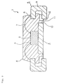
- Integrated circuit device 1 of an embodiment according to the present invention includes, as shown in Fig. 2, pellet 2 of an integrated circuit formed from a semiconductor circuit. This pellet 2 is mounted on an upper face of radiating plate 3 in the form of an island made of a metal.
- connection pads 4 are formed on an upper face of pellet 2.
- a large number of lead terminals 5 are arranged on the opposite sides of radiating plate 3.
- the large number of connection pads 4 of pellet 2 and inner portions 6 of the large number of lead terminals 5 are individually connected to each other by a large number of bonding wires 7.
- Pellet 2 part of radiating plate 3, bonding wires 7 and inner portions 6 of lead terminals 5 are encapsulated in resin package 8 which is a resin member.
- a large number of recesses 10 are formed on an outer peripheral portion of radiating plate 3.
- a large number of projections 11 are provided projectingly on an outer peripheral portion of the lower face of resin package 8. Those projections 11 are individually positioned in recesses 10 of radiating plate 3.
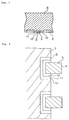
- recesses 12 each opened on the lower side and the outer side are formed on the bottom faces of large number of projections 11 of resin package 8. As shown in Figs. 3 and 4, the free ends of the large number of outer portions 9 of lead terminals 5 are individually positioned in recesses 12.
- each of projections 11 of resin package 8 is positioned in one of recesses 10 of radiating plate 3, and each of recesses 12 is formed on the lower face of one of projections 11 while the free end of outer portion 9 of each of lead terminals 5 is positioned in one of recesses 12.
- Integrated circuit device 1 of the present embodiment having the construction described above is mounted on an upper face of circuit board 13 as shown in Fig. 6d.
- the free ends of the large number of lead terminals 5 positioned on the lower face of resin package 8 are individually connected to a large number of signal lines 14 of circuit board 13 by solder 15, and radiating plate 3 exposed to the lower face of resin package 8 is connected to a conductor pattern such as grounding line 16 of circuit board 13 by solder 15.
- Integrated circuit device 1 mounted on circuit board 13 in this manner has a reduced mounting area since the outer portions of lead terminals 5 extending outwardly from the side faces of resin package 8 are bent in a J-shape such that the free ends thereof are positioned on the lower face of resin package 8.
- radiating plate 3 on which pellet 2 is mounted is exposed to the lower face of resin package 8 and is connected directly to grounding line 16, it can radiate heat of pellet 2 efficiently.
- the free ends of lead terminals 5 are positioned in recesses 10 formed on the outer peripheral portion of radiating plate 3. Since projections 11 of resin package 8 are positioned in the gaps between the free ends of lead terminals 5 and radiating plate 3 and serve as insulating members, lead terminals 5 and radiating plate 3 are not short-circuited to each other.
- radiating plate 3 is formed with a large area and realizes a good heat radiating property.
- a lead frame wherein a large number of lead terminals 5 and a single radiating plate 3 are integrally connected to each other by tie bars and so forth is formed by etching a very thin metal plate.
- radiating plate 3 is formed in such a shape that the large number of recesses 10 are positioned on an outer peripheral portion thereof.
- the lead frame is deformed by a press machine so that inner portions 6 of lead terminals 5 may be positioned higher than radiating plate 3, and pellet 2 is mounted onto the upper face of radiating plate 3 by solder.
- the large number of connection pads 4 of pellet 2 and the large number of lead terminals 5 are individually connected to each other by bonding wires 7.
- the lead frame on which pellet 2 and bonding wires 7 are mounted integrally in this manner is placed into a cavity of a pair of mutually removable metal molds.
- outer portions 9 of lead terminals 5 are held by and between the pair of metal molds and the lower face of radiating plate come into contact with the inner face of the metal molds so that those portions may be exposed from resin package 8.
- the metal molds used for molding of resin package 8 are formed in such a shape that projections 11 having recesses 12 formed on the lower faces thereof may be molded in recesses 10 of radiating plate 3.
- outer portions 9 of lead terminals 5 are bent at positions adjacent the free ends thereof by press metal dies 17 and 18, and outer portions 9 of lead terminals 5 are bent at positions adjacent the base ends thereof by press metal dies 19 and 20 as seen in Figs. 5b to 5e.
- lead terminals 5 are bent in a J-shape until the free ends thereof are moved to the lower face of resin package 8 and positioned in recesses 10 of radiating plate 3 with projections 11 of resin package 8 interposed therebetween.
- signal lines 14 and grounding line 16 are formed at positions of the upper face of circuit board 13 which correspond to radiating plate 3 and lead terminals 5 of integrated circuit device 1 as shown in Fig. 6a.
- solder 15 in the form of cream is applied to the surfaces of signal lines 14 and grounding line 16 and then integrated circuit device 1 is mounted onto the surface of signal lines 14 and grounding line 16 as seen in Figs. 6b and 6c, and then solder 15 is heated so as to be melted and then cooled so as to be solidified as seen in Fig. 6d.
- lead terminals 5 of integrated circuit device 1 are connected to signal lines 14 of circuit board 13 and radiating plate 3 is connected to grounding line 16. Accordingly, various signals can be inputted to and outputted from pellet 2, and pellet 2 can radiate heat efficiently.
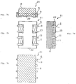
- lead terminals 5 and recesses 10 of radiating plate 3 correspond in a one-by-one corresponding relationship to each other.
- a plurality of lead terminals 5 may be positioned in each of recesses 23 of radiating plate 22.
- the area of radiating plate 22 is reduced and the heat radiating property is reduced a little.
- the productivity is augmented.
- radiating plate 32 may be formed in a simple rectangular shape with lead terminals 5 positioned on the opposite sides thereof such that the opposite portions of radiating plate 32 may serve as recesses 33.
- the area of radiating plate 32 is further reduced.
- the shape of radiating plate 32 is much simplified.
Abstract
Description
Claims (7)
- A semiconductor device comprising:a resin member having at least one recess formed on an outer peripheral portion of a lower face thereof;a pellet comprising a semiconductor circuit having a plurality of connection pads provided thereon and encapsulated in said resin member;a radiating plate having at least one recess formed on an outer peripheral portion thereof and having said pellet mounted on an upper face thereof and encapsulated in said resin member in such a condition as to be exposed to the lower face of said resin member;a plurality of lead terminals having inner portions encapsulated in said resin member and positioned on the outer sides of said pellet and outer portions extending outwardly from side faces of said resin member and bent in a J-shape such that free ends of said outer portions bent in a J-shape are positioned in said recess of the lower face of said resin member;a plurality of bonding wires encapsulated in said resin member for connecting said plurality of lead terminals and a plurality of connection pads of said pellet individually to each other; andinsulating element positioned in gaps between the free ends of said outer portions of said lead terminals and recess of said radiating plate.
- A semiconductor device, comprising:a pellet comprising a semiconductor circuit having a plurality of connection pads provided thereon;a radiating plate having at least one recess formed on an outer peripheral portion thereof and having said pellet mounted on an upper face thereof;a resin member having said pellet encapsulated therein and having said radiating plate encapsulated therein in such a manner as to be exposed to a lower face thereof, said resin member having at least one projection formed on an outer peripheral portion of the lower face thereof, said projection being positioned in said recess of said radiating plate, said resin member having at least one recess formed on lower faces of said projections thereof;a plurality of lead terminals having inner portions encapsulated in said resin member and positioned on the outer sides of said pellet and outer portions extending outwardly from side faces of said resin member and bent in a J-shape such that free ends of said outer portions bent in a J-shape are positioned in said recess of the lower faces of said projections of said resin member; anda plurality of bonding wires encapsulated in said resin member for connecting said plurality of lead terminals and said plurality of connection pads of said pellet individually to each other.
- A semiconductor device as claimed in claim 1, wherein the free end of the outer portion of each of said lead terminals is positioned in the recess of said radiating plate.
- A semiconductor device as claimed in claim 2, wherein the free end of the outer portion of each of said lead terminals is positioned in the recess of said radiating plate.
- A semiconductor device as claimed in claim 1, wherein the free ends of the outer portions of said plurality of lead terminals are positioned in the recess of said radiating plate.
- A semiconductor device as claimed in claim 2, wherein the free ends of the outer portions of said plurality of lead terminals are positioned in the recess of said radiating plate.
- A method of manufacturing a semiconductor device, comprising the steps of:forming a single lead frame wherein a single radiating plate having at least one recess formed on an outer peripheral portion thereof and a plurality of lead terminals are connected integrally to each other by support elements;placing a pellet of a semiconductor circuit having a plurality of connection pads provided on a surface thereof onto an upper face of a portion of the lead frame corresponding to the radiating plate;connecting the plurality of connection pads of the pellet and the plurality number of lead terminals of the lead frame individually to each other by bonding wires;placing the lead frame, on which the pellet and the bonding wires are mounted integrally, into a cavity of at least one pair of mutually removable metal molds such that a lower face of the radiating plate come into contact with an inner face of the metal molds and outer portions of the lead terminals are held by and between the pair of metal molds;filling a molten resin into the cavity of the metal molds;leaving the filled resin so as to be solidified to form a resin member wherein the pellet, at least a portion of the radiating plate, the bonding wires and inner portions of the lead terminals are encapsulated while outer portions of the lead terminals are exposed outside and at least one projection having at least one recess formed on lower faces thereof are formed in the recess of the radiating plate;cutting away the support elements of the lead frame to separate the radiating plate and the plurality of lead terminals individually from one another; andbending the outer portions of the lead terminals, which extend outwardly from side faces of the resin member, into a J-shape until free ends thereof are positioned in the recess of the outer peripheral portion of the lower face of the resin member.
Applications Claiming Priority (2)
| Application Number | Priority Date | Filing Date | Title |
|---|---|---|---|
| JP129671/97 | 1997-05-20 | ||
| JP9129671A JP2924854B2 (en) | 1997-05-20 | 1997-05-20 | Semiconductor device and manufacturing method thereof |
Publications (3)
| Publication Number | Publication Date |
|---|---|
| EP0880177A2 true EP0880177A2 (en) | 1998-11-25 |
| EP0880177A3 EP0880177A3 (en) | 1999-02-03 |
| EP0880177B1 EP0880177B1 (en) | 2007-08-29 |
Family
ID=15015285
Family Applications (1)
| Application Number | Title | Priority Date | Filing Date |
|---|---|---|---|
| EP98109023A Expired - Lifetime EP0880177B1 (en) | 1997-05-20 | 1998-05-18 | Semiconductor device having lead terminals bent in J-shape |
Country Status (7)
| Country | Link |
|---|---|
| US (2) | US6104086A (en) |
| EP (1) | EP0880177B1 (en) |
| JP (1) | JP2924854B2 (en) |
| KR (1) | KR100287236B1 (en) |
| CN (1) | CN1146044C (en) |
| DE (1) | DE69838310T2 (en) |
| TW (1) | TW494558B (en) |
Families Citing this family (63)
| Publication number | Priority date | Publication date | Assignee | Title |
|---|---|---|---|---|
| JP3842444B2 (en) * | 1998-07-24 | 2006-11-08 | 富士通株式会社 | Manufacturing method of semiconductor device |
| JP3839178B2 (en) * | 1999-01-29 | 2006-11-01 | 株式会社ルネサステクノロジ | Semiconductor device |
| JP3062192B1 (en) * | 1999-09-01 | 2000-07-10 | 松下電子工業株式会社 | Lead frame and method of manufacturing resin-encapsulated semiconductor device using the same |
| JP4395986B2 (en) * | 2000-04-24 | 2010-01-13 | 住友金属鉱山株式会社 | BCC lead frame, manufacturing method thereof, and semiconductor device obtained using the same |
| US7015072B2 (en) | 2001-07-11 | 2006-03-21 | Asat Limited | Method of manufacturing an enhanced thermal dissipation integrated circuit package |
| US6734552B2 (en) * | 2001-07-11 | 2004-05-11 | Asat Limited | Enhanced thermal dissipation integrated circuit package |
| US6790710B2 (en) * | 2002-01-31 | 2004-09-14 | Asat Limited | Method of manufacturing an integrated circuit package |
| US20030178719A1 (en) * | 2002-03-22 | 2003-09-25 | Combs Edward G. | Enhanced thermal dissipation integrated circuit package and method of manufacturing enhanced thermal dissipation integrated circuit package |
| US6940154B2 (en) * | 2002-06-24 | 2005-09-06 | Asat Limited | Integrated circuit package and method of manufacturing the integrated circuit package |
| US6897486B2 (en) * | 2002-12-06 | 2005-05-24 | Ban P. Loh | LED package die having a small footprint |
| SG143932A1 (en) * | 2003-05-30 | 2008-07-29 | Micron Technology Inc | Packaged microelectronic devices and methods of packaging microelectronic devices |
| US6934065B2 (en) * | 2003-09-18 | 2005-08-23 | Micron Technology, Inc. | Microelectronic devices and methods for packaging microelectronic devices |
| JP4372508B2 (en) * | 2003-10-06 | 2009-11-25 | ローム株式会社 | Lead frame manufacturing method, semiconductor device manufacturing method using the same, semiconductor device, and portable device and electronic device including the same |
| US7583862B2 (en) * | 2003-11-26 | 2009-09-01 | Aptina Imaging Corporation | Packaged microelectronic imagers and methods of packaging microelectronic imagers |
| US7253397B2 (en) * | 2004-02-23 | 2007-08-07 | Micron Technology, Inc. | Packaged microelectronic imagers and methods of packaging microelectronic imagers |
| US8092734B2 (en) * | 2004-05-13 | 2012-01-10 | Aptina Imaging Corporation | Covers for microelectronic imagers and methods for wafer-level packaging of microelectronics imagers |
| US7253957B2 (en) * | 2004-05-13 | 2007-08-07 | Micron Technology, Inc. | Integrated optics units and methods of manufacturing integrated optics units for use with microelectronic imagers |
| US20050275750A1 (en) * | 2004-06-09 | 2005-12-15 | Salman Akram | Wafer-level packaged microelectronic imagers and processes for wafer-level packaging |
| US7498647B2 (en) * | 2004-06-10 | 2009-03-03 | Micron Technology, Inc. | Packaged microelectronic imagers and methods of packaging microelectronic imagers |
| US7199439B2 (en) * | 2004-06-14 | 2007-04-03 | Micron Technology, Inc. | Microelectronic imagers and methods of packaging microelectronic imagers |
| US7262405B2 (en) * | 2004-06-14 | 2007-08-28 | Micron Technology, Inc. | Prefabricated housings for microelectronic imagers |
| US7232754B2 (en) | 2004-06-29 | 2007-06-19 | Micron Technology, Inc. | Microelectronic devices and methods for forming interconnects in microelectronic devices |
| US7294897B2 (en) * | 2004-06-29 | 2007-11-13 | Micron Technology, Inc. | Packaged microelectronic imagers and methods of packaging microelectronic imagers |
| US7416913B2 (en) * | 2004-07-16 | 2008-08-26 | Micron Technology, Inc. | Methods of manufacturing microelectronic imaging units with discrete standoffs |
| US7189954B2 (en) * | 2004-07-19 | 2007-03-13 | Micron Technology, Inc. | Microelectronic imagers with optical devices and methods of manufacturing such microelectronic imagers |
| US7402453B2 (en) * | 2004-07-28 | 2008-07-22 | Micron Technology, Inc. | Microelectronic imaging units and methods of manufacturing microelectronic imaging units |
| US20060023107A1 (en) * | 2004-08-02 | 2006-02-02 | Bolken Todd O | Microelectronic imagers with optics supports having threadless interfaces and methods for manufacturing such microelectronic imagers |
| US7364934B2 (en) * | 2004-08-10 | 2008-04-29 | Micron Technology, Inc. | Microelectronic imaging units and methods of manufacturing microelectronic imaging units |
| US7223626B2 (en) * | 2004-08-19 | 2007-05-29 | Micron Technology, Inc. | Spacers for packaged microelectronic imagers and methods of making and using spacers for wafer-level packaging of imagers |
| US7397066B2 (en) * | 2004-08-19 | 2008-07-08 | Micron Technology, Inc. | Microelectronic imagers with curved image sensors and methods for manufacturing microelectronic imagers |
| US7115961B2 (en) * | 2004-08-24 | 2006-10-03 | Micron Technology, Inc. | Packaged microelectronic imaging devices and methods of packaging microelectronic imaging devices |
| US7429494B2 (en) | 2004-08-24 | 2008-09-30 | Micron Technology, Inc. | Microelectronic imagers with optical devices having integral reference features and methods for manufacturing such microelectronic imagers |
| US7425499B2 (en) | 2004-08-24 | 2008-09-16 | Micron Technology, Inc. | Methods for forming interconnects in vias and microelectronic workpieces including such interconnects |
| US7276393B2 (en) * | 2004-08-26 | 2007-10-02 | Micron Technology, Inc. | Microelectronic imaging units and methods of manufacturing microelectronic imaging units |
| US20070148807A1 (en) * | 2005-08-22 | 2007-06-28 | Salman Akram | Microelectronic imagers with integrated optical devices and methods for manufacturing such microelectronic imagers |
| US7511262B2 (en) * | 2004-08-30 | 2009-03-31 | Micron Technology, Inc. | Optical device and assembly for use with imaging dies, and wafer-label imager assembly |
| US7646075B2 (en) * | 2004-08-31 | 2010-01-12 | Micron Technology, Inc. | Microelectronic imagers having front side contacts |
| US7300857B2 (en) | 2004-09-02 | 2007-11-27 | Micron Technology, Inc. | Through-wafer interconnects for photoimager and memory wafers |
| KR100577430B1 (en) | 2004-09-03 | 2006-05-08 | 삼성전자주식회사 | Display apparatus |
| US7271482B2 (en) * | 2004-12-30 | 2007-09-18 | Micron Technology, Inc. | Methods for forming interconnects in microelectronic workpieces and microelectronic workpieces formed using such methods |
| US7214919B2 (en) * | 2005-02-08 | 2007-05-08 | Micron Technology, Inc. | Microelectronic imaging units and methods of manufacturing microelectronic imaging units |
| US20060177999A1 (en) * | 2005-02-10 | 2006-08-10 | Micron Technology, Inc. | Microelectronic workpieces and methods for forming interconnects in microelectronic workpieces |
| US7303931B2 (en) * | 2005-02-10 | 2007-12-04 | Micron Technology, Inc. | Microfeature workpieces having microlenses and methods of forming microlenses on microfeature workpieces |
| US8093694B2 (en) * | 2005-02-14 | 2012-01-10 | Stats Chippac Ltd. | Method of manufacturing non-leaded integrated circuit package system having etched differential height lead structures |
| US7190039B2 (en) * | 2005-02-18 | 2007-03-13 | Micron Technology, Inc. | Microelectronic imagers with shaped image sensors and methods for manufacturing microelectronic imagers |
| US20060290001A1 (en) * | 2005-06-28 | 2006-12-28 | Micron Technology, Inc. | Interconnect vias and associated methods of formation |
| US7795134B2 (en) | 2005-06-28 | 2010-09-14 | Micron Technology, Inc. | Conductive interconnect structures and formation methods using supercritical fluids |
| US7288757B2 (en) * | 2005-09-01 | 2007-10-30 | Micron Technology, Inc. | Microelectronic imaging devices and associated methods for attaching transmissive elements |
| US7262134B2 (en) | 2005-09-01 | 2007-08-28 | Micron Technology, Inc. | Microfeature workpieces and methods for forming interconnects in microfeature workpieces |
| SG135979A1 (en) * | 2006-03-08 | 2007-10-29 | Micron Technology Inc | Microelectronic device assemblies including assemblies with recurved leadframes, and associated methods |
| SG139573A1 (en) * | 2006-07-17 | 2008-02-29 | Micron Technology Inc | Microelectronic packages with leadframes, including leadframes configured for stacked die packages, and associated systems and methods |
| JP5028968B2 (en) * | 2006-11-17 | 2012-09-19 | 日立電線株式会社 | Semiconductor device, stacked semiconductor device, and interposer substrate |
| US8035207B2 (en) * | 2006-12-30 | 2011-10-11 | Stats Chippac Ltd. | Stackable integrated circuit package system with recess |
| SG149726A1 (en) | 2007-07-24 | 2009-02-27 | Micron Technology Inc | Microelectronic die packages with metal leads, including metal leads for stacked die packages, and associated systems and methods |
| SG150396A1 (en) * | 2007-08-16 | 2009-03-30 | Micron Technology Inc | Microelectronic die packages with leadframes, including leadframe-based interposer for stacked die packages, and associated systems and methods |
| US20100194465A1 (en) * | 2009-02-02 | 2010-08-05 | Ali Salih | Temperature compensated current source and method therefor |
| JP2011103286A (en) * | 2009-10-15 | 2011-05-26 | Panasonic Corp | Push-on switch |
| CN102223753B (en) * | 2010-04-16 | 2013-08-28 | 富葵精密组件(深圳)有限公司 | Circuit board and production method thereof |
| JP5876669B2 (en) * | 2010-08-09 | 2016-03-02 | ルネサスエレクトロニクス株式会社 | Semiconductor device |
| JP4996729B2 (en) * | 2010-09-15 | 2012-08-08 | 株式会社東芝 | Electronics and board assembly |
| CN102842786A (en) * | 2011-06-22 | 2012-12-26 | 苏州快可光伏电子股份有限公司 | Terminal set of connection box |
| CN105206596B (en) | 2014-06-06 | 2018-12-07 | 恩智浦美国有限公司 | Packaging integrated circuit devices with bending lead |
| JP2020047771A (en) * | 2018-09-19 | 2020-03-26 | Tdk株式会社 | Terminal bending apparatus, terminal bending method, and method of manufacturing coil component |
Citations (3)
| Publication number | Priority date | Publication date | Assignee | Title |
|---|---|---|---|---|
| US3930114A (en) * | 1975-03-17 | 1975-12-30 | Nat Semiconductor Corp | Integrated circuit package utilizing novel heat sink structure |
| GB2154791A (en) * | 1984-02-17 | 1985-09-11 | Ates Componenti Elettron | Packaging semiconductor devices |
| US4698660A (en) * | 1982-03-30 | 1987-10-06 | Fujitsu Limited | Resin-molded semiconductor device |
Family Cites Families (14)
| Publication number | Priority date | Publication date | Assignee | Title |
|---|---|---|---|---|
| US4496965A (en) * | 1981-05-18 | 1985-01-29 | Texas Instruments Incorporated | Stacked interdigitated lead frame assembly |
| US5287000A (en) | 1987-10-20 | 1994-02-15 | Hitachi, Ltd. | Resin-encapsulated semiconductor memory device useful for single in-line packages |
| US5266834A (en) * | 1989-03-13 | 1993-11-30 | Hitachi Ltd. | Semiconductor device and an electronic device with the semiconductor devices mounted thereon |
| JP2799408B2 (en) * | 1989-12-22 | 1998-09-17 | 株式会社日立製作所 | Semiconductor device and electronic device mounting the same |
| US5148265A (en) | 1990-09-24 | 1992-09-15 | Ist Associates, Inc. | Semiconductor chip assemblies with fan-in leads |
| US5375320A (en) | 1991-08-13 | 1994-12-27 | Micron Technology, Inc. | Method of forming "J" leads on a semiconductor device |
| JP2682936B2 (en) | 1992-02-07 | 1997-11-26 | ローム株式会社 | Semiconductor device |
| JPH0661408A (en) * | 1992-08-10 | 1994-03-04 | Rohm Co Ltd | Surface mount type semiconductor device |
| US5406117A (en) * | 1993-12-09 | 1995-04-11 | Dlugokecki; Joseph J. | Radiation shielding for integrated circuit devices using reconstructed plastic packages |
| JP2713141B2 (en) * | 1994-02-02 | 1998-02-16 | 日本電気株式会社 | Semiconductor device |
| JPH07263607A (en) * | 1994-03-17 | 1995-10-13 | Sumitomo Kinzoku Ceramics:Kk | Semiconductor package with j-lead and bending method of lead frame |
| JPH0883870A (en) * | 1994-09-12 | 1996-03-26 | Ricoh Co Ltd | Resin sealed semiconductor device |
| JPH0888296A (en) * | 1994-09-20 | 1996-04-02 | Fujitsu Ltd | Semiconductor device, manufacture thereof and semiconductor device unit |
| JPH09260568A (en) * | 1996-03-27 | 1997-10-03 | Mitsubishi Electric Corp | Semiconductor device and its manufacture |
-
1997
- 1997-05-20 JP JP9129671A patent/JP2924854B2/en not_active Expired - Fee Related
-
1998
- 1998-04-13 TW TW087105687A patent/TW494558B/en not_active IP Right Cessation
- 1998-04-13 US US09/059,316 patent/US6104086A/en not_active Expired - Lifetime
- 1998-05-12 CN CNB981018467A patent/CN1146044C/en not_active Expired - Fee Related
- 1998-05-18 KR KR1019980017825A patent/KR100287236B1/en not_active IP Right Cessation
- 1998-05-18 DE DE69838310T patent/DE69838310T2/en not_active Expired - Fee Related
- 1998-05-18 EP EP98109023A patent/EP0880177B1/en not_active Expired - Lifetime
-
1999
- 1999-10-14 US US09/417,745 patent/US6319753B1/en not_active Expired - Lifetime
Patent Citations (3)
| Publication number | Priority date | Publication date | Assignee | Title |
|---|---|---|---|---|
| US3930114A (en) * | 1975-03-17 | 1975-12-30 | Nat Semiconductor Corp | Integrated circuit package utilizing novel heat sink structure |
| US4698660A (en) * | 1982-03-30 | 1987-10-06 | Fujitsu Limited | Resin-molded semiconductor device |
| GB2154791A (en) * | 1984-02-17 | 1985-09-11 | Ates Componenti Elettron | Packaging semiconductor devices |
Non-Patent Citations (2)
| Title |
|---|
| PATENT ABSTRACTS OF JAPAN vol. 018, no. 299 (E-1558), 8 June 1994 & JP 06 061408 A (ROHM CO LTD), 4 March 1994 * |
| PATENT ABSTRACTS OF JAPAN vol. 096, no. 007, 31 July 1996 & JP 08 083870 A (RICOH CO LTD), 26 March 1996 * |
Also Published As
| Publication number | Publication date |
|---|---|
| EP0880177A3 (en) | 1999-02-03 |
| CN1146044C (en) | 2004-04-14 |
| JPH10321788A (en) | 1998-12-04 |
| DE69838310T2 (en) | 2008-05-15 |
| CN1202009A (en) | 1998-12-16 |
| JP2924854B2 (en) | 1999-07-26 |
| US6104086A (en) | 2000-08-15 |
| TW494558B (en) | 2002-07-11 |
| DE69838310D1 (en) | 2007-10-11 |
| KR100287236B1 (en) | 2001-11-22 |
| EP0880177B1 (en) | 2007-08-29 |
| US6319753B1 (en) | 2001-11-20 |
| KR19980087150A (en) | 1998-12-05 |
Similar Documents
| Publication | Publication Date | Title |
|---|---|---|
| US6104086A (en) | Semiconductor device having lead terminals bent in J-shape | |
| EP1662565B1 (en) | Semiconductor package | |
| US6630729B2 (en) | Low-profile semiconductor package with strengthening structure | |
| JP3027954B2 (en) | Integrated circuit device and manufacturing method thereof | |
| EP0880176B1 (en) | Semiconductor device having pellet mounted on radiating plate thereof | |
| KR20050039833A (en) | Substrate based unmolded package | |
| US6780679B2 (en) | Semiconductor device and method of manufacturing the same | |
| KR100286906B1 (en) | Method for manufacturing a semiconductor device having a pair of heat dissipation terminals and a plurality of lead terminals formed from a single lead frame, and a single lead frame | |
| JP3003638B2 (en) | Semiconductor device and manufacturing method thereof | |
| JP3061120B2 (en) | Semiconductor device and manufacturing method thereof | |
| JP3730469B2 (en) | Resin-sealed semiconductor device and manufacturing method thereof | |
| US6396132B1 (en) | Semiconductor device with improved interconnections between the chip and the terminals, and process for its manufacture | |
| JP3495566B2 (en) | Semiconductor device | |
| US20220110213A1 (en) | Mechanical support within moulded chip package | |
| JP3867881B2 (en) | Semiconductor device | |
| JPH08264705A (en) | Semiconductor device and package structure and packaging method using the same | |
| JPH1154682A (en) | Semiconductor device and its manufacture | |
| KR20010060872A (en) | Semiconductor chip package and manufacturing method thereof |
Legal Events
| Date | Code | Title | Description |
|---|---|---|---|
| PUAI | Public reference made under article 153(3) epc to a published international application that has entered the european phase |
Free format text: ORIGINAL CODE: 0009012 |
|
| AK | Designated contracting states |
Kind code of ref document: A2 Designated state(s): DE FR GB |
|
| AX | Request for extension of the european patent |
Free format text: AL;LT;LV;MK;RO;SI |
|
| PUAL | Search report despatched |
Free format text: ORIGINAL CODE: 0009013 |
|
| AK | Designated contracting states |
Kind code of ref document: A3 Designated state(s): AT BE CH CY DE DK ES FI FR GB GR IE IT LI LU MC NL PT SE |
|
| AX | Request for extension of the european patent |
Free format text: AL;LT;LV;MK;RO;SI |
|
| 17P | Request for examination filed |
Effective date: 19990309 |
|
| AKX | Designation fees paid |
Free format text: DE FR GB |
|
| RAP1 | Party data changed (applicant data changed or rights of an application transferred) |
Owner name: NEC COMPOUND SEMICONDUCTOR DEVICES, LTD. |
|
| RAP1 | Party data changed (applicant data changed or rights of an application transferred) |
Owner name: NEC ELECTRONICS CORPORATION |
|
| 17Q | First examination report despatched |
Effective date: 20060623 |
|
| GRAP | Despatch of communication of intention to grant a patent |
Free format text: ORIGINAL CODE: EPIDOSNIGR1 |
|
| RIC1 | Information provided on ipc code assigned before grant |
Ipc: H01L 23/31 20060101ALI20070314BHEP Ipc: H01L 21/48 20060101ALI20070314BHEP Ipc: H01L 23/433 20060101ALI20070314BHEP Ipc: H01L 23/495 20060101ALI20070314BHEP Ipc: H01L 23/36 20060101AFI20070314BHEP |
|
| GRAS | Grant fee paid |
Free format text: ORIGINAL CODE: EPIDOSNIGR3 |
|
| GRAA | (expected) grant |
Free format text: ORIGINAL CODE: 0009210 |
|
| AK | Designated contracting states |
Kind code of ref document: B1 Designated state(s): DE FR GB |
|
| REG | Reference to a national code |
Ref country code: GB Ref legal event code: FG4D |
|
| REF | Corresponds to: |
Ref document number: 69838310 Country of ref document: DE Date of ref document: 20071011 Kind code of ref document: P |
|
| ET | Fr: translation filed | ||
| PLBE | No opposition filed within time limit |
Free format text: ORIGINAL CODE: 0009261 |
|
| STAA | Information on the status of an ep patent application or granted ep patent |
Free format text: STATUS: NO OPPOSITION FILED WITHIN TIME LIMIT |
|
| 26N | No opposition filed |
Effective date: 20080530 |
|
| PGFP | Annual fee paid to national office [announced via postgrant information from national office to epo] |
Ref country code: FR Payment date: 20090515 Year of fee payment: 12 Ref country code: DE Payment date: 20090514 Year of fee payment: 12 |
|
| PGFP | Annual fee paid to national office [announced via postgrant information from national office to epo] |
Ref country code: GB Payment date: 20090513 Year of fee payment: 12 |
|
| GBPC | Gb: european patent ceased through non-payment of renewal fee |
Effective date: 20100518 |
|
| REG | Reference to a national code |
Ref country code: FR Ref legal event code: ST Effective date: 20110131 |
|
| PG25 | Lapsed in a contracting state [announced via postgrant information from national office to epo] |
Ref country code: DE Free format text: LAPSE BECAUSE OF NON-PAYMENT OF DUE FEES Effective date: 20101201 |
|
| PG25 | Lapsed in a contracting state [announced via postgrant information from national office to epo] |
Ref country code: FR Free format text: LAPSE BECAUSE OF NON-PAYMENT OF DUE FEES Effective date: 20100531 |
|
| PG25 | Lapsed in a contracting state [announced via postgrant information from national office to epo] |
Ref country code: GB Free format text: LAPSE BECAUSE OF NON-PAYMENT OF DUE FEES Effective date: 20100518 |