EP0878355A2 - Verfahren und Vorrichtung zur Flüssigkeitverteilung auf einem unebenen Substrat - Google Patents
Verfahren und Vorrichtung zur Flüssigkeitverteilung auf einem unebenen Substrat Download PDFInfo
- Publication number
- EP0878355A2 EP0878355A2 EP98303300A EP98303300A EP0878355A2 EP 0878355 A2 EP0878355 A2 EP 0878355A2 EP 98303300 A EP98303300 A EP 98303300A EP 98303300 A EP98303300 A EP 98303300A EP 0878355 A2 EP0878355 A2 EP 0878355A2
- Authority
- EP
- European Patent Office
- Prior art keywords
- base
- pins
- substrate
- solder
- array
- Prior art date
- Legal status (The legal status is an assumption and is not a legal conclusion. Google has not performed a legal analysis and makes no representation as to the accuracy of the status listed.)
- Withdrawn
Links
Images


Classifications
-
- H—ELECTRICITY
- H05—ELECTRIC TECHNIQUES NOT OTHERWISE PROVIDED FOR
- H05K—PRINTED CIRCUITS; CASINGS OR CONSTRUCTIONAL DETAILS OF ELECTRIC APPARATUS; MANUFACTURE OF ASSEMBLAGES OF ELECTRICAL COMPONENTS
- H05K3/00—Apparatus or processes for manufacturing printed circuits
- H05K3/30—Assembling printed circuits with electric components, e.g. with resistors
- H05K3/32—Assembling printed circuits with electric components, e.g. with resistors electrically connecting electric components or wires to printed circuits
- H05K3/34—Assembling printed circuits with electric components, e.g. with resistors electrically connecting electric components or wires to printed circuits by soldering
- H05K3/3465—Application of solder
- H05K3/3485—Application of solder paste, slurry or powder
-
- H—ELECTRICITY
- H02—GENERATION; CONVERSION OR DISTRIBUTION OF ELECTRIC POWER
- H02G—INSTALLATION OF ELECTRIC CABLES OR LINES, OR OF COMBINED OPTICAL AND ELECTRIC CABLES OR LINES
- H02G3/00—Installations of electric cables or lines or protective tubing therefor in or on buildings, equivalent structures or vehicles
- H02G3/26—Installations of cables, lines, or separate protective tubing therefor directly on or in walls, ceilings, or floors
- H02G3/266—Mounting by adhesive material
-
- H—ELECTRICITY
- H05—ELECTRIC TECHNIQUES NOT OTHERWISE PROVIDED FOR
- H05K—PRINTED CIRCUITS; CASINGS OR CONSTRUCTIONAL DETAILS OF ELECTRIC APPARATUS; MANUFACTURE OF ASSEMBLAGES OF ELECTRICAL COMPONENTS
- H05K1/00—Printed circuits
- H05K1/02—Details
- H05K1/0284—Details of three-dimensional rigid printed circuit boards
-
- H—ELECTRICITY
- H05—ELECTRIC TECHNIQUES NOT OTHERWISE PROVIDED FOR
- H05K—PRINTED CIRCUITS; CASINGS OR CONSTRUCTIONAL DETAILS OF ELECTRIC APPARATUS; MANUFACTURE OF ASSEMBLAGES OF ELECTRICAL COMPONENTS
- H05K2201/00—Indexing scheme relating to printed circuits covered by H05K1/00
- H05K2201/09—Shape and layout
- H05K2201/09009—Substrate related
- H05K2201/09018—Rigid curved substrate
-
- H—ELECTRICITY
- H05—ELECTRIC TECHNIQUES NOT OTHERWISE PROVIDED FOR
- H05K—PRINTED CIRCUITS; CASINGS OR CONSTRUCTIONAL DETAILS OF ELECTRIC APPARATUS; MANUFACTURE OF ASSEMBLAGES OF ELECTRICAL COMPONENTS
- H05K2203/00—Indexing scheme relating to apparatus or processes for manufacturing printed circuits covered by H05K3/00
- H05K2203/01—Tools for processing; Objects used during processing
- H05K2203/0195—Tool for a process not provided for in H05K3/00, e.g. tool for handling objects using suction, for deforming objects, for applying local pressure
-
- H—ELECTRICITY
- H05—ELECTRIC TECHNIQUES NOT OTHERWISE PROVIDED FOR
- H05K—PRINTED CIRCUITS; CASINGS OR CONSTRUCTIONAL DETAILS OF ELECTRIC APPARATUS; MANUFACTURE OF ASSEMBLAGES OF ELECTRICAL COMPONENTS
- H05K2203/00—Indexing scheme relating to apparatus or processes for manufacturing printed circuits covered by H05K3/00
- H05K2203/03—Metal processing
- H05K2203/0338—Transferring metal or conductive material other than a circuit pattern, e.g. bump, solder, printed component
-
- H—ELECTRICITY
- H05—ELECTRIC TECHNIQUES NOT OTHERWISE PROVIDED FOR
- H05K—PRINTED CIRCUITS; CASINGS OR CONSTRUCTIONAL DETAILS OF ELECTRIC APPARATUS; MANUFACTURE OF ASSEMBLAGES OF ELECTRICAL COMPONENTS
- H05K3/00—Apparatus or processes for manufacturing printed circuits
- H05K3/30—Assembling printed circuits with electric components, e.g. with resistors
- H05K3/32—Assembling printed circuits with electric components, e.g. with resistors electrically connecting electric components or wires to printed circuits
- H05K3/34—Assembling printed circuits with electric components, e.g. with resistors electrically connecting electric components or wires to printed circuits by soldering
- H05K3/3465—Application of solder
- H05K3/3478—Application of solder preforms; Transferring prefabricated solder patterns
Definitions
- the present invention relates to a fluid dispensing method and apparatus, and more particularly to a method and apparatus for dispensing solder paste, adhesive, or other liquid or paste-like material at a plurality of locations on a non-planar substrate.
- circuit patterns directly onto vehicle structural components are typically three-dimensional or non-planar, therefore the circuit pattern must be applied onto the non-planar surface. Accordingly, dispensing solder paste onto discrete locations on the circuit pattern to form electrically conductive solder joints once the circuit pattern has been applied to the non-planar surface is problematic because efficient technology does not exist for applying solder at a plurality of discrete locations on a non-planar surface.
- solder paste and other fluids such as glue
- the present invention provides a fluid transfer device which includes a movable base and an array of pins extending from the base, wherein each pin includes a distal end which is movable with respect to the base independently of the rest of the array of pins, such that the distal ends of the pins may transfer fluid to discrete locations on a non-planar surface.
- the present invention provides an apparatus for applying fluid to a plurality of locations on a non-planar substrate, including a movable base and an array of pins connected to the base.
- Each pin has a distal end which is vertically movable with respect to the base independently of the rest of the array of pins, wherein each distal end is adapted to transfer fluid to a location on the non-planar substrate.
- the distal ends of the pins have a greater affinity for the fluid than the fluid has for itself and a lesser affinity for the fluid than the fluid has for the substrate.
- the distal ends may be dipped in the fluid and moved into contact with the substrate such that individual distal ends may collapse toward the base as the distal ends engage the substrate to facilitate further movement of the base toward the substrate for application of fluid to each of the plurality of locations.
- the fluid may be a solder, glue, etc.
- the present invention further provides a method of applying solder to a plurality of locations on a non-planar electronic substrate, comprising: 1) providing a solder transfer device including a movable base with an array of pins connected to the base, each pin having a distal end which is vertically movable with respect to the base independently of the rest of the array of pins; 2) dipping the distal ends of the pins in a tray of solder paste; and 3) moving the base toward the non-planar electronic substrate such that the distal ends of the array of pins contact the plurality of locations for applying the solder paste to the locations.
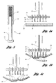
- Figures 1a-1f schematically illustrate a sequence of transferring solder paste to a solder pad on a substrate.
- a pin 10 with a distal end portion 12 is moved toward and dipped in a tray of solder paste 14 in Figures 1a and 1b, and withdrawn from the solder paste with a droplet of solder 16 remaining on the distal end 12 of the pin 10, as shown in Figure 1c.
- the pin 10 is then positioned over a substrate 18 with a solder pad 20 thereon, as shown in Figure 1d.
- the distal end 12 of the pin 10 is then brought into contact with the pad 20, and removed from the pad 20 to leave the solder paste droplet 16 on the pad 20, as shown in Figures 1e and 1f.
- the apparatus 24 for applying solder to a plurality of locations on a non-planar substrate 26 includes a movable base 28 with an array of pins 30 slidably mounted for vertical movement with respect to the base 28. Each of the array of pins 30 includes a distal end 32 adapted for transferring solder paste to a solder location. As shown, the substrate 26 includes a non-planar surface 34. Because the pins 30 are allowed to float with respect to the base 28, the distal ends 32 of the pins 30 will conform with the contoured shape of the non-planar surface 34 of the substrate 26 for application of solder at discrete locations along the surface 34.
- the pins 30 could be moved merely by gravity, or they could be under computer control, and data could be transferred from CAD equipment to set the pin height according to the substrate surface 34.
- the pins 30 could then be pneumatically or electromechanically driven to the desired height for properly positioning the distal ends 30 of the pins for solder transfer.
- Figure 3 shows an alternative pin design 40 in which the pin assembly has a distal end portion 44 which is movable vertically with respect to the pin 42 by means of a compressible spring 46 which engages a shaft 48 for allowing such respective vertical movement.
- FIG. 4a-4c Implementation of the embodiment shown in Figure 3 is illustrated in Figures 4a-4c.
- a driver 52 is used for moving the movable base 54, which includes pins 42 connected thereto.
- each pin comprises a shaft 48 which is spring-loaded with respect to the pin 42, and a distal end portion 44 connected to the shaft 48.
- the distal ends 44 may comprise different geometries for transferring different amounts of paste.
- the distal ends 44 are dipped in the paste 56 in the tray 58.
- the driver 52 then pulls the base 54 and pins away from the tray 58 and positions the pins over the three-dimensional substrate 60 to which the paste will be applied.
- the driver 52 then moves the base 54 so that the distal ends 44 contact the substrate 60 for applying the paste to the substrate.
- the driver 52 then pulls the base 54 and pins away from the substrate 60, leaving the solder paste on the substrate 60.
- FIG. 5a-5d A second alternative embodiment of the invention is illustrated in Figures 5a-5d.
- the tray 70 is covered with a plate 72 having apertures 74, 76, 78 formed therethrough to allow only selected pins of the array of pins 80 to pass through the plate 72 to be dipped in the solder paste 82 (or adhesive, etc.).
- the relative affinity of the solder paste for the distal end of the pin is greater than the cohesive strength of the solder paste, which allows the distal ends of the pin to pick up droplets of solder paste. This is accomplished by surfactant and rheological modification of the paste along with specialised pin coatings.
- the affinity of the paste is also greater for the solder pad than it is for the pin, which allows efficient paste transfer during the process.
- the pins may be coated with some material like sintered Teflon, titanium nitride, or the surface may be hardened.
- the transfer pins may have a variety of distal end head designs.
- the distal ends of the pins may be straight, flared, pointed, fluted, serrated, etc.
- the distal ends could also be round or could include a ball joint configuration to allow slope conformance on angled surfaces.
- multiple pins may be used to transfer the desired amount of solder, and the pins may be spring-loaded or individually or group-actuated with a number of electronic or mechanical devices. Ultrasonic agitation may be used to provide efficient transfer of solder paste.
- the pins may also be hollow to provide for an array of syringes to provide a high volume of paste in a small area. Such an array of syringes could be pneumatically actuated, and the pin array could alternatively be heated or cooled to assist in solder paste transfer or to assist in the subsequent reflow process.
- the pins may also be heated to enable the transfer of molten solder droplets to the pad and/or components. This eliminates the high temperature solder reflow processing for temperature-sensitive substrates.
- the transfer pin array may be custom configured for the specific part on which solder paste is to be dispensed, or could be a generic array in which specific pins could be used for specific dispense situations. This attribute allows for rapid flexible manufacturing.
- This same basic apparatus may be used to rapidly dispense other electronic packaging materials in three dimensions, such as solder fluxes, conformal coatings, and surface mount device adhesives.
- Surface mount device adhesive attachment is useful, not only for bottom side component processing through a solder wave, but also for anchoring devices to flat and angled surfaces during handling prior to reflow.
Landscapes
- Engineering & Computer Science (AREA)
- Architecture (AREA)
- Civil Engineering (AREA)
- Structural Engineering (AREA)
- Manufacturing & Machinery (AREA)
- Microelectronics & Electronic Packaging (AREA)
- Electric Connection Of Electric Components To Printed Circuits (AREA)
- Coating Apparatus (AREA)
Applications Claiming Priority (2)
| Application Number | Priority Date | Filing Date | Title |
|---|---|---|---|
| US08/857,159 US5909839A (en) | 1997-05-15 | 1997-05-15 | Method for dispensing solder paste on a non-planar substrate using an array of ultrasonically agitated pins |
| US857159 | 1997-05-15 |
Publications (2)
| Publication Number | Publication Date |
|---|---|
| EP0878355A2 true EP0878355A2 (de) | 1998-11-18 |
| EP0878355A3 EP0878355A3 (de) | 2001-10-24 |
Family
ID=25325332
Family Applications (1)
| Application Number | Title | Priority Date | Filing Date |
|---|---|---|---|
| EP98303300A Withdrawn EP0878355A3 (de) | 1997-05-15 | 1998-04-28 | Verfahren und Vorrichtung zur Flüssigkeitverteilung auf einem unebenen Substrat |
Country Status (3)
| Country | Link |
|---|---|
| US (1) | US5909839A (de) |
| EP (1) | EP0878355A3 (de) |
| CA (1) | CA2232172A1 (de) |
Cited By (1)
| Publication number | Priority date | Publication date | Assignee | Title |
|---|---|---|---|---|
| FR2835204A1 (fr) * | 2002-01-25 | 2003-08-01 | Bosch Gmbh Robert | Outil pour appliquer ou imprimer une colle sur un substrat et procede de mise en oeuvre |
Families Citing this family (12)
| Publication number | Priority date | Publication date | Assignee | Title |
|---|---|---|---|---|
| US6059176A (en) * | 1997-04-11 | 2000-05-09 | Pac Tech Packaging Technologies G.M.B.H. | Device and a method for applying a plurality of solder globules to a substrate |
| US7142083B2 (en) | 2002-09-17 | 2006-11-28 | Lindsey Raymond A | Electronics component and method for fabricating same |
| DE102005060178B4 (de) * | 2005-12-14 | 2010-04-15 | Eads Deutschland Gmbh | Reibrühr-Werkzeug mit formanpassbarer Schulter und dessen Verwendung |
| KR100897132B1 (ko) | 2007-09-12 | 2009-05-14 | 삼성모바일디스플레이주식회사 | 표시패널 봉지장치 및 이를 이용한 유기전계발광표시장치의 제조방법 |
| US9162249B2 (en) * | 2008-10-01 | 2015-10-20 | Panasonic Intellectual Property Management Co., Ltd. | Paste dispenser for applying paste containing fillers using nozzle with pin and application method using the same |
| US8371497B2 (en) * | 2009-06-11 | 2013-02-12 | Qualcomm Incorporated | Method for manufacturing tight pitch, flip chip integrated circuit packages |
| US8534533B2 (en) * | 2012-01-19 | 2013-09-17 | Raytheon Company | Solder paste transfer process |
| US8770462B2 (en) * | 2012-03-14 | 2014-07-08 | Raytheon Company | Solder paste transfer process |
| US20140055961A1 (en) * | 2012-08-23 | 2014-02-27 | Shayan Malek | Printed Circuit Boards with Recesses |
| US9216469B2 (en) * | 2013-10-18 | 2015-12-22 | Taiwan Semiconductor Manufacturing Co., Ltd. | Indirect printing bumping method for solder ball deposition |
| DE102013112348B4 (de) * | 2013-11-11 | 2024-05-08 | Endress+Hauser SE+Co. KG | Lotauftragsstempel und Verfahren zur Reparatur einer Leiterplatte mit zumindest einem defekten Bauteil |
| DE102019118574A1 (de) * | 2019-07-09 | 2021-01-14 | Endress+Hauser SE+Co. KG | Stift zum Übertragen von Lotpaste aus einem Reservoir auf eine Kontaktstelle einer Leiterplatte |
Family Cites Families (8)
| Publication number | Priority date | Publication date | Assignee | Title |
|---|---|---|---|---|
| DE2935081C2 (de) * | 1979-08-30 | 1985-12-19 | Philips Patentverwaltung Gmbh, 2000 Hamburg | Vorrichtung zur Bestückung von Leiterplatten. |
| US4421266A (en) * | 1981-07-29 | 1983-12-20 | Western Electric Company, Inc. | Handling bodies containing bonding material |
| NL8304185A (nl) * | 1983-12-06 | 1985-07-01 | Philips Nv | Stempel en inrichting voor het aanbrengen van druppels van een viskeuze vloeistof op een substraat. |
| US4946708A (en) * | 1988-11-18 | 1990-08-07 | International Business Machines Corporation | Pin transfer adhesive application for surface mount component processes |
| US5186982A (en) * | 1990-09-18 | 1993-02-16 | Minnesota Mining And Manufacturing Company | Pin transfer applicator and method |
| JPH05175645A (ja) * | 1991-12-26 | 1993-07-13 | Toshiba Corp | 電子部品の半田付け装置 |
| US5435481A (en) * | 1994-01-18 | 1995-07-25 | Motorola, Inc. | Soldering process |
| US5676305A (en) * | 1996-04-18 | 1997-10-14 | Motorola, Inc. | Method to achieve regulated force contact in pin transfer deposition of liquidus substances |
-
1997
- 1997-05-15 US US08/857,159 patent/US5909839A/en not_active Expired - Fee Related
-
1998
- 1998-03-16 CA CA002232172A patent/CA2232172A1/en not_active Abandoned
- 1998-04-28 EP EP98303300A patent/EP0878355A3/de not_active Withdrawn
Cited By (1)
| Publication number | Priority date | Publication date | Assignee | Title |
|---|---|---|---|---|
| FR2835204A1 (fr) * | 2002-01-25 | 2003-08-01 | Bosch Gmbh Robert | Outil pour appliquer ou imprimer une colle sur un substrat et procede de mise en oeuvre |
Also Published As
| Publication number | Publication date |
|---|---|
| CA2232172A1 (en) | 1998-11-15 |
| EP0878355A3 (de) | 2001-10-24 |
| US5909839A (en) | 1999-06-08 |
Similar Documents
| Publication | Publication Date | Title |
|---|---|---|
| US5909839A (en) | Method for dispensing solder paste on a non-planar substrate using an array of ultrasonically agitated pins | |
| US4722470A (en) | Method and transfer plate for applying solder to component leads | |
| US5373984A (en) | Reflow process for mixed technology on a printed wiring board | |
| EP0582375A1 (de) | Aufbringen von Lotteilchen | |
| EP0565908B1 (de) | Verfahren zum Spritzgiessen von Lot und deren Anwendung | |
| US5834062A (en) | Material transfer apparatus and method of using the same | |
| US6193144B1 (en) | Paste providing method, soldering method and apparatus and system therefor | |
| CN115038591A (zh) | 以高分辨率印刷焊膏和其他粘性材料的系统与方法 | |
| US5676305A (en) | Method to achieve regulated force contact in pin transfer deposition of liquidus substances | |
| KR20220143025A (ko) | 땜납 페이스트를 부품에 인쇄하기 위한 시스템 및 방법 | |
| US5890283A (en) | Apparatus and method for mounting electrically conductive balls | |
| US10237982B2 (en) | Solder application stamp for applying solder on contact locations possessing small dimensions | |
| EP1314342B1 (de) | Verfahren, vorrichtung und verwendung des auftragens eines viskosen mediums auf ein substrat | |
| DE10105164A1 (de) | Verfahren und Vorrichtung zum Kontaktieren von Halbleiterchips | |
| JP7332720B2 (ja) | 部品実装機及び転写材転写方法 | |
| JPH0419908B2 (de) | ||
| EP2695506A1 (de) | Verfahren und flüssigkeitsübertragungseinheit mit quetschwalzen zur bereitstellung einer glatten flüssigkeitsoberfläche | |
| MXPA98002053A (en) | Method and apparatus to distribute fluid on a substrate no pl | |
| Feldmann et al. | Analytical and experimental research on assembly systems for molded interconnection devices (3D-MID) | |
| TW202421444A (zh) | 用於模板印刷機的雙功能工具托盤 | |
| US5520733A (en) | Deposition apparatus and profile-following device suitable for apparatuses such as those for deposition | |
| JPS58143865A (ja) | 塗布装置 | |
| JPH08335771A (ja) | バンプ形成方法及びバンプ形成装置 | |
| JP2002001913A (ja) | スクリーン印刷方法及び装置 | |
| JPH033542B2 (de) |
Legal Events
| Date | Code | Title | Description |
|---|---|---|---|
| PUAI | Public reference made under article 153(3) epc to a published international application that has entered the european phase |
Free format text: ORIGINAL CODE: 0009012 |
|
| AK | Designated contracting states |
Kind code of ref document: A2 Designated state(s): AT BE CH CY DE DK ES FI FR GB GR IE IT LI LU MC NL PT SE Kind code of ref document: A2 Designated state(s): DE ES GB |
|
| AX | Request for extension of the european patent |
Free format text: AL;LT;LV;MK;RO;SI |
|
| PUAL | Search report despatched |
Free format text: ORIGINAL CODE: 0009013 |
|
| AK | Designated contracting states |
Kind code of ref document: A3 Designated state(s): AT BE CH CY DE DK ES FI FR GB GR IE IT LI LU MC NL PT SE |
|
| AX | Request for extension of the european patent |
Free format text: AL;LT;LV;MK;RO;SI |
|
| 17P | Request for examination filed |
Effective date: 20020311 |
|
| AKX | Designation fees paid |
Free format text: DE ES GB |
|
| 17Q | First examination report despatched |
Effective date: 20030819 |
|
| GRAP | Despatch of communication of intention to grant a patent |
Free format text: ORIGINAL CODE: EPIDOSNIGR1 |
|
| RTI1 | Title (correction) |
Free format text: METHOD FOR DISPENSING FLUID ON A NON-PLANAR SUBSTRATE |
|
| RTI1 | Title (correction) |
Free format text: METHOD FOR DISPENSING FLUID ON A NON-PLANAR SUBSTRATE |
|
| STAA | Information on the status of an ep patent application or granted ep patent |
Free format text: STATUS: THE APPLICATION IS DEEMED TO BE WITHDRAWN |
|
| 18D | Application deemed to be withdrawn |
Effective date: 20040624 |