EP0874366A1 - Datenaufzeichnungsverfahren und -gerät für optische speicherdaten - Google Patents
Datenaufzeichnungsverfahren und -gerät für optische speicherdaten Download PDFInfo
- Publication number
- EP0874366A1 EP0874366A1 EP97911499A EP97911499A EP0874366A1 EP 0874366 A1 EP0874366 A1 EP 0874366A1 EP 97911499 A EP97911499 A EP 97911499A EP 97911499 A EP97911499 A EP 97911499A EP 0874366 A1 EP0874366 A1 EP 0874366A1
- Authority
- EP
- European Patent Office
- Prior art keywords
- data recording
- synchronization
- optical memory
- memory card
- data
- Prior art date
- Legal status (The legal status is an assumption and is not a legal conclusion. Google has not performed a legal analysis and makes no representation as to the accuracy of the status listed.)
- Withdrawn
Links
Images


Classifications
-
- G—PHYSICS
- G11—INFORMATION STORAGE
- G11B—INFORMATION STORAGE BASED ON RELATIVE MOVEMENT BETWEEN RECORD CARRIER AND TRANSDUCER
- G11B20/00—Signal processing not specific to the method of recording or reproducing; Circuits therefor
- G11B20/10—Digital recording or reproducing
- G11B20/14—Digital recording or reproducing using self-clocking codes
-
- G—PHYSICS
- G11—INFORMATION STORAGE
- G11B—INFORMATION STORAGE BASED ON RELATIVE MOVEMENT BETWEEN RECORD CARRIER AND TRANSDUCER
- G11B20/00—Signal processing not specific to the method of recording or reproducing; Circuits therefor
- G11B20/10—Digital recording or reproducing
- G11B20/18—Error detection or correction; Testing, e.g. of drop-outs
-
- G—PHYSICS
- G06—COMPUTING OR CALCULATING; COUNTING
- G06K—GRAPHICAL DATA READING; PRESENTATION OF DATA; RECORD CARRIERS; HANDLING RECORD CARRIERS
- G06K1/00—Methods or arrangements for marking the record carrier in digital fashion
- G06K1/12—Methods or arrangements for marking the record carrier in digital fashion otherwise than by punching
- G06K1/126—Methods or arrangements for marking the record carrier in digital fashion otherwise than by punching by photographic or thermographic registration
-
- G—PHYSICS
- G11—INFORMATION STORAGE
- G11B—INFORMATION STORAGE BASED ON RELATIVE MOVEMENT BETWEEN RECORD CARRIER AND TRANSDUCER
- G11B19/00—Driving, starting, stopping record carriers not specifically of filamentary or web form, or of supports therefor; Control thereof; Control of operating function ; Driving both disc and head
- G11B19/02—Control of operating function, e.g. switching from recording to reproducing
- G11B19/04—Arrangements for preventing, inhibiting, or warning against double recording on the same blank or against other recording or reproducing malfunctions
-
- G—PHYSICS
- G11—INFORMATION STORAGE
- G11B—INFORMATION STORAGE BASED ON RELATIVE MOVEMENT BETWEEN RECORD CARRIER AND TRANSDUCER
- G11B20/00—Signal processing not specific to the method of recording or reproducing; Circuits therefor
- G11B20/10—Digital recording or reproducing
- G11B20/12—Formatting, e.g. arrangement of data block or words on the record carriers
- G11B20/1215—Formatting, e.g. arrangement of data block or words on the record carriers on cards
-
- G—PHYSICS
- G11—INFORMATION STORAGE
- G11B—INFORMATION STORAGE BASED ON RELATIVE MOVEMENT BETWEEN RECORD CARRIER AND TRANSDUCER
- G11B27/00—Editing; Indexing; Addressing; Timing or synchronising; Monitoring; Measuring tape travel
- G11B27/10—Indexing; Addressing; Timing or synchronising; Measuring tape travel
- G11B27/19—Indexing; Addressing; Timing or synchronising; Measuring tape travel by using information detectable on the record carrier
- G11B27/28—Indexing; Addressing; Timing or synchronising; Measuring tape travel by using information detectable on the record carrier by using information signals recorded by the same method as the main recording
- G11B27/30—Indexing; Addressing; Timing or synchronising; Measuring tape travel by using information detectable on the record carrier by using information signals recorded by the same method as the main recording on the same track as the main recording
-
- G—PHYSICS
- G11—INFORMATION STORAGE
- G11B—INFORMATION STORAGE BASED ON RELATIVE MOVEMENT BETWEEN RECORD CARRIER AND TRANSDUCER
- G11B27/00—Editing; Indexing; Addressing; Timing or synchronising; Monitoring; Measuring tape travel
- G11B27/36—Monitoring, i.e. supervising the progress of recording or reproducing
-
- G—PHYSICS
- G11—INFORMATION STORAGE
- G11B—INFORMATION STORAGE BASED ON RELATIVE MOVEMENT BETWEEN RECORD CARRIER AND TRANSDUCER
- G11B20/00—Signal processing not specific to the method of recording or reproducing; Circuits therefor
- G11B20/10—Digital recording or reproducing
- G11B20/14—Digital recording or reproducing using self-clocking codes
- G11B20/1403—Digital recording or reproducing using self-clocking codes characterised by the use of two levels
- G11B2020/1476—Synchronisation patterns; Coping with defects thereof
-
- G—PHYSICS
- G11—INFORMATION STORAGE
- G11B—INFORMATION STORAGE BASED ON RELATIVE MOVEMENT BETWEEN RECORD CARRIER AND TRANSDUCER
- G11B2220/00—Record carriers by type
- G11B2220/17—Card-like record carriers
Definitions
- the invention relates to a method and device for recording data on an optical memory card, and more particularly to a method and device for recording on an optical memory card, in that if a synchronisation failure occurs while data is being recorded, data recording operation is stopped to prevent a recording capacity of the optical memory card from being degraded due to a recording error.
- the optical memory card is a plastic card and can record and read data in its recording region with a laser beam.
- Fig. 6 shows a recording region 102 of an optical memory card 101.
- data recording tracks 103 for recording information and guide tracks 104 formed at given intervals to control tracking for stabilizing a radiating position of the laser beams for recording and reading are alternately disposed on the recording region 102.
- the data recording tracks 103 and the guide tracks 104 have a different reflection ratio.
- the data recording tracks 103 have a reflection ratio higher than the guide tracks 104 do.
- a record pit 105 is a portion having a low reflection ratio, which is formed in the data recording tracks 103, with the laser beam when information is recorded. The presence or not of the record pit 105 indicates information recorded.
- Fig. 7 shows a logical data structure of the recording region 102.
- On the recording region 102 in addition to a sector 120 where information is recorded, read-in 121 from which bit synchronization is obtained and an SYNC mark 122 from which frame synchronization is obtained by a non-illustrated optical memory card reader/writer when recording or reading and BOS 123 required for detecting a start position of the sector 120 are recorded.
- the read-in 121 has the SYNC mark 122 recorded and record pits 105 formed at recorded intervals.
- An optical memory card reader/writer (not shown) is provided with a synchronization signal generator (not shown), scans the optical memory card 101 at a scan rate so that a synchronization signal output from the synchronization signal generator agrees with a signal which rises for every one bit detected by scanning the read-in 121, and keeps the same scan rate to have bit synchronization.
- a modulation system which includes a synchronization signal into information to be recorded may be adopted to extract the synchronization signal from the signal detected when reading, in order to firmly retain the obtained bit synchronization.
- the SYNC mark 122 is formed of record pits 105, which are arranged in a pattern not produced by modulation, and used when the non-illustrated optical memory card reader/writer gets frame synchronisation.
- the frame is a bit separation to process a signal by a signal processing circuit in the non-illustrated optical memory card reader/writer.
- the non-illustrated optical memory card reader/writer is provided with a counter (not shown) for obtaining frame synchronization.
- the counter counts the synchronization signal, outputs a frame synchronization signal after counting up to the number of bits configuring one frame, and resets its counted number.
- the non-illustrated optical memory card reader/writer scans the optical memory card 101. And when the SYNC mark 122 is detected, the number indicated by the non-illustrated counter for obtaining frame synchronization is reset, thereby assuring the acquisition of frame synchronization.
- a non-illustrated memory card reader/writer scans the optical memory card 101 to obtain bit synchronization by the read-in 121 and frame synchronization by the SYNC mark 122. Then, the non-illustrated optical memory card reader/writer generates a write signal according to data to be recorded and enters the signal into a non-illustrated optical head. The optical head forms a record pit 105 on the data recording track 103 according to the write signal.
- the non-illustrated optical memory card reader/writer After recording all data, the non-illustrated optical memory card reader/writer reads the recorded data to compare it with data to be recorded. If they agree with each other, the recording operation is terminated, but if not, it is determined as recording error, and the recording operation is repeated from the beginning.
- the recording error occurs frequently when synchronisation between a card carrying velocity and an electric circuit (bit synchronization, frame synchronization) is lost due to interference such as vibrations on the non-illustrated optical memory card reader/writer during the recording operation.
- Fig. 8 shows an example of the record pit 105 which is formed on the data recording track 103 if synchronization is lost.
- a data recording track 103-1 has the record pits 105 formed normally, but a data recording track 103-2 has the record pits 105 formed with irregular intervals and some of them are overlaid with the SYNC marks 122 because synchronization was lost.
- Data recorded on the data recording track 103-2 is not read normally. Therefore, it is rerecorded on another data recording track 103.
- the data recording method described above cannot rerecord data on the portion where a recording error has occurred, resulting in a disadvantage that the recording capacity of the optical memory card as the whole is lowered.
- the invention provides a data recording method for an optical memory card, which comprises detecting synchronization during data recording and stopping data recording and rerecording based on the detected result, wherein a synchronization signal, generated when a mark for detecting synchronization recorded on the optical memory card is detected, is compared with an internal synchronization signal which is generated by a data recording device, and according to the compared result, it is judged whether the synchronization is normal or not, and if the synchronization is abnormal, data recording is stopped.
- the judgment on whether the synchronization is normal or not is delayed until the synchronization detection mark is detected.
- rerecording of the data is started from a frame adjacent to the frame where the data recording was stopped, based on a write cycle counted during the data recording.
- the data recorded in the adjacent frame may be data which was being recorded into the frame where the data recording was stopped.
- the invention provides a data recording device for an optical memory card, which detects synchronization during data recording, stops data recording and rerecords based on the detected result, and comprises:
- the comparing means delays making judgment, whether the synchronization is normal or not, until the synchronization detecting mark is detected.
- the rerecording start position deciding means includes counter means for counting a write cycle during data recording; and write cycle retaining means for retaining the write cycle when the data recording is stopped.
- the rerecording start position deciding means further includes a rerecording start data deciding means for starting the rerecording from the data which was being recorded in the write cycle when the data recording was stopped.
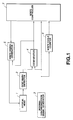
- Fig. 1 is a block diagram showing an embodiment of a data recording method and device for an optical memory card according to the invention.
- Fig. 1 when a non-illustrated optical memory card is inserted into a non-illustrated optical memory card reader/writer, the optical memory card reader/writer starts to record data and moves the optical memory card back and forth.
- An optical head 1 scans a recording region of the optical memory card, and the detected output is put in an SYNC mark detecting circuit 2.
- the SYNC mark detecting circuit 2 generates an SYNC mark detection signal, which produces a pulse upon detecting an SYNC mark, and enters it into a comparison circuit 4.
- An internal synchronization signal (frame synchronization signal) produced by an internal synchronization signal generating circuit 3 is entered into the comparison circuit 4, where it is detected whether the SYNC mark detection signal agrees with the internal synchronization signal, and if it does, it is judged that a card conveying rate has been synchronized with an electric circuit, and a synchronization lock signal is entered into a write signal generating circuit 5 and a write control circuit 7.
- the write signal generating circuit 5 According to a data signal output from the write control circuit 7 and a synchronization lock signal output from the comparison circuit 4, the write signal generating circuit 5 enters a signal for forming a record pit on the non-illustrated optical memory card into the optical head 1.
- a write cycle counter 6 counts a write cycle based on an internal synchronization signal output from the internal synchronization signal generating circuit 3 and outputs a write cycle signal to a write control circuit 7.
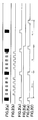
- Fig. 2 is a diagram showing record pit-formed positions and respective signals when a synchronization failure has occurred during data recording.
- Fig. 2 (a) shows positions of record pits on the optical memory card
- Fig. 2 (b) a write signal
- Fig. 2 (c) an SYNC mark detecting signal
- Fig. 2 (d) a synchronization lock signal
- Fig. 2 (e) an internal lock signal
- Fig. 2 (f) a write cycle a write cycle.
- the SYNC mark detection signal (see Fig. 2 (c)) output from the SYNC mark detection circuit 2 and the internal synchronization signal (see Fig. 2 (e) generated from the internal synchronization signal generating circuit 3 have the same pulse position. Accordingly, the synchronization lock signal (see Fig. 2 (d)) generated by the comparison circuit 4 is in a lock state indicating that synchronization has been made.
- the write signal generation circuit 5 outputs a write signal (see Fig. 2 (b)) for generating a pulse at a position where a record pit is formed according to the control made by the write control circuit 7, and based on the write signal, the optical head 1 forms the record pits on the optical memory card.
- the synchronization lock signal produced by the comparison circuit 4 falls in an unlock state indicating that the synchronization has been lost, because the SYNC mark detection signal and the internal synchronization signal have a different pulse generation position.
- the write signal generation circuit 5 stops the generation of the write signal, thereby stopping formation of the record pit (data recording).
- Fig. 3 is a diagram showing respective signals during rewrite operation performed immediately after stopping writing in the write cycle N shown in Fig. 2.
- Fig. 3 (a) through Fig. 3 (f) correspond to Fig. 2 (a) through Fig. 2 (f), respectively.
- the rewrite operation prevents the recording capacity of the optical memory card from being degraded, so that recording of data is started from a frame next to the frame which has caused a recording error due to the synchronization failure, namely from a write cycle N+1.
- Fig. 4 is a diagram showing an example of record with an SYNC mark lost (including undetectable) due to dust, a scratch or the like on a recording region of an optical memory card.
- Fig. 4 (a) through Fig. 4 (e) correspond to Fig. 2 (a) through Fig. 2 (e), respectively.
- the SYNC mark detection signal does not include a pulse as shown in Fig. 4 (c).
- the SYNC mark detection signal does not agree with the internal synchronization signal, and the synchronization lock signal output from the comparison circuit 4 indicates an unlock state.
- the comparison circuit 4 outputs a synchronization lock signal indicating the lock state even if the SYNC mark is not detected as shown in Fig. 4 (c) through Fig. 4 (e), and when the SYNC mark is detected, it is judged whether the synchronization is normal or not.
- the comparison circuit 4 outputs the synchronization lock signal in the unlock state to stop recording of data only when the SYNC mark detection signal having an apparent synchronization failure and the internal synchronization signal have a different pulse position.
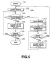
- Fig. 5 is a flowchart showing details of signal processing in the embodiment shown in Fig. 1.
- an unillustrated optical memory card reader/writer starts write operation (step 101), and when the synchronization lock signal output from the comparison circuit 4 indicates a synchronization lock state, the optical head 1 forms a record pit on the unillustrated optical memory card based on the write signal output from the write signal generation circuit 5 (step 102).
- synchronization lock signal indicates the synchronization lock state (YES in step 103)
- recording of data on the unillustrated optical memory card is continued, and the write cycle counter 6 counts rising edges of the internal synchronization signal and increases write cycle number n for each cycle of the internal synchronization signal (step 104).
- step 103 Operation from step 103 is repeated until all data is recorded (No in step 105).
- the unillustrated optical memory card reader/writer Upon recording of all data (YES in step 105), the unillustrated optical memory card reader/writer terminates the write operation.
- the write signal generation circuit 5 stops the write signal (step 107), the value of write cycle number n is retained as an out-of-synchronization write cycle N (step 108), and rewrite operation is started.
- the rewrite operation starts recording from a frame with write cycle number N+1 adjacent to the frame with write cycle number N where a record error has occurred due to out-of-synchronization. Therefore, the card is carried until write cycle number n becomes N+1 (NO in step 109) to increase write cycle number n for every cycle of an internal synchronization signal (step 110).
- step 109 When write cycle number n becomes N+1 (YES in step 109), the step returns to step 102 to restart the write operation, and a record pit is formed on the optical memory card.
- the invention can be applied to a data recording method and device for an optical memory card.
- the invention is configured to compare a synchronization signal, which is obtained by detecting an SYNC mark during data recording, with an internal synchronization signal, which is generated in a card reader/writer, and if synchronization is lost, to stop data recording, and to restart data recording from a frame adjacent to the frame which has caused a data recording error.
- a recording capacity of the optical memory card can be prevented from being lowered.
- the data recorded in the frame which has caused the data recording error is corrected based on an error correction code which was recorded together with the data on the optical memory card, so that it is not necessary to rerecord data, and a data recording region of the optical memory card can be used effectively.
Landscapes
- Engineering & Computer Science (AREA)
- Signal Processing (AREA)
- Physics & Mathematics (AREA)
- General Physics & Mathematics (AREA)
- Theoretical Computer Science (AREA)
- Optical Recording Or Reproduction (AREA)
- Signal Processing For Digital Recording And Reproducing (AREA)
Applications Claiming Priority (3)
| Application Number | Priority Date | Filing Date | Title |
|---|---|---|---|
| JP8298783A JPH10144009A (ja) | 1996-11-11 | 1996-11-11 | 光メモリカードのデータ記録方法および装置 |
| JP298783/96 | 1996-11-11 | ||
| PCT/JP1997/004082 WO1998021721A1 (en) | 1996-11-11 | 1997-11-10 | Data recording method and apparatus for optical memory cards |
Publications (2)
| Publication Number | Publication Date |
|---|---|
| EP0874366A1 true EP0874366A1 (de) | 1998-10-28 |
| EP0874366A4 EP0874366A4 (de) | 2006-05-24 |
Family
ID=17864170
Family Applications (1)
| Application Number | Title | Priority Date | Filing Date |
|---|---|---|---|
| EP97911499A Withdrawn EP0874366A4 (de) | 1996-11-11 | 1997-11-10 | Datenaufzeichnungsverfahren und -gerät für optische speicherdaten |
Country Status (7)
| Country | Link |
|---|---|
| US (1) | US6282159B1 (de) |
| EP (1) | EP0874366A4 (de) |
| JP (1) | JPH10144009A (de) |
| KR (1) | KR19990076999A (de) |
| CN (1) | CN1208492A (de) |
| CA (1) | CA2242164C (de) |
| WO (1) | WO1998021721A1 (de) |
Families Citing this family (4)
| Publication number | Priority date | Publication date | Assignee | Title |
|---|---|---|---|---|
| JP3994708B2 (ja) * | 2001-09-17 | 2007-10-24 | ティアック株式会社 | 光ディスク装置 |
| US7151732B2 (en) * | 2001-10-30 | 2006-12-19 | Ricoh Company, Ltd. | Optical disk unit capable of reading out data normally and continuously after suspension of data writing |
| JP5313576B2 (ja) * | 2008-07-18 | 2013-10-09 | エイチジーエスティーネザーランドビーブイ | 磁気ディスク装置及びその制御方法 |
| JP2024132586A (ja) | 2023-03-17 | 2024-10-01 | 株式会社東芝 | 磁気ディスク装置 |
Family Cites Families (13)
| Publication number | Priority date | Publication date | Assignee | Title |
|---|---|---|---|---|
| CA1294705C (en) * | 1986-04-09 | 1992-01-21 | Wataru Sakagami | Optical information recording medium and recording-reproducing apparatus |
| US4910725A (en) * | 1986-04-23 | 1990-03-20 | Drexler Technology Corporation | Optical recording method for data cards |
| US4885458A (en) * | 1987-02-04 | 1989-12-05 | Olympus Optical Co., Ltd. | Card-form recording medium and data recording device therefor |
| JPS63193379A (ja) * | 1987-02-05 | 1988-08-10 | Nec Corp | デイスク装置 |
| JPH01282730A (ja) * | 1988-05-07 | 1989-11-14 | Sharp Corp | 光学記録再生装置 |
| JPH02166673A (ja) * | 1988-12-20 | 1990-06-27 | Csk Corp | 光記録媒体 |
| JP2725197B2 (ja) * | 1989-02-23 | 1998-03-09 | オムロン株式会社 | 光学的記録再生装置 |
| US5175655A (en) * | 1989-07-17 | 1992-12-29 | Canon Kabushiki Kaisha | Method and apparatus for verifying a signal recorded in an encoded form on a medium |
| JPH03156775A (ja) * | 1989-08-30 | 1991-07-04 | Canon Inc | 情報記録方法及び情報記録装置 |
| JP3210323B2 (ja) * | 1990-08-03 | 2001-09-17 | キヤノン株式会社 | Resync検出回路 |
| JPH04134670A (ja) * | 1990-09-25 | 1992-05-08 | Olympus Optical Co Ltd | データ記録再生装置 |
| JP3109708B2 (ja) * | 1994-05-19 | 2000-11-20 | キヤノン株式会社 | 光学的情報記録再生装置 |
| JP3156775B2 (ja) | 1998-06-18 | 2001-04-16 | 日本電気株式会社 | 軽量立体形導波路 |
-
1996
- 1996-11-11 JP JP8298783A patent/JPH10144009A/ja active Pending
-
1997
- 1997-11-10 CN CN97191674A patent/CN1208492A/zh active Pending
- 1997-11-10 KR KR1019980705129A patent/KR19990076999A/ko not_active Ceased
- 1997-11-10 CA CA002242164A patent/CA2242164C/en not_active Expired - Fee Related
- 1997-11-10 WO PCT/JP1997/004082 patent/WO1998021721A1/ja not_active Ceased
- 1997-11-10 EP EP97911499A patent/EP0874366A4/de not_active Withdrawn
- 1997-11-10 US US09/101,747 patent/US6282159B1/en not_active Expired - Fee Related
Also Published As
| Publication number | Publication date |
|---|---|
| CN1208492A (zh) | 1999-02-17 |
| EP0874366A4 (de) | 2006-05-24 |
| US6282159B1 (en) | 2001-08-28 |
| JPH10144009A (ja) | 1998-05-29 |
| KR19990076999A (ko) | 1999-10-25 |
| CA2242164A1 (en) | 1998-05-22 |
| WO1998021721A1 (en) | 1998-05-22 |
| CA2242164C (en) | 2001-05-15 |
Similar Documents
| Publication | Publication Date | Title |
|---|---|---|
| EP0603949B1 (de) | Datenaufzeichnungsgerät mit Segmentsynchronisation | |
| EP0139757B1 (de) | Vorrichtung zur wiedergabe von signaldaten | |
| EP0553409B1 (de) | Verfahren und Gerät zur Erzeugung von Servomarken | |
| US4663752A (en) | Sector mark signal control circuit for disc apparatus | |
| US5353175A (en) | Apparatus for using window signal generators to enable detection of header information such as an address mark, sector mark, or address information recorded on each sector of a disc recording medium only where such information could be present | |
| US6483789B1 (en) | Data recording and/or reproducing apparatus and method for detecting sector defects | |
| US5363360A (en) | Method and apparatus for detecting and processing synchronization marks extracted from a prerecorded wobbled groove on a compact disk | |
| CA2242164C (en) | Data recording method and apparatus for optical memory cards | |
| JPH04134670A (ja) | データ記録再生装置 | |
| US5359584A (en) | Data recording/reproducing method and apparatus having means for reliable detection of unrecorded sectors | |
| US6557141B1 (en) | Magnetic media certification | |
| US5202877A (en) | Apparatus for detecting unused sector on record medium | |
| US5796794A (en) | Method and apparatus for serial-to-parallel conversion of data based on sync recovery | |
| US5237550A (en) | Reloadable optical recording/reproducing apparatus | |
| US5363252A (en) | Method and system for track skew tolerant acquistion burst sequence validation in a data storage system | |
| US7406009B2 (en) | Information recording/reproducing apparatus and information reproducing method | |
| JPH0834047B2 (ja) | 磁気記録再生装置 | |
| GB2054944A (en) | Apparatuses for and methods for detecting splicing points in magnetic media | |
| EP0580306B1 (de) | Band-Aufzeichnungs- und/oder -Wiedergabegerät | |
| US5583708A (en) | Circuit for detecting unrecorded portion of recording medium | |
| JP3321884B2 (ja) | 同期ブロック検出方法および同期ブロック検出装置 | |
| CN100363988C (zh) | 信息记录方法及装置、信息重放方法及装置 | |
| JPH03156775A (ja) | 情報記録方法及び情報記録装置 | |
| JP2882611B2 (ja) | 追記型光学式記録再生装置 | |
| JP3598838B2 (ja) | データ読み取り装置 |
Legal Events
| Date | Code | Title | Description |
|---|---|---|---|
| PUAI | Public reference made under article 153(3) epc to a published international application that has entered the european phase |
Free format text: ORIGINAL CODE: 0009012 |
|
| AK | Designated contracting states |
Kind code of ref document: A1 Designated state(s): DE FR GB |
|
| 17P | Request for examination filed |
Effective date: 19981118 |
|
| A4 | Supplementary search report drawn up and despatched |
Effective date: 20060406 |
|
| STAA | Information on the status of an ep patent application or granted ep patent |
Free format text: STATUS: THE APPLICATION HAS BEEN WITHDRAWN |
|
| 18W | Application withdrawn |
Effective date: 20060630 |