EP0869611B1 - Faster switching GaAs fet switches by illumination with high intensity light - Google Patents
Faster switching GaAs fet switches by illumination with high intensity light Download PDFInfo
- Publication number
- EP0869611B1 EP0869611B1 EP98101556A EP98101556A EP0869611B1 EP 0869611 B1 EP0869611 B1 EP 0869611B1 EP 98101556 A EP98101556 A EP 98101556A EP 98101556 A EP98101556 A EP 98101556A EP 0869611 B1 EP0869611 B1 EP 0869611B1
- Authority
- EP
- European Patent Office
- Prior art keywords
- gaas
- switches
- step attenuator
- leds
- light
- Prior art date
- Legal status (The legal status is an assumption and is not a legal conclusion. Google has not performed a legal analysis and makes no representation as to the accuracy of the status listed.)
- Expired - Lifetime
Links
Images


Classifications
-
- H—ELECTRICITY
- H10—SEMICONDUCTOR DEVICES; ELECTRIC SOLID-STATE DEVICES NOT OTHERWISE PROVIDED FOR
- H10F—INORGANIC SEMICONDUCTOR DEVICES SENSITIVE TO INFRARED RADIATION, LIGHT, ELECTROMAGNETIC RADIATION OF SHORTER WAVELENGTH OR CORPUSCULAR RADIATION
- H10F55/00—Radiation-sensitive semiconductor devices covered by groups H10F10/00, H10F19/00 or H10F30/00 being structurally associated with electric light sources and electrically or optically coupled thereto
- H10F55/20—Radiation-sensitive semiconductor devices covered by groups H10F10/00, H10F19/00 or H10F30/00 being structurally associated with electric light sources and electrically or optically coupled thereto wherein the electric light source controls the radiation-sensitive semiconductor devices, e.g. optocouplers
- H10F55/25—Radiation-sensitive semiconductor devices covered by groups H10F10/00, H10F19/00 or H10F30/00 being structurally associated with electric light sources and electrically or optically coupled thereto wherein the electric light source controls the radiation-sensitive semiconductor devices, e.g. optocouplers wherein the radiation-sensitive devices and the electric light source are all semiconductor devices
Definitions
- the present invention relates to Gallium Arsenide (GaAs) Field Effect Transistor (FET) switches for use, for example, in microwave test equipment.
- GaAs Gallium Arsenide
- FET Field Effect Transistor
- Microwave test equipment has traditionally used mechanically switched step attenuators to set the output level of sources and network analyzers. These switches were very low loss, but they had drawbacks in terms of switching speed (on the order of 30 milliseconds), size, and reliability.
- GaAs FET IC Integrated Circuit
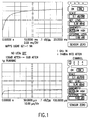
- GaAs FET based IC microwave switches continue to have what is known as the "slow tail effect" which causes the amplitude of the switched microwave signal to only gradually come to its final value after a period of 15 to 20 milliseconds after the switch is turned to the ON state, such as shown in Figure 1.
- the explanation usually given for this effect is that traps in the GaAs caused by the exposed GaAs surface in a FET structure have a time constant on the order of milliseconds. The number and time constants of these traps are extremely dependent on the GaAs wafer processing, and can vary from less than one millisecond to much greater in a fairly unpredictable manner, even between wafers processed through the same process but at different times.
- the channel under the FET gate is depleted of electrons, and each trap has a high probability of having a captured electron with it.
- the FET When the FET is turned ON, the Fermi level shifts and the electrons captured by the traps are released and enter the channel along with the electrons attracted from the standard donor atoms.
- the traps release their electrons with a time constant on the order of milliseconds, the electron contribution from the traps to the channel does not reach equilibrium until 10 to 20 milliseconds after switching has occurred.
- the conductivity of the FET channel, and hence the attenuation of the microwave signal passing through the FET channel are not stable until 10 to 20 milliseconds after switching.
- the traps involved in slow tails are due mainly to the influence of the surface region around the gate, as described for example in R. Yeats et al, "Gate Slow Transients in GaAs MESFETS - Causes, Cures, and Impact on Circuits", 1988 IEDM Conference Proceedings, pp 842-845.
- Slow tails can be minimized at the device level by making the recess in the GaAs for the gate tighter and/or by using moderate to high doping near the edges of the gate.
- both of these techniques are detrimental to the power handling capability of the GaAs FET. Since it is desirable to have high output powers from microwave test equipment sources, degrading the power handling capability of the switches on the output step attenuator of the instrument is undesirable.
- US-A-5,347,239 discloses a step attenuator including an attenuation network having two inputs and two outputs, permitting four different attenuation levels to be selected by use of just one input switch and one output switch.
- the input switch and output switch are formed by GaAsFET switching devices.
- JP-A-63055978 relates to a semiconductor device including a GaAs-MESFET chip including two GaAs-MESFETs to the surfaces of which light is emitted by means of a light-emitting element.
- the present invention provides an improved step attenuator device which comprises a GaAsFETIC switch arrangement including a plurality of GaAsFETIC switches, which would normally exhibit a slow tail effect when in operation, in combination with a plurality of light sources (LEDs) located within the step attenuator device where each of the light sources corresponds to a respective one of the GaAs switches and has a sufficient light intensity for illuminating the respective GaAs switch during operation so as to reduce or minimize the slow tail effect.
- LEDs light sources
- GaAs FET based IC microwave switches exhibit what has been described above as the "slow tail effect" which causes the amplitude of the switched microwave signal to only gradually come to its final value after a period of 15 to 20 milliseconds after the switch is turned ON, such as shown in Figure 1.
- the advantages of reliability and compactness are preserved, while eliminating the drawback of slow settling on the output amplitude. It is a well known phenomena that shining a light on GaAs FET switches affects their slow tails. In fact, some tests on GaAs FET IC switches are actually performed in darkened chambers to give accurate correlation with the performance of the IC switch in its final sealed, dark package.
- Figure 2 shows an assembled GaAs FET IC 130 dB step attenuator package 10 with LEDs 15 according to the present invention
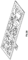
- Figure 3A shows an exploded view an the GaAs FET IC step attenuator 10 of Figure 2
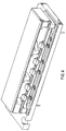
- Figure 4 shows a cutaway view of the GaAs FET IC step attenuator 10 of Figure 2.
- the GaAs FET IC 130 dB step attenuator 10 comprises a GaAs switch arrangement which includes a base circuit 20 which further includes or contains a plurality of gallium arsenide switches 21 (shown in better view in Figure 4).
- the step attenuator of Figure 4 includes five GaAs switches 21 (21-1; 21-2; 21-3; 21-4; and 21-5).
- the step attenuator 10 of Figure 3A and particularly the GaAs switch arrangement shows the base circuit 20 containing the GaAs FET IC switches 21 with a lid preform 22 that contains silicone-encapsulant.
- Lid preform 22 is a conductive epoxy preform that attaches the lid 23 to the ceramic circuit, which is typically made of alumina.
- Conductive epoxy preform 24 is placed on top of lid 23.
- Preform 24 attaches PC board 25 to the bottom lid 23.
- PC board 25 includes a plurality of super-bright LEDs 15. In one preferred embodiment, five LEDs 15 are used, which correspond to the five GaAs switches 21.
- the LEDs 15 are shown separated from PC board 25. In one preferred embodiment, there are five LED's 15 (15-1; 15-2; 15-3; 15-4; 15-5), one for each gallium arsenide IC switch of circuit 21 (21-1; 21-2; 21-3; 21-4; 21-5). When used, the LEDs 15 are attached to the PC board 25, but are shown separated in Figure 3A, for clarity purposes.
- the super-bright LEDs 15 include biasing and decoupling circuitry (shown in Figure 3B), which prevents microwave energy from propagating through the LEDs 15 to the output.
- biasing and decoupling circuitry shown in Figure 3B
- the PC board 25 includes LEDs 15 and in addition includes capacitors, ferrites and resistors arranged in a normal fashion as to eliminate the feedthrough down to extremely low levels, so as to provide a clean output signal with very little ripple.
- PC board 25 is attached with a PC board conductive epoxy preform 26 to middle lid 27.
- Middle lid 27 is used as a container so that the upper region can be silicone encapsulated to prevent moisture from degrading the performance and causing silver migration, which allows the device operate safely in extremely humid environments.
- Conductive epoxy preform 28 is used to attach the top lid 29 to middle lid 27, and serves to keep out stray RF signals from coming in and keep RF signals from propagating out and causing interference in other regions of the microwave instrument.
- the GaAs switches 21 on the IC are set to form a low insertion loss "thru" path, called the 0 dB state.
- the GaAs switches on the IC switch in a higher insertion loss state.
- the high insertion loss can be defined in dB increments (e.g., 10 dB, 20 dB, 40 dB) in which different levels of attenuation can be switched in an out.
- the step attenuator 10 of Figure 3A comprises a 130 dB step attenuator which can be in any state of attenuation in five dB steps or increments between zero and 130 dB, by switching in and out the various segments (or GaAs switches 21).
- gallium arsenide switches exhibit what is called the slow tail effect.
- the step attenuator When switched between the OFF state to the ON state, the step attenuator does not reach full conductivity in the FET channel in the ON state for typically 10-20 milliseconds.
- the insertion loss through the device slowly changes before reaching the equilibrium value, as shown in Figure 1. This settling time causes unwanted delays, especially for modulation standards that should be switched and settled within, say, 20 microseconds.
- the slow tail effect improves markedly such that the slow tails effect went away by a factor of about a hundredfold faster than in prior art approaches.
- the magnitude of the slow tail effect for a 5 or 10 microsecond time interval may be improved by a factor of two, but the point in time at which the slow tail effect disappeared to within .018 dB improved by a factor of about 100.
- a sufficiently bright light source such as a super-bright LED is integrated with the GaAs switch arrangement to form a step attenuator package which improves the slow tail effect described above and still maintain a low-cost package.
- super-bright LEDs are presently now available, such as from the Hewlett-Packard Company. The effect with super-bright LEDs is intensity dependent -- the brighter the light, the more the slow tail effect goes away.
- the preferred intensity level of the super-bright LEDs 15 of Figures 3A and 4 is rated at approximately 500 millicandles, with a half-angle of 28 degrees.
- the miniaturized high-intensity LEDs 15 in Figure 3A are able to shine enough light directly over the GaAs switches 21 to minimize or in some instances eliminate the slow tail effect.
- the present invention is believed to be suitable with super-bright LEDs with a light intensity of approximately 500 millicandles at a 28 half-degree angle of light output and where each LED 15 is positioned or located at a certain distance above the corresponding GaAs IC switch 21.
- the preferred distance between each LED 15 and the corresponding GaAs IC switch 21 is 3 to 3-1/2 millimeters, as a typical example.
- a clear silicone encapsulant surrounds the package so that the package is moisture resistant. Also, the package is designed with the clear silicone encapsulant and reflective metal surfaces so as to take advantage of reflected light (typically, all the metal surfaces are gold plated).
- the ability to use LEDS is preserved. If dark-colored encapsulant or an opaque encapsulant is used, the use of the LEDs is no longer possible.
- Step attenuators are made with fixed resistors that are switched in and out with gallium arsenide switches which have rapid response times between the OFF state to the ON state. There is a time transition from high-impedance to low-impedance states, and the use of integrated super-bright LEDS accelerates the response time.
- the GaAs FET switches 21 control the switching in and out the resistors, and the use of the super-bright LEDs 15 shining permanently on the GaAs FET switches 21 has a very beneficial effect on the response time.
- FIG 4 there is a single LED 15 positioned directly over each gallium arsenide IC switch 21.
- the GaAs IC switches 21 are all bathed in reflected light from all of the different LEDs 15. If one LED 15 fails (say LED 15-2), the corresponding GaAs IC switch 21-2 that was being illuminated does not go back to its worst-case operating condition. Instead; GaAS IC switch 21-2 exhibits a graceful degradation mode, which would not be the case if only a single light source were used (which would result in failure).
- the redundancy aspect of five LEDs 15 placed directly over the GaAs switches 21 avoids the problems involved if a single light source goes out, and the very small LEDs allows the light source to be placed very close to the circuits.
- the failure of one LED would not affect the slow-tails performance as much as if there were no illumination at all.
- the light sources utilized with the present invention are desirably of a sufficiently small size (such as super-bright LEDs 15) in order to keep the compactness of the original small package structure, and also in order to provide shielding between various segments of the circuit.
- a sufficiently small size such as super-bright LEDs 15
- LEDs 15 are cooler, and provide DC current efficiency; so that a large power supply is not needed for the device.
- the redundancy aspect of five LEDs 15 placed directly over the GaAs switches 21 avoids the problems involved if a single light source goes out, and the very small LEDs allows the light source to be placed very close to the circuits.
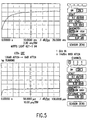
- Figure 5 shows the response of the GaAs FET IC switched 130 dB step attenuator 10 with all the sections being switched simultaneously (going from the 130 dB attenuation state to the 0 dB attenuation state) and with the LEDs 15 (which are mounted over the corresponding switch 21) turned OFF. It can be seen that the amplitude of the signal is still increasing at 20 milliseconds (near the end of the plot of Figure 5).
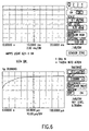
- Figure 6 shows a view of the slow tail effect of the step attenuator 10 of Figure 2 with the LEDs 21 turned ON.
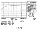
- the same step attenuator 10 settles to within .018 dB in 120 microseconds, as shown in Figures 8A and 8B.
- the amplitude settling time of the step attenuator 10 has thus been speeded up by a factor of 183.
- a high intensity light can repeatably, and to a high degree, reduce the "slow tail” phenomena in GaAs FET based switches and step attenuators.
- This desirable aspect allows the output amplitude of a GaAs switch to settle to its final value much more rapidly.
- the "slow tail" phenomena of a packaged product containing GaAs FET based switches can be greatly reduced, while the size and cost of the package are not greatly increased.
- the noise figures of some amplifiers has been lowered by shining the light directly on the amplifier, and having a bright-intensity light that produces very little heat that can be positioned directly over amplifier chips in a gallium arsenide IC would provide the benefit of lower noise and possibly higher gain. Also in travelling wave amplifiers made of gallium arsenide IC's, shining bright light directly on those has eliminated slow tail effects in switching transients when utilized in an on/off pulse mode. Also, high-intensity light shined on certain devices such as negative-resistance devices and varactors could improve the 1/F or phase-noise characteristics.
- gallium arsenide amplifiers can be improved.
- gallium arsenide amplifiers are not used at low frequencies because they have a very high [1/F] noise component, which means as the frequencies goes down, there is more noise on the signal.
- This noise is generally associated with at least some portions of the traps emptying and filling. If the traps are emptied by shining the light directly those traps, the photons eject the electrons. This noise component could be greatly improved and extend the utility of gallium arsenide amplifiers to lower frequencies.
Landscapes
- Led Devices (AREA)
- Non-Reversible Transmitting Devices (AREA)
- Attenuators (AREA)
- Networks Using Active Elements (AREA)
- Junction Field-Effect Transistors (AREA)
Applications Claiming Priority (2)
| Application Number | Priority Date | Filing Date | Title |
|---|---|---|---|
| US829924 | 1997-04-01 | ||
| US08/829,924 US5808322A (en) | 1997-04-01 | 1997-04-01 | Faster switching GaAs FET switches by illumination with high intensity light |
Publications (2)
| Publication Number | Publication Date |
|---|---|
| EP0869611A1 EP0869611A1 (en) | 1998-10-07 |
| EP0869611B1 true EP0869611B1 (en) | 2001-07-25 |
Family
ID=25255917
Family Applications (1)
| Application Number | Title | Priority Date | Filing Date |
|---|---|---|---|
| EP98101556A Expired - Lifetime EP0869611B1 (en) | 1997-04-01 | 1998-01-29 | Faster switching GaAs fet switches by illumination with high intensity light |
Country Status (4)
| Country | Link |
|---|---|
| US (1) | US5808322A (enExample) |
| EP (1) | EP0869611B1 (enExample) |
| JP (1) | JPH118525A (enExample) |
| DE (1) | DE69801177T2 (enExample) |
Families Citing this family (13)
| Publication number | Priority date | Publication date | Assignee | Title |
|---|---|---|---|---|
| DE10228810B4 (de) * | 2002-06-27 | 2010-09-30 | Rohde & Schwarz Gmbh & Co. Kg | Mikrowellen-Schaltung mit beleuchteten Feldeffekt-Transistoren |
| DE102004024367A1 (de) * | 2004-05-17 | 2005-12-22 | Rohde & Schwarz Gmbh & Co. Kg | Kalibrierbare Mikrowellen-Schaltung mit beleuchtbaren GaAs-FET sowie Kalibriervorrichtung und Verfahren zur Kalibrierung |
| US7847301B2 (en) * | 2004-12-08 | 2010-12-07 | Agilent Technologies, Inc. | Electronic microcircuit having internal light enhancement |
| US8022519B2 (en) | 2005-05-19 | 2011-09-20 | Sandisk Technologies Inc. | System-in-a-package based flash memory card |
| US20070126525A1 (en) * | 2005-12-01 | 2007-06-07 | Nicholson Dean B | Dual path attenuation system |
| JP4935373B2 (ja) * | 2007-01-23 | 2012-05-23 | 横河電機株式会社 | スイッチ回路およびこのスイッチ回路を用いたステップアッテネータ |
| WO2016198100A1 (en) | 2015-06-10 | 2016-12-15 | Advantest Corporation | High frequency integrated circuit and emitting device for irradiating the integrated circuit |
| US9590591B1 (en) * | 2016-03-17 | 2017-03-07 | Analog Devices Global | High frequency signal attenuators |
| US10326018B1 (en) | 2018-02-28 | 2019-06-18 | Nxp Usa, Inc. | RF switches, integrated circuits, and devices with multi-gate field effect transistors and voltage leveling circuits, and methods of their fabrication |
| US10784862B1 (en) | 2019-09-10 | 2020-09-22 | Nxp Usa, Inc. | High speed switching radio frequency switches |
| US10972091B1 (en) | 2019-12-03 | 2021-04-06 | Nxp Usa, Inc. | Radio frequency switches with voltage equalization |
| US11368180B2 (en) | 2020-07-31 | 2022-06-21 | Nxp Usa, Inc. | Switch circuits with parallel transistor stacks and methods of their operation |
| US11683028B2 (en) | 2021-03-03 | 2023-06-20 | Nxp Usa, Inc. | Radio frequency switches with voltage equalization |
Family Cites Families (7)
| Publication number | Priority date | Publication date | Assignee | Title |
|---|---|---|---|---|
| US3043958A (en) * | 1959-09-14 | 1962-07-10 | Philips Corp | Circuit element |
| DE1190506B (de) * | 1963-10-10 | 1965-04-08 | Siemens Ag | Optisch gesteuerte, mindestens vier Zonen von abwechselnd unterschiedlichem Leitungstyp aufweisende Schalt- oder Kippdiode |
| JPS5457983A (en) * | 1977-10-18 | 1979-05-10 | Toshiba Corp | Optical semiconductor device |
| JPS6355978A (ja) * | 1986-08-26 | 1988-03-10 | Yokogawa Electric Corp | 半導体装置 |
| JP2629428B2 (ja) * | 1990-10-01 | 1997-07-09 | 日本電気株式会社 | 砒化ガリウムfet集積回路 |
| JPH05226688A (ja) * | 1992-01-08 | 1993-09-03 | Nec Corp | フォトカプラ |
| US5347239A (en) * | 1992-12-03 | 1994-09-13 | Hewlett-Packard Company | Step attenuator |
-
1997
- 1997-04-01 US US08/829,924 patent/US5808322A/en not_active Expired - Fee Related
-
1998
- 1998-01-29 DE DE69801177T patent/DE69801177T2/de not_active Expired - Fee Related
- 1998-01-29 EP EP98101556A patent/EP0869611B1/en not_active Expired - Lifetime
- 1998-03-19 JP JP10070883A patent/JPH118525A/ja active Pending
Also Published As
| Publication number | Publication date |
|---|---|
| EP0869611A1 (en) | 1998-10-07 |
| DE69801177T2 (de) | 2002-03-21 |
| US5808322A (en) | 1998-09-15 |
| JPH118525A (ja) | 1999-01-12 |
| DE69801177D1 (de) | 2001-08-30 |
Similar Documents
| Publication | Publication Date | Title |
|---|---|---|
| EP0869611B1 (en) | Faster switching GaAs fet switches by illumination with high intensity light | |
| US20060118807A1 (en) | Electronic microcircuit having internal light enhancement | |
| US5057805A (en) | Microwave semiconductor device | |
| US3585455A (en) | Circuit assemblies | |
| EP1182704A3 (en) | High frequency module | |
| EP0438056A2 (en) | High-Frequency circuit package | |
| EP1189279A4 (en) | SEMI-FINISHED SEMICONDUCTOR ARRANGEMENT, CIRCUIT UNIT FOR ARRANGEMENT, AND MANUFACTURING METHOD FOR CIRCUIT UNIT | |
| GB2273217A (en) | Step attenuator | |
| EP0149317A2 (en) | Circuit packaging | |
| US6876271B2 (en) | Microwave switching with illuminated field effect transistors | |
| US6483175B2 (en) | Wiring board and semiconductor device using the same | |
| US6294971B1 (en) | Inverted board mounted electromechanical device | |
| EP0591402A1 (en) | Active superconductive devices | |
| JP7124214B2 (ja) | レーザ装置およびレーザ装置の製造方法 | |
| KR20070099441A (ko) | 발광 유닛 및 조명 장치 | |
| KR19990077001A (ko) | 반도체 디바이스 | |
| US20070126525A1 (en) | Dual path attenuation system | |
| KR910009139B1 (ko) | 광모듈 | |
| IT1062029B (it) | Dispositivo e procedimento di incapsulamento e montaggio di moduli elettronici | |
| McLevige et al. | Microwave switching with parallel-resonated GaAs FETs | |
| US8796801B2 (en) | Illuminable GaAs switching component with transparent housing and associated microwave circuit | |
| US5920065A (en) | Optically activated back-to-back PIN diode switch having exposed intrinsic region | |
| Ota et al. | High isolation and low insertion loss switch IC using GaAs MESFET's | |
| EP2063484B1 (en) | Microwave module | |
| Poitrenaud et al. | A novel 5-30GHz voltage controlled variable attenuator with high linearity in a low cost SMD compact package |
Legal Events
| Date | Code | Title | Description |
|---|---|---|---|
| PUAI | Public reference made under article 153(3) epc to a published international application that has entered the european phase |
Free format text: ORIGINAL CODE: 0009012 |
|
| AK | Designated contracting states |
Kind code of ref document: A1 Designated state(s): DE GB |
|
| 17P | Request for examination filed |
Effective date: 19990129 |
|
| 17Q | First examination report despatched |
Effective date: 19990324 |
|
| AKX | Designation fees paid |
Free format text: DE GB |
|
| GRAG | Despatch of communication of intention to grant |
Free format text: ORIGINAL CODE: EPIDOS AGRA |
|
| GRAG | Despatch of communication of intention to grant |
Free format text: ORIGINAL CODE: EPIDOS AGRA |
|
| GRAG | Despatch of communication of intention to grant |
Free format text: ORIGINAL CODE: EPIDOS AGRA |
|
| GRAH | Despatch of communication of intention to grant a patent |
Free format text: ORIGINAL CODE: EPIDOS IGRA |
|
| GRAH | Despatch of communication of intention to grant a patent |
Free format text: ORIGINAL CODE: EPIDOS IGRA |
|
| RAP1 | Party data changed (applicant data changed or rights of an application transferred) |
Owner name: HEWLETT-PACKARD COMPANY, A DELAWARE CORPORATION |
|
| GRAA | (expected) grant |
Free format text: ORIGINAL CODE: 0009210 |
|
| AK | Designated contracting states |
Kind code of ref document: B1 Designated state(s): DE GB |
|
| RAP2 | Party data changed (patent owner data changed or rights of a patent transferred) |
Owner name: AGILENT TECHNOLOGIES INC. |
|
| RAP2 | Party data changed (patent owner data changed or rights of a patent transferred) |
Owner name: AGILENT TECHNOLOGIES INC. A DELAWARE CORPORATION |
|
| REF | Corresponds to: |
Ref document number: 69801177 Country of ref document: DE Date of ref document: 20010830 |
|
| RAP2 | Party data changed (patent owner data changed or rights of a patent transferred) |
Owner name: AGILENT TECHNOLOGIES, INC. (A DELAWARE CORPORATION |
|
| REG | Reference to a national code |
Ref country code: GB Ref legal event code: IF02 |
|
| PLBE | No opposition filed within time limit |
Free format text: ORIGINAL CODE: 0009261 |
|
| STAA | Information on the status of an ep patent application or granted ep patent |
Free format text: STATUS: NO OPPOSITION FILED WITHIN TIME LIMIT |
|
| 26N | No opposition filed | ||
| PGFP | Annual fee paid to national office [announced via postgrant information from national office to epo] |
Ref country code: DE Payment date: 20070228 Year of fee payment: 10 |
|
| GBPC | Gb: european patent ceased through non-payment of renewal fee |
Effective date: 20070129 |
|
| PG25 | Lapsed in a contracting state [announced via postgrant information from national office to epo] |
Ref country code: GB Free format text: LAPSE BECAUSE OF NON-PAYMENT OF DUE FEES Effective date: 20070129 |
|
| PG25 | Lapsed in a contracting state [announced via postgrant information from national office to epo] |
Ref country code: DE Free format text: LAPSE BECAUSE OF NON-PAYMENT OF DUE FEES Effective date: 20080801 |
|
| PGFP | Annual fee paid to national office [announced via postgrant information from national office to epo] |
Ref country code: GB Payment date: 20060127 Year of fee payment: 9 |