EP0864180B1 - Low resistance contact semiconductor diode - Google Patents
Low resistance contact semiconductor diode Download PDFInfo
- Publication number
- EP0864180B1 EP0864180B1 EP96939228A EP96939228A EP0864180B1 EP 0864180 B1 EP0864180 B1 EP 0864180B1 EP 96939228 A EP96939228 A EP 96939228A EP 96939228 A EP96939228 A EP 96939228A EP 0864180 B1 EP0864180 B1 EP 0864180B1
- Authority
- EP
- European Patent Office
- Prior art keywords
- layer
- doped
- type material
- type
- contact
- Prior art date
- Legal status (The legal status is an assumption and is not a legal conclusion. Google has not performed a legal analysis and makes no representation as to the accuracy of the status listed.)
- Expired - Lifetime
Links
- 239000004065 semiconductor Substances 0.000 title claims abstract description 22
- 239000000463 material Substances 0.000 claims abstract description 58
- 230000005855 radiation Effects 0.000 claims abstract description 14
- 230000003287 optical effect Effects 0.000 claims description 10
- 230000005669 field effect Effects 0.000 claims description 3
- 239000000758 substrate Substances 0.000 description 12
- WPYVAWXEWQSOGY-UHFFFAOYSA-N indium antimonide Chemical compound [Sb]#[In] WPYVAWXEWQSOGY-UHFFFAOYSA-N 0.000 description 7
- 229910052751 metal Inorganic materials 0.000 description 5
- 239000002184 metal Substances 0.000 description 5
- HBMJWWWQQXIZIP-UHFFFAOYSA-N silicon carbide Chemical compound [Si+]#[C-] HBMJWWWQQXIZIP-UHFFFAOYSA-N 0.000 description 4
- 229910010271 silicon carbide Inorganic materials 0.000 description 4
- 229910001218 Gallium arsenide Inorganic materials 0.000 description 3
- 238000010521 absorption reaction Methods 0.000 description 3
- 238000005253 cladding Methods 0.000 description 3
- 229910000661 Mercury cadmium telluride Inorganic materials 0.000 description 2
- 230000004888 barrier function Effects 0.000 description 2
- 230000008901 benefit Effects 0.000 description 2
- MCMSPRNYOJJPIZ-UHFFFAOYSA-N cadmium;mercury;tellurium Chemical compound [Cd]=[Te]=[Hg] MCMSPRNYOJJPIZ-UHFFFAOYSA-N 0.000 description 2
- 239000000969 carrier Substances 0.000 description 2
- 230000008859 change Effects 0.000 description 2
- 230000007423 decrease Effects 0.000 description 2
- 238000010586 diagram Methods 0.000 description 2
- 239000002019 doping agent Substances 0.000 description 2
- 230000007717 exclusion Effects 0.000 description 2
- 238000000605 extraction Methods 0.000 description 2
- 239000010931 gold Substances 0.000 description 2
- 238000004020 luminiscence type Methods 0.000 description 2
- 230000006798 recombination Effects 0.000 description 2
- 238000005215 recombination Methods 0.000 description 2
- 238000001228 spectrum Methods 0.000 description 2
- VYZAMTAEIAYCRO-UHFFFAOYSA-N Chromium Chemical compound [Cr] VYZAMTAEIAYCRO-UHFFFAOYSA-N 0.000 description 1
- 229910000530 Gallium indium arsenide Inorganic materials 0.000 description 1
- 230000009471 action Effects 0.000 description 1
- 238000005275 alloying Methods 0.000 description 1
- LVQULNGDVIKLPK-UHFFFAOYSA-N aluminium antimonide Chemical compound [Sb]#[Al] LVQULNGDVIKLPK-UHFFFAOYSA-N 0.000 description 1
- 238000005452 bending Methods 0.000 description 1
- 229910052804 chromium Inorganic materials 0.000 description 1
- 239000011651 chromium Substances 0.000 description 1
- 238000010276 construction Methods 0.000 description 1
- 238000001816 cooling Methods 0.000 description 1
- 230000008878 coupling Effects 0.000 description 1
- 238000010168 coupling process Methods 0.000 description 1
- 238000005859 coupling reaction Methods 0.000 description 1
- 230000003247 decreasing effect Effects 0.000 description 1
- 238000009792 diffusion process Methods 0.000 description 1
- PCHJSUWPFVWCPO-UHFFFAOYSA-N gold Chemical compound [Au] PCHJSUWPFVWCPO-UHFFFAOYSA-N 0.000 description 1
- 229910052737 gold Inorganic materials 0.000 description 1
- 229910052738 indium Inorganic materials 0.000 description 1
- APFVFJFRJDLVQX-UHFFFAOYSA-N indium atom Chemical compound [In] APFVFJFRJDLVQX-UHFFFAOYSA-N 0.000 description 1
- 238000004519 manufacturing process Methods 0.000 description 1
- 238000002844 melting Methods 0.000 description 1
- 230000008018 melting Effects 0.000 description 1
- 230000005693 optoelectronics Effects 0.000 description 1
- 238000005498 polishing Methods 0.000 description 1
- 230000001902 propagating effect Effects 0.000 description 1
- 230000009467 reduction Effects 0.000 description 1
- 230000008929 regeneration Effects 0.000 description 1
- 238000011069 regeneration method Methods 0.000 description 1
- 238000000992 sputter etching Methods 0.000 description 1
- 238000001429 visible spectrum Methods 0.000 description 1
Images


Classifications
-
- H—ELECTRICITY
- H10—SEMICONDUCTOR DEVICES; ELECTRIC SOLID-STATE DEVICES NOT OTHERWISE PROVIDED FOR
- H10H—INORGANIC LIGHT-EMITTING SEMICONDUCTOR DEVICES HAVING POTENTIAL BARRIERS
- H10H20/00—Individual inorganic light-emitting semiconductor devices having potential barriers, e.g. light-emitting diodes [LED]
- H10H20/80—Constructional details
- H10H20/83—Electrodes
- H10H20/832—Electrodes characterised by their material
-
- H—ELECTRICITY
- H10—SEMICONDUCTOR DEVICES; ELECTRIC SOLID-STATE DEVICES NOT OTHERWISE PROVIDED FOR
- H10D—INORGANIC ELECTRIC SEMICONDUCTOR DEVICES
- H10D62/00—Semiconductor bodies, or regions thereof, of devices having potential barriers
- H10D62/80—Semiconductor bodies, or regions thereof, of devices having potential barriers characterised by the materials
- H10D62/82—Heterojunctions
- H10D62/824—Heterojunctions comprising only Group III-V materials heterojunctions, e.g. GaN/AlGaN heterojunctions
-
- H—ELECTRICITY
- H10—SEMICONDUCTOR DEVICES; ELECTRIC SOLID-STATE DEVICES NOT OTHERWISE PROVIDED FOR
- H10F—INORGANIC SEMICONDUCTOR DEVICES SENSITIVE TO INFRARED RADIATION, LIGHT, ELECTROMAGNETIC RADIATION OF SHORTER WAVELENGTH OR CORPUSCULAR RADIATION
- H10F77/00—Constructional details of devices covered by this subclass
- H10F77/30—Coatings
- H10F77/306—Coatings for devices having potential barriers
-
- H—ELECTRICITY
- H01—ELECTRIC ELEMENTS
- H01S—DEVICES USING THE PROCESS OF LIGHT AMPLIFICATION BY STIMULATED EMISSION OF RADIATION [LASER] TO AMPLIFY OR GENERATE LIGHT; DEVICES USING STIMULATED EMISSION OF ELECTROMAGNETIC RADIATION IN WAVE RANGES OTHER THAN OPTICAL
- H01S5/00—Semiconductor lasers
- H01S5/10—Construction or shape of the optical resonator, e.g. extended or external cavity, coupled cavities, bent-guide, varying width, thickness or composition of the active region
- H01S5/18—Surface-emitting [SE] lasers, e.g. having both horizontal and vertical cavities
- H01S5/183—Surface-emitting [SE] lasers, e.g. having both horizontal and vertical cavities having only vertical cavities, e.g. vertical cavity surface-emitting lasers [VCSEL]
-
- H—ELECTRICITY
- H01—ELECTRIC ELEMENTS
- H01S—DEVICES USING THE PROCESS OF LIGHT AMPLIFICATION BY STIMULATED EMISSION OF RADIATION [LASER] TO AMPLIFY OR GENERATE LIGHT; DEVICES USING STIMULATED EMISSION OF ELECTROMAGNETIC RADIATION IN WAVE RANGES OTHER THAN OPTICAL
- H01S5/00—Semiconductor lasers
- H01S5/20—Structure or shape of the semiconductor body to guide the optical wave ; Confining structures perpendicular to the optical axis, e.g. index or gain guiding, stripe geometry, broad area lasers, gain tailoring, transverse or lateral reflectors, special cladding structures, MQW barrier reflection layers
- H01S5/2004—Confining in the direction perpendicular to the layer structure
- H01S5/2009—Confining in the direction perpendicular to the layer structure by using electron barrier layers
-
- H—ELECTRICITY
- H01—ELECTRIC ELEMENTS
- H01S—DEVICES USING THE PROCESS OF LIGHT AMPLIFICATION BY STIMULATED EMISSION OF RADIATION [LASER] TO AMPLIFY OR GENERATE LIGHT; DEVICES USING STIMULATED EMISSION OF ELECTROMAGNETIC RADIATION IN WAVE RANGES OTHER THAN OPTICAL
- H01S5/00—Semiconductor lasers
- H01S5/20—Structure or shape of the semiconductor body to guide the optical wave ; Confining structures perpendicular to the optical axis, e.g. index or gain guiding, stripe geometry, broad area lasers, gain tailoring, transverse or lateral reflectors, special cladding structures, MQW barrier reflection layers
- H01S5/22—Structure or shape of the semiconductor body to guide the optical wave ; Confining structures perpendicular to the optical axis, e.g. index or gain guiding, stripe geometry, broad area lasers, gain tailoring, transverse or lateral reflectors, special cladding structures, MQW barrier reflection layers having a ridge or stripe structure
- H01S5/223—Buried stripe structure
-
- H—ELECTRICITY
- H01—ELECTRIC ELEMENTS
- H01S—DEVICES USING THE PROCESS OF LIGHT AMPLIFICATION BY STIMULATED EMISSION OF RADIATION [LASER] TO AMPLIFY OR GENERATE LIGHT; DEVICES USING STIMULATED EMISSION OF ELECTROMAGNETIC RADIATION IN WAVE RANGES OTHER THAN OPTICAL
- H01S5/00—Semiconductor lasers
- H01S5/30—Structure or shape of the active region; Materials used for the active region
- H01S5/305—Structure or shape of the active region; Materials used for the active region characterised by the doping materials used in the laser structure
- H01S5/3095—Tunnel junction
Definitions
- the current invention relates to devices made from narrow-gap (and more conventional) semiconductors for operation at infrared wavelengths.
- Many such devices include a diode junction, hence metal contacts need to be formed to a region of n-type and a region of p-type material.
- the metal contact should be ohmic and have a low resistance, i.e. very much less than that of the junction.
- the surfaces of the semiconductors tend to comprise a native oxide, which is normally insulating to some extent and must be removed or disrupted to permit contact to the semiconductor underneath.
- the nature of the band-bending which often occurs at the metal-semiconductor interface means that it is relatively easy to obtain the desired contact to n-type material, but it can be difficult to achieve an ohmic, low resistance contact to the p-type semiconductor.
- Alloying using a metal with a small proportion of a like-type dopant can be used with some semiconductors. When annealed, this gives a heavily doped region to which the metal is more likely to form an ohmic contact, for example Au/Zn for a p + p contact to GaAs. This does not work well, however, with the narrow-gap semiconductors, such as indium antimonide (InSb) and cadmium mercury telluride (CMT) because of their low melting temperatures and the high diffusion rates of some of the dopants. Ion milling is often used for the narrow-gap materials to remove the surface oxide.
- InSb indium antimonide
- CMT cadmium mercury telluride
- the thickness of the contact regions in diodes made from the narrow-gap semiconductors needs to be greater than, or of the order of, 10 -6 m.
- Degenerate doping of the material i.e. doping to a sufficiently high level that the Fermi energy lies within the appropriate band, leads to a Moss-Burstein shift whereby the absorption coefficient for radiation of energy just greater than the band-gap decreases so that it becomes transparent.
- it is extremely difficult to induce degenerate doping levels in p-type material so that a sufficient Moss-Burstein shift is not observable.
- the n-type contact regions of diodes can be made transparent to radiation generated or absorbed in the active region but the p-type contact region can not.
- US patent 5338944 describes a light emitting diode for emitting visible radiation in the blue region of the visible spectrum, comprising an n-type silicon carbide substrate, an n-type silicon carbide top layer and a light emitting p-n junction structure between the n-type substrate and the n-type top layer.
- the device also includes, between the n-type top layer and the n-type substrate, means for coupling the n-type top layer to the light emitting p-n junction structure while preventing n-p-n behaviour between the n-type top layer, the p-type layer in the junction structure and the n-type substrate.
- This is achieved by means of a degenerate junction structure comprising a p-type portion and an n-type portion of silicon carbide.
- the p-type portion and the n-type portion are very thin, of the order of 250-1000 angstroms, with a very high doping concentration of at least 1 x 10 -19 cm -3 .
- This invention relates to light emitting diodes operating in the blue region of the visible wavelength spectrum. It therefore relates to devices formed from materials having a bandgap of at least 2.6 eV, such as silicon carbide.
- a semiconductor device comprises an active layer of p-type or n-type material forming a junction with a first layer of doped n-type material, a second layer of doped n-type material adjacent to a layer of doped p-type material, which may be adjacent to, or separated from by other layers, the active layer of p-type or n-type material, and means for providing electrical contact with the device including means for providing electrical contact, via the second layer of doped n-type material, with the adjacent layer of doped p-type material characterised in that the semiconductor band-gap of the active layer is of less energy than 0.5eV and one or both of the first and second layers of highly doped n-type material is transparent to radiation, of energy greater than that of the band-gap, which is emitted or absorbed by the device.
- the invention should not be regarded as being restricted to a particular set of doping levels.
- the device comprises a front surface emitting positive LED, negative LED or detector.
- the device comprises a back surface emitting positive LED, negative LED or detector wherein the means for providing electrical contact, via the second layer of doped n-type material, with the adjacent layer of doped p-type material comprises a metallic contact and the second layer of doped n-type material provides a transparent front contact region to facilitate the use of the metallic contact as a mirror.
- the device comprises a laser diode and the first and second layers of highly doped n-type material provide optical confinement within the active layer.
- the second layer of doped n-type material provides an electrical path to an excluding or extracting contact.
- the device may comprise a field effect transistor or a bipolar transistor.
- the device may be a front surface emitting negative LED, wherein the doping concentration of the doped n-type layer extends beyond 1 x 10 19 cm -3 .
- the device may be a back surface emitting negative LED, wherein the doping concentration of the doped n-type layer extends beyond 1 x 10 19 cm -3 , and wherein the means for providing electrical contact, via the second layer of doped n-type material, with the adjacent layer of doped p-type material comprises a metallic contact, and the second layer of doped n-type material provides a transparent front contact region to facilitate the use of the metallic contact as a mirror.
- p and n indicate the type of doping in a material
- the superscripts - and + indicate light and heavy doping respectively
- the underline indicates material of high band gap
- ⁇ denotes an active layer of near intrinsic n-type material
- ⁇ denotes an active layer of near intrinsic p-type material.
- the term "highly doped" when applied to layers within devices of the current invention should be construed as a relative term; thus layers to which the term is applied are understood to be more highly doped than those to which it is not.
- the invention is described in relation to light emitting diodes and lasers fabricated in the indium aluminium antimonide (In 1-x Al x Sb) material system, but is not limited to this system.
- the generic concept is applicable to both types of device, and will be described first, but its detailed design criteria and implementation are slightly different for each case and these will be described subsequently.
- the majority of the highly doped p-type contact region immediately adjacent to the contact in a diode of the prior art is replaced with highly doped, degenerate n-type material, leaving only a thin (of the order of 0.1 x 10 -6 m thick) highly doped (but not necessarily degenerate) p-type region adjacent to the remainder of the diode.
- the thickness of the remaining p + region is sufficiently small that it does not result in significant absorption of the optical radiation.
- n + and p + regions will be biased in the opposite sense to the active diode so, for example, if the active diode was forward biased the 'contact' diode would be reverse biased and might be expected to introduce a large series resistance. It is a property of narrow-gap semiconductors, however, that when heavily doped regions of opposite carrier type are in immediate proximity to each other, the probability of carrier tunnelling between the regions is very high even with reduced potential across the junction. Hence a very large tunnelling current can pass through the n + p + diode and it does not present a significant series resistance. Therefore the requirement for transparent contact regions on both sides of the active region can be fulfilled and efficient device operation can be achieved.
- a typical 4-layer structure 1 comprises a layer of p + material 2, a layer of p + material 3 such as In 1-x Al x Sb, an active layer of ⁇ -type material 4 and a layer of n + material 5. Electrical contacts 6 are made with layers 2 and 5.
- Figure 2a qualitatively shows the relative energies of the valence band 7, conduction band 8 and Fermi level 9 of the device shown in figure 1a.
- a device of the current invention 10 (comprising a modified, tunnel contact 5-layer structure) and its band diagram are shown in figures 1b and 2b respectively.
- corresponding items performing a similar role are labelled with the same numeral.
- device 10 In addition to the first layer of n + material 5, performing a role similar to that of layer 5 in figure 1a, device 10 has a second layer of n + material 11 through which electrical contact with p + layer 2 is made. The thickness of p + layer 2 is greatly reduced in comparison with that of layer 2 in device 1.
- region 12 The region of the semiconductor where tunnelling occurs is shown schematically by region 12 in figure 2b.
- the active region is ⁇ -type but this is not essential to the invention and it could have a different doping type and level (for example ⁇ type) in other devices, and could even be a multiplicity of layers.
- Table 1 lists typical thicknesses for the layers of devices 1 and 10, but the invention is not generally limited to these values.
- the tunnel junction effectively forms a large recombination velocity contact to the p + region, which could potentially inject additional electrons over the In 1-x Al x Sb barrier (layer 3) in to the active diode and degrade its performance.
- the value of 0.01 x 10 -6 m represents a lower figure for the accuracy of the model rather than a predicted minimum thickness.
- the maximum thickness of the p + region 2 is determined by the acceptable optical loss or electrical series resistance, as discussed below for the specific devices. If a thickness of more than 10 -6 m is acceptable, it is not necessary to use the n + tunnel contact simply to avoid damage to the active diode as the p + region alone will suffice to absorb any contacting damage. However the n + region 11 also has the benefit of a very much lower (approx. factor of 50 per unit thickness) resistance, which can be very important if the lateral resistance of a contact region is significant.
- Example 2 Light Emitting Diodes.
- a diode 1 of the prior art where the radiation, absorbed or emitted in active region 4, is to be transmitted through the front or top surface, would normally have an n + top contact region 5, doped sufficiently highly that it is transparent, and the p + contact region 2 would be at the bottom of the structure adjacent to the substrate not shown.
- This can lead to a large lateral resistance (R p ) along the p-type material 2 which is comparable to the diode R o . This would lead to extra power dissipation in LEDs and would degrade the signal to noise performance of a detector.
- radiation, absorbed or emitted in active region 4 is intended to be transmitted through the substrate of prior art device 1 and the back surface would normally be designed with the p + region 2 uppermost, so that the light passes through a transparent n + region 5 and a transparent n + substrate (not shown).
- the top metal contact 6 can be placed over the whole of the upper surface to form a mirror to reflect light back through the active region 4.
- a single thick p + layer 2 attenuates this reflected light, negating the benefit of the mirror.
- the use of an n + region 11 to form a tunnelling junction to thin p + material 2 enables it to be transparent so that a higher proportion of the light is reflected.
- a typical semiconductor laser 13 requires an active gain region 4 surrounded by cladding layers 2, 5 which provide electrical confinement of the carriers and optical confinement and guiding of the emission.
- the prior art structure described above in the context of LEDs and detectors provides excellent electrical confinement, however it does not give good enough optical confinement.
- Optical confinement is obtained through a change (decrease) in refractive index at the interfaces with the cladding regions which guides the radiation back into the active region.
- a reduction in the refractive index can be achieved in the InSb material system through high doping, however only highly doped n-type layer 5 also becomes transparent to radiation just above the band-gap: the highly doped p-type layer 2 remains absorbing.
- a laser device 14 of the current invention includes an n + layer 11 which forms a tunnel junction with p + layer 2 and permits guiding with low modal loss to be obtained on both sides of the active gain region 4 thus enabling the laser to operate.
- Devices 13 and 14 would typically be fabricated on an n + substrate 15.
- Table 2 lists typical thicknesses for the layers of devices 13 and 14, but the invention is not generally limited to these values.
- layer structures as shown in therein were grown on highly doped n-type InSb substrates 15 doped within the range 10 18 cm -3 to 3 x 10 18 cm -3 .
- the layer thicknesses were as indicated in table 2.
- the substrates were generally circular with a diameter of 3.8 or 5.0 cm (1.5 or 2 inch), and were sawn or cleaved into chips 16 of approximately 6mm square after growth.
- the thickness of the chips was reduced, by polishing from the substrate side, from an initial thickness of 5 x 10 -4 m to 1.5 - 2 x 10 -4 m.
- Each chip was then further cleaved, in a direction perpendicular to the mesa length, into pieces approximately 5 x 10 -4 m wide to form bars 18 each forming individual lasers which emitted radiation via the facets on the long sides of the bars as represented by arrows 19 in figure 6c.
- Each bar was mounted separately on a standard sample package and gold wire bonds were applied to the top contact of each laser and to the common contact for subsequent assessment and use.
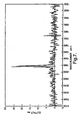
- Modelling indicates that for the structure 14 shown in figure 5b, with the dimensions indicated in table 2, the absorption coefficient along the laser is only -0.0037/m x 10 -6 , compared with -0.06/m x 10 -6 in the structure 13 of figure 5a. Fabrication of this structure has allowed the first demonstration of an electrically pumped laser in InSb at a temperature of 77K, see the output spectrum in figure 7. Previously, devices required cooling to substantially lower temperatures and/or the use of high magnetic fields.
- the phrase "action region” or “active layer” shall be taken to mean that region of the device in which substantial regeneration or recombination of carriers occurs.
- the phrase “active region” or “active layer” shall be taken to refer to the region contacted by the excluding or extracting junction, in which the exclusion or extraction occurs i.e. the region in which there is a significant change in carrier concentration.
Landscapes
- Led Devices (AREA)
- Semiconductor Lasers (AREA)
- Electrodes Of Semiconductors (AREA)
Applications Claiming Priority (3)
| Application Number | Priority Date | Filing Date | Title |
|---|---|---|---|
| GB9524414 | 1995-11-29 | ||
| GBGB9524414.1A GB9524414D0 (en) | 1995-11-29 | 1995-11-29 | Low resistance contact semiconductor device |
| PCT/GB1996/002914 WO1997020353A1 (en) | 1995-11-29 | 1996-11-27 | Low resistance contact semiconductor diode |
Publications (2)
| Publication Number | Publication Date |
|---|---|
| EP0864180A1 EP0864180A1 (en) | 1998-09-16 |
| EP0864180B1 true EP0864180B1 (en) | 2004-07-21 |
Family
ID=10784642
Family Applications (1)
| Application Number | Title | Priority Date | Filing Date |
|---|---|---|---|
| EP96939228A Expired - Lifetime EP0864180B1 (en) | 1995-11-29 | 1996-11-27 | Low resistance contact semiconductor diode |
Country Status (10)
| Country | Link |
|---|---|
| US (2) | US6133590A (enExample) |
| EP (1) | EP0864180B1 (enExample) |
| JP (1) | JP2000501238A (enExample) |
| KR (1) | KR19990071863A (enExample) |
| AU (1) | AU721907B2 (enExample) |
| CA (1) | CA2238952C (enExample) |
| DE (1) | DE69632961T2 (enExample) |
| GB (2) | GB9524414D0 (enExample) |
| RU (1) | RU2166222C2 (enExample) |
| WO (1) | WO1997020353A1 (enExample) |
Cited By (2)
| Publication number | Priority date | Publication date | Assignee | Title |
|---|---|---|---|---|
| DE102004047313B3 (de) * | 2004-09-29 | 2006-03-30 | Siced Electronics Development Gmbh & Co. Kg | Halbleiteranordnung mit einem Tunnelkontakt und Verfahren zu deren Herstellung |
| US20210184434A1 (en) * | 2018-08-24 | 2021-06-17 | Sony Semiconductor Solutions Corporation | Light-emitting device |
Families Citing this family (36)
| Publication number | Priority date | Publication date | Assignee | Title |
|---|---|---|---|---|
| ES2011531A6 (es) * | 1987-12-10 | 1990-01-16 | Poyer Michael | Dispositivo de seguridad para aparatos grabadores o reproductores de cassettes de video. |
| DE19703612A1 (de) * | 1997-01-31 | 1998-08-06 | Siemens Ag | Halbleiterlaser-Bauelement |
| US5936266A (en) * | 1997-07-22 | 1999-08-10 | The Board Of Trustees Of The University Of Illinois | Semiconductor devices and methods with tunnel contact hole sources |
| GB0012925D0 (en) | 2000-05-30 | 2000-07-19 | Secr Defence | Bipolar transistor |
| DE10057698A1 (de) * | 2000-11-21 | 2002-06-06 | Osram Opto Semiconductors Gmbh | Übereinander gestapelte Halbleiter-Diodenlaser |
| US7065124B2 (en) | 2000-11-28 | 2006-06-20 | Finlsar Corporation | Electron affinity engineered VCSELs |
| US6905900B1 (en) | 2000-11-28 | 2005-06-14 | Finisar Corporation | Versatile method and system for single mode VCSELs |
| GB0030204D0 (en) * | 2000-12-12 | 2001-01-24 | Secr Defence | Reduced noise semiconductor photodetector |
| RU2200358C1 (ru) * | 2001-06-05 | 2003-03-10 | Хан Владимир Александрович | Полупроводниковый излучающий диод |
| JP2003086898A (ja) * | 2001-09-07 | 2003-03-20 | Nec Corp | 窒化ガリウム系半導体レーザ |
| US6965626B2 (en) | 2002-09-03 | 2005-11-15 | Finisar Corporation | Single mode VCSEL |
| US6813293B2 (en) | 2002-11-21 | 2004-11-02 | Finisar Corporation | Long wavelength VCSEL with tunnel junction, and implant |
| US7170097B2 (en) * | 2003-02-14 | 2007-01-30 | Cree, Inc. | Inverted light emitting diode on conductive substrate |
| US7298942B2 (en) | 2003-06-06 | 2007-11-20 | Finisar Corporation | Pluggable optical optic system having a lens fiber stop |
| US7433381B2 (en) | 2003-06-25 | 2008-10-07 | Finisar Corporation | InP based long wavelength VCSEL |
| US7560750B2 (en) * | 2003-06-26 | 2009-07-14 | Kyocera Corporation | Solar cell device |
| US7277461B2 (en) | 2003-06-27 | 2007-10-02 | Finisar Corporation | Dielectric VCSEL gain guide |
| US7054345B2 (en) | 2003-06-27 | 2006-05-30 | Finisar Corporation | Enhanced lateral oxidation |
| US7075962B2 (en) | 2003-06-27 | 2006-07-11 | Finisar Corporation | VCSEL having thermal management |
| US6961489B2 (en) | 2003-06-30 | 2005-11-01 | Finisar Corporation | High speed optical system |
| US7149383B2 (en) | 2003-06-30 | 2006-12-12 | Finisar Corporation | Optical system with reduced back reflection |
| US7210857B2 (en) | 2003-07-16 | 2007-05-01 | Finisar Corporation | Optical coupling system |
| US6887801B2 (en) | 2003-07-18 | 2005-05-03 | Finisar Corporation | Edge bead control method and apparatus |
| US7019330B2 (en) * | 2003-08-28 | 2006-03-28 | Lumileds Lighting U.S., Llc | Resonant cavity light emitting device |
| US7031363B2 (en) | 2003-10-29 | 2006-04-18 | Finisar Corporation | Long wavelength VCSEL device processing |
| US7274040B2 (en) * | 2004-10-06 | 2007-09-25 | Philips Lumileds Lighting Company, Llc | Contact and omnidirectional reflective mirror for flip chipped light emitting devices |
| JP2006313773A (ja) * | 2005-05-06 | 2006-11-16 | Sumitomo Electric Ind Ltd | 半導体装置およびその製造方法 |
| US7535034B2 (en) | 2006-02-27 | 2009-05-19 | The Board Of Trustees Of The University Of Illinois | PNP light emitting transistor and method |
| WO2009051664A2 (en) | 2007-10-12 | 2009-04-23 | The Board Of Trustees Of The University Of Illinois | Light emitting and lasing semiconductor devices and methods |
| US7813396B2 (en) | 2007-10-12 | 2010-10-12 | The Board Of Trustees Of The University Of Illinois | Transistor laser devices and methods |
| TWI427824B (zh) * | 2008-03-14 | 2014-02-21 | 旭化成電子材料元件股份有限公司 | 紅外線發光元件 |
| JP5093063B2 (ja) | 2008-11-11 | 2012-12-05 | 住友電気工業株式会社 | 集積化半導体光素子及び半導体光装置 |
| US8502191B2 (en) | 2009-05-12 | 2013-08-06 | University Of Tsukuba | Semiconductor device, manufacturing method therefor, and solar cell |
| GB201000756D0 (en) | 2010-01-18 | 2010-03-03 | Gas Sensing Solutions Ltd | Gas sensor with radiation guide |
| GB201018417D0 (en) | 2010-11-01 | 2010-12-15 | Gas Sensing Solutions Ltd | Apparatus and method for generating light pulses from LEDs in optical absorption gas sensors |
| GB201018418D0 (en) | 2010-11-01 | 2010-12-15 | Gas Sensing Solutions Ltd | Temperature calibration methods and apparatus for optical absorption gas sensors, and optical absorption gas sensors thereby calibrated |
Family Cites Families (5)
| Publication number | Priority date | Publication date | Assignee | Title |
|---|---|---|---|---|
| FR2614135B1 (fr) * | 1987-04-14 | 1989-06-30 | Telecommunications Sa | Photodiode hgcdte a reponse rapide |
| GB9100351D0 (en) * | 1991-01-08 | 1991-02-20 | Secr Defence | Semiconductor heterostructure device |
| US5166761A (en) * | 1991-04-01 | 1992-11-24 | Midwest Research Institute | Tunnel junction multiple wavelength light-emitting diodes |
| US5338944A (en) * | 1993-09-22 | 1994-08-16 | Cree Research, Inc. | Blue light-emitting diode with degenerate junction structure |
| US5892784A (en) * | 1994-10-27 | 1999-04-06 | Hewlett-Packard Company | N-drive p-common surface emitting laser fabricated on n+ substrate |
-
1995
- 1995-11-29 GB GBGB9524414.1A patent/GB9524414D0/en active Pending
-
1996
- 1996-11-27 DE DE69632961T patent/DE69632961T2/de not_active Expired - Lifetime
- 1996-11-27 EP EP96939228A patent/EP0864180B1/en not_active Expired - Lifetime
- 1996-11-27 RU RU98112013/28A patent/RU2166222C2/ru active
- 1996-11-27 US US09/068,943 patent/US6133590A/en not_active Expired - Lifetime
- 1996-11-27 AU AU76360/96A patent/AU721907B2/en not_active Expired
- 1996-11-27 WO PCT/GB1996/002914 patent/WO1997020353A1/en not_active Ceased
- 1996-11-27 CA CA002238952A patent/CA2238952C/en not_active Expired - Lifetime
- 1996-11-27 KR KR1019980704147A patent/KR19990071863A/ko not_active Abandoned
- 1996-11-27 JP JP9520270A patent/JP2000501238A/ja active Pending
- 1996-11-27 GB GB9810627A patent/GB2321783B/en not_active Expired - Fee Related
-
2000
- 2000-08-11 US US09/636,741 patent/US6455879B1/en not_active Expired - Fee Related
Cited By (2)
| Publication number | Priority date | Publication date | Assignee | Title |
|---|---|---|---|---|
| DE102004047313B3 (de) * | 2004-09-29 | 2006-03-30 | Siced Electronics Development Gmbh & Co. Kg | Halbleiteranordnung mit einem Tunnelkontakt und Verfahren zu deren Herstellung |
| US20210184434A1 (en) * | 2018-08-24 | 2021-06-17 | Sony Semiconductor Solutions Corporation | Light-emitting device |
Also Published As
| Publication number | Publication date |
|---|---|
| GB2321783A (en) | 1998-08-05 |
| GB2321783B (en) | 2000-10-18 |
| RU2166222C2 (ru) | 2001-04-27 |
| JP2000501238A (ja) | 2000-02-02 |
| AU721907B2 (en) | 2000-07-20 |
| US6133590A (en) | 2000-10-17 |
| DE69632961D1 (de) | 2004-08-26 |
| AU7636096A (en) | 1997-06-19 |
| CA2238952C (en) | 2004-05-25 |
| GB9524414D0 (en) | 1996-01-31 |
| KR19990071863A (ko) | 1999-09-27 |
| GB9810627D0 (en) | 1998-07-15 |
| DE69632961T2 (de) | 2005-08-25 |
| EP0864180A1 (en) | 1998-09-16 |
| CA2238952A1 (en) | 1997-06-05 |
| WO1997020353A1 (en) | 1997-06-05 |
| US6455879B1 (en) | 2002-09-24 |
Similar Documents
| Publication | Publication Date | Title |
|---|---|---|
| EP0864180B1 (en) | Low resistance contact semiconductor diode | |
| US6455870B1 (en) | Unipolar light emitting devices based on III-nitride semiconductor superlattices | |
| KR101319512B1 (ko) | 질화물계 반도체 소자 및 그 제조방법 | |
| EP0446764B1 (en) | Quaternary II-VI semiconductor material for photonic device | |
| US8890177B2 (en) | Semiconductor devices made from crystalline materials with locally modifying electronic and optoelectronic properties | |
| JPH11251684A (ja) | 窒化物半導体素子 | |
| US20180374699A1 (en) | Iii-nitride tunnel junction with modified p-n interface | |
| EP0605051A1 (en) | Blue-green injection laser structure | |
| EP0284031A2 (en) | Opto-electronic device | |
| US4441187A (en) | A semiconductor laser light source | |
| US12538612B2 (en) | Light-emitting diode element | |
| US6987286B2 (en) | Yellow-green epitaxial transparent substrate-LEDs and lasers based on a strained-InGaP quantum well grown on an indirect bandgap substrate | |
| WO2001050558A1 (en) | Group iii-nitride semiconductor structures with reduced phase separation | |
| US7103080B2 (en) | Laser diode with a low absorption diode junction | |
| US6178190B1 (en) | II-VI compound semiconductor light emitting device | |
| WO2024066412A1 (zh) | 红外发光二极管及其制造方法 | |
| JPH0834338B2 (ja) | 半導体レーザ | |
| JPH09172197A (ja) | 半導体発光素子 | |
| US5084748A (en) | Semiconductor optical memory having a low switching voltage | |
| JPS61228684A (ja) | 半導体発光素子 | |
| EP0427003A1 (en) | Semiconductor light-emitting element and its manufacturing method | |
| Salii et al. | Light-Emitting AlGaAs/GaAs Diodes Based on InGaAs Strain-Compensated Quantum Wells with Minimized Internal Losses Caused by 940-nm Radiation Absorption | |
| Chung et al. | Prospects of fabricating blue/green lasers using ZnSe based metal-insulator-semiconductor (MIS) heterostructures | |
| JP2862726B2 (ja) | 半導体発光素子 | |
| JP3279226B2 (ja) | Iii族窒化物半導体発光素子 |
Legal Events
| Date | Code | Title | Description |
|---|---|---|---|
| PUAI | Public reference made under article 153(3) epc to a published international application that has entered the european phase |
Free format text: ORIGINAL CODE: 0009012 |
|
| 17P | Request for examination filed |
Effective date: 19980526 |
|
| AK | Designated contracting states |
Kind code of ref document: A1 Designated state(s): DE ES FR GB IT NL SE |
|
| 17Q | First examination report despatched |
Effective date: 20010522 |
|
| RAP1 | Party data changed (applicant data changed or rights of an application transferred) |
Owner name: QINETIQ LIMITED |
|
| GRAP | Despatch of communication of intention to grant a patent |
Free format text: ORIGINAL CODE: EPIDOSNIGR1 |
|
| GRAS | Grant fee paid |
Free format text: ORIGINAL CODE: EPIDOSNIGR3 |
|
| GRAA | (expected) grant |
Free format text: ORIGINAL CODE: 0009210 |
|
| AK | Designated contracting states |
Kind code of ref document: B1 Designated state(s): DE ES FR GB IT NL SE |
|
| PG25 | Lapsed in a contracting state [announced via postgrant information from national office to epo] |
Ref country code: NL Free format text: LAPSE BECAUSE OF FAILURE TO SUBMIT A TRANSLATION OF THE DESCRIPTION OR TO PAY THE FEE WITHIN THE PRESCRIBED TIME-LIMIT Effective date: 20040721 Ref country code: IT Free format text: LAPSE BECAUSE OF FAILURE TO SUBMIT A TRANSLATION OF THE DESCRIPTION OR TO PAY THE FEE WITHIN THE PRE;WARNING: LAPSES OF ITALIAN PATENTS WITH EFFECTIVE DATE BEFORE 2007 MAY HAVE OCCURRED AT ANY TIME BEFORE 2007. THE CORRECT EFFECTIVE DATE MAY BE DIFFERENT FROM THE ONE RECORDED.SCRIBED TIME-LIMIT Effective date: 20040721 |
|
| REG | Reference to a national code |
Ref country code: GB Ref legal event code: FG4D |
|
| REF | Corresponds to: |
Ref document number: 69632961 Country of ref document: DE Date of ref document: 20040826 Kind code of ref document: P |
|
| PG25 | Lapsed in a contracting state [announced via postgrant information from national office to epo] |
Ref country code: SE Free format text: LAPSE BECAUSE OF FAILURE TO SUBMIT A TRANSLATION OF THE DESCRIPTION OR TO PAY THE FEE WITHIN THE PRESCRIBED TIME-LIMIT Effective date: 20041021 |
|
| PG25 | Lapsed in a contracting state [announced via postgrant information from national office to epo] |
Ref country code: ES Free format text: LAPSE BECAUSE OF FAILURE TO SUBMIT A TRANSLATION OF THE DESCRIPTION OR TO PAY THE FEE WITHIN THE PRESCRIBED TIME-LIMIT Effective date: 20041101 |
|
| NLV1 | Nl: lapsed or annulled due to failure to fulfill the requirements of art. 29p and 29m of the patents act | ||
| ET | Fr: translation filed | ||
| PLBE | No opposition filed within time limit |
Free format text: ORIGINAL CODE: 0009261 |
|
| STAA | Information on the status of an ep patent application or granted ep patent |
Free format text: STATUS: NO OPPOSITION FILED WITHIN TIME LIMIT |
|
| 26N | No opposition filed |
Effective date: 20050422 |
|
| REG | Reference to a national code |
Ref country code: DE Ref legal event code: R082 Ref document number: 69632961 Country of ref document: DE Representative=s name: BEETZ & PARTNER MBB PATENT- UND RECHTSANWAELTE, DE Ref country code: DE Ref legal event code: R082 Ref document number: 69632961 Country of ref document: DE Representative=s name: BEETZ & PARTNER MBB PATENTANWAELTE, DE Ref country code: DE Ref legal event code: R082 Ref document number: 69632961 Country of ref document: DE Representative=s name: BEETZ & PARTNER MBB, DE Ref country code: DE Ref legal event code: R081 Ref document number: 69632961 Country of ref document: DE Owner name: FLIR SYSTEMS TRADING BELGIUM, BE Free format text: FORMER OWNER: QINETIQ LTD., LONDON, GB |
|
| REG | Reference to a national code |
Ref country code: FR Ref legal event code: PLFP Year of fee payment: 20 |
|
| PGFP | Annual fee paid to national office [announced via postgrant information from national office to epo] |
Ref country code: GB Payment date: 20151127 Year of fee payment: 20 Ref country code: DE Payment date: 20151127 Year of fee payment: 20 |
|
| REG | Reference to a national code |
Ref country code: GB Ref legal event code: 732E Free format text: REGISTERED BETWEEN 20160107 AND 20160113 |
|
| REG | Reference to a national code |
Ref country code: FR Ref legal event code: TP Owner name: FLIR SYSTEMS TRADING BELGIUM, BE Effective date: 20160108 |
|
| PGFP | Annual fee paid to national office [announced via postgrant information from national office to epo] |
Ref country code: FR Payment date: 20151117 Year of fee payment: 20 |
|
| REG | Reference to a national code |
Ref country code: DE Ref legal event code: R071 Ref document number: 69632961 Country of ref document: DE |
|
| REG | Reference to a national code |
Ref country code: GB Ref legal event code: PE20 Expiry date: 20161126 |
|
| PG25 | Lapsed in a contracting state [announced via postgrant information from national office to epo] |
Ref country code: GB Free format text: LAPSE BECAUSE OF EXPIRATION OF PROTECTION Effective date: 20161126 |