This invention relates to the generation of graphic data.
Heretofore, data in a frame memory are read out according to the sync
signal of a display device such as CRT in a system provided with a frame
memory such as personal computer and television game machine which is
typical of the entertainment system. In the case that an image is drawn for
each frame to display a dynamic image, usually the double buffer system in
which a frame memory is divided into a display region and drawing region is
used.
In the case of double buffer system, a display region and drawing
region are switched synchronously with the vertical retrace line erasing
period. An image of the next frame is drawn on a drawing region while an
image of a frame drawn on the display region is being displayed, and a
smooth dynamic image is thereby displayed.
However, in the case that a dynamic image is displayed using the
double buffer system, the memory use increases if drawing resolution is
enhanced because a display region and drawing region have the same size.
In addition, fine drawing finer than the display resolution can not be
realized.
Further, it is impossible to draw an image using information required
for display pixels as drawing pixels.
The graphic data generation device described in claim 1 comprises a
memory having the first memory region for storing the first graphic data
corresponding a prescribed image and the second memory region for storing
the second graphic data obtained by reducing the first graphic data, and a
graphic data generation circuit for generating the second
graphic data for display by performing reduction processing
on the first graphic data read out from the first memory region
of the memory.
The graphic data display system described in claim
7 is provided with a graphic data generation circuit for
generating the first graphic data by performing texture
mapping processing based on polygon data, a graphic data
generation circuit for generating the second graphic data by
performing reduction processing on the first graphic data,
a memory for storing the second graphic data, and a display
device for displaying the second graphic data stored in the
memory.
The graphic data generation method described in
claim 9 comprises a step (a) for generating the first graphic
data corresponding to a prescribed image by performing texture
mapping processing based on polygon data, and a step (b) for
generating the second graphic data for display by performing
reduction processing on the first graphic data.
According to the graphic data generation device
described in claim 1, the memory is provided with the first
memory region which stores the first graphic data
corresponding to a prescribed image and the second memory
region which stores the second graphic data obtained by
reducing the first graphic data, and a graphic data generation
circuit generates the second graphic data for display by performing reduction
processing on the first graphic data read out from the first memory region of
the memory.
According to the graphic data display system described in claim 7, the
graphic data generation circuit generates the first graphic data by performing
texture mapping processing based on polygon data, the graphic data generation
circuit generates the second graphic data by performing reduction processing
on the first graphic data, the memory stores the second graphic data, and the
display means displays the second graphic data stored in the memory.
According to the graphic data generation method described in claim 9,
the first graphic data corresponding to a prescribed image is generated by
performing texture mapping processing based on polygon data, and the second
graphic data for display is generated by performing reduction processing on
the first graphic data.
A preferred form of implementation of the invention described
hereinbelow seeks to reduce frame memory use without deterioration of image
quality using a frame memory of a limited capacity in the case that a dynamic
image is displayed using a double buffer system.
The preferred form of implementation of the invention provides a
method and system for generating graphic data, and more particularly a
method and system for generating graphic data which are capable of operating
with reduced memory use during using of a double buffer without
deterioration of image quality by way of applying over-sampling of high
resolution image to reduce the image.
Preferably, the graphic data generation circuit performs reduction
processing by way of over-sampling on the first graphic data corresponding
to a prescribed image in order to obtain the second graphic data, whereby
resolution of the image comprising the first graphic data is enhanced,
maintaining the memory capacity minimized, and the display resolution of the
second graphic data is enhanced.
Further, each pixel which constitutes the second graphic data is
preferably the average pixel value of adjacent four pixels in the first graphic
data, whereby, for example, a 16 bit direct color image is changed
equivalently to a 24 bit full color image.
The invention will now be further described, by way of illustrative and
non-limiting example, with reference to the accompanying drawings, in which:
Fig. 1 is a plan view illustrating one example of a home entertainment
system to which an information processing unit embodying the present
invention is applied.
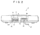
Fig. 2 is a front view of the home entertainment system 1 shown in
Fig. 1.
Fig. 3 is a side view of the home entertainment system 1 shown in Fig.
1.
Fig. 4 is a plan view for illustrating one example of a CD-ROM played
back on the home entertainment system 1 shown in Fig. 1.
Fig. 5 is a block diagram for illustrating an exemplary internal
electrical structure of the home
entertainment system 1 shown in Fig. 1.
Fig. 6 is a block diagram for illustrating an
exemplary structure of a GPU 49.
Fig. 7 is a diagram for describing procedures for
drawing a triangle.
Fig. 8 is a diagram for illustrating an exemplary
pixel format of an image stored in the drawing region of the
frame memory 58.
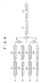
Fig. 9 is a block diagram for illustrating an
exemplary built-in average value output circuit in the TM 93
shown in Fig. 6.
Fig. 10 is a block diagram for illustrating an
exemplary built-in alpha value output circuit in the TM 93
shown in Fig. 6.
Fig. 11 is a flow chart for describing the sequence
in Bi-linear texture mapping.
Fig. 12 is a diagram for describing an exemplary
region set in the frame memory 58.
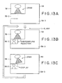
Fig. 13A is a diagram for illustrating the drawing
of a polygon image in the drawing region.
Fig. 13B is a diagram for illustrating the
arrangement in the display region of the display.polygon
graphic data obtained by over-sampling the polygon image
stored in the drawing region.
Fig. 13C is a diagram for illustrating the drawing
of a new polygon image in the drawing region and the reading
for displaying of the polygon image stored in the display
region.
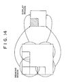
Fig. 14 is a diagram for describing the operation
of Bi-linear texture mapping.
Figs. 1 to 3 show an example of a home entertainment
system to which the present invention is applied. The home
entertainment system shown in these drawings comprises an
entertainment system body 2, an operation device 17 and
recording device 38 connectable to the entertainment system
body 2.
The entertainment system body 2 is formed in an
approximately rectangular shape as shown in Figs. 1 to 3. At
the center of the body, the body is provided with a disk support
section 3 for supporting a CD-ROM 40 (a disk equivalent to
game medium) that is a sort of the optical disk as shown in
Fig. 4, a reset switch 4 for resetting desirably a game in
running at the desired position on the entertainment system
body 2, a power switch 5 for on-off switching of a power source,
a disk operation switch 6 for operating disk placement, an
operation device 17 for operating so-called game operation,
and connection sections 7A and 7B for connecting a recording
device 38 for recording so-called game setting.
The connection sections 7A and 7B are formed in two
steps as shown in Figs. 2 and 3. On each upper step of the
connection sections 7A and 7B, a recording insertion section
8 is provided respectively for connecting the recording device
38 to the entertainment system body 2. On each lower step of
the connection sections 7A and 7B, a connection terminal
insertion sections 12 is provided respectively for connecting
the operation device 17 to the entertainment system body 2.
The recording insertion section 8 has an insertion
hole having a horizontally long rectangular shape, and memory
connection terminal section (not shown in the drawing) into
which the recording device is inserted. As shown in Fig. 2,
the recording insertion section 8 is provided with a shutter
9 for protecting the memory connection terminal section from
becoming dusty while the recording device is disconnected.
The recording device 38 has a ROM which is writable
electrically. The data which is related to so-called game is
recorded on the ROM.
In the case that the recording device 38 is mounted
on the entertainment system body 2, a user pushes the shutter
with the end of the recording device 38 inward, and inserts
the recording device 38 into the insertion hole to connect
to the memory connection terminal section to complete the
mounting work.
The connection terminal insertion section 12 has an
insertion hole having a horizontally long rectangular shape
and connection terminal 12A for connecting the connection
terminal section 26 of the operation device 17 as shown in
Fig. 2.
The operation device 17 is structured so that a user
can hold the operation device 17 with both palms and operate
desirably by free ten fingers as shown in Fig. 1. Further,
the operation device 17 is provided with operation sections
18 and 19 disposed in bilaterally symmetrical relation, a
select switch 22 and start switch 23 located on the middle
between operation sections 18 and 19, connection terminal
section 26 for connecting the entertainment system body 2 to
the operation device 17, and cable 27.
Fig. 5 shows one example of an internal electrical
structure of the above-mentioned entertainment system body
2.
The entertainment system body 2 has total two buses
of the main buss 41 and sub-buss 42. These buses are connected
to the entertainment system body 2 through SBUSIF (sub bus
interface) 43.
The main bus 41 is connected to a main CPU (Central
Processing Unit) 44 comprising a micro-processor (not shown
in the drawing) and first vector processing engine (VPE0),
main memory 45 comprising a RAM (Random Access Memory), main
direct memory access controller (main DMAC (Direct Memory
Access Controller) 46, MPEG (Moving Picture Experts Group)
decoder (MDEC) 47, second vector processing engine (VPE1) 48,
and graphical processing unit (GPU) 49 through a GPUIF
(graphical processing unit interface) 72. The GPU 49 is
provided with a PDC (Programmable display controller) 84.
On the other hand, the sub-bus 42 is connected to
a sub-CPU 50 comprising a micro-processor (not shown in the
drawing), sub-memory 51 comprising a RAM, sub-DMAC 52, ROM
53 in which programs such as operating systems are stored,
sound processing unit (SPU) 54, communication control section
(ATM) 55, CD-ROM drive 56 which is served also as a disk support
section 3, and input section 57. The operation device 17 is
connected to the connection terminal 12A of the input section
57.
The main bus 41 and sub bus 42 are connected by the
SBUSIF 43. The data from the main bus 41 is outputted to the
sub-bus 42 through the SBUSIF 43, and also the data from the
sub-bus 42 is outputted to the main bus 41 through the SBUSIF
43.
The main CPU 44 reads a start program from the ROM
53 connected to the sub-bus 42 through the SBUSIF 43 when the
entertainment system body 2 is activated, executes the start
program, and operates the operating system.
The main CPU 44 controls the CD-ROM drive 56, reads
application programs data, and sound, image, and parameter
data from the CD-ROM 40 set on the CD-ROM drive 56, and stores
these data in the main memory 45.
The main CPU 44 generates non-regular processing
data (polygon definition information) collaboratively with
the first vector processing engine (VPEO) 71 in response to
the three dimensional object data (coordinate value of the
vertex of a polygon (representative point)) comprising a
plurality of fundamental figures read from the CD-ROM 40. The
first vector processing engine (VPEO) 71 has a plurality of
operational elements for arithmetically operating real
numbers of floating point, and performs floating point
operation in parallel.
In detail, the main CPU 44 and first vector
processing engine 71 perform processing which requires fine
operation in polygon unit, that is one of the geometry
processing, for example, processing to generate data of
polygons for describing swinging of leaves with wind or rain
drop on a front window of a car. Then, the main CPU 44 and
first vector processing engine 71 supply the polygon
definition information such as the vertex information of the
three-dimensional object obtained by arithmetical operation
and shading mode information by way of packet to the main memory
45 through the main bus 41.
A polygon definition information comprises a
drawing region setting information and polygon information.
The drawing region setting information comprises an offset
coordinate in the frame buffer address of the drawing region
and an drawing clipping region coordinate. The drawing
clipping region coordinate is served to cancel drawing when
the coordinate of a polygon is located outside the drawing
region. A polygon information comprises a polygon attribute
information and vertex information. The polygon attribute
information is an information for specifying shading mode,
a blending mode, and texture mapping mode. The vertex
information is an information for specifying coordinate in
the vertex drawing region, coordinate in vertex texture region,
and vertex color.
On the other hand, the second vector processing
engine (VPE1) 48 has a plurality of operational elements for
operating real numbers of floating points like the case of
the first vector processing engine 71, and performs floating
point operation in parallel. The second vector processing
engine (VPE1) 48 generates the data from which an image is
generated by operation of the operation device 17 by a user
and processing by the matrix circuit, namely the data (polygon
definition information) for relatively simple processing
(regular processing) which is not so complicated as is
programmed by means of the second vector processing engine
48 (VPE1). For example, the second vector processing engine
48 (VPE1) performs processing such as perspective projection
conversion, parallel light source calculation, and two-dimensional
curved surface generation of a simple shape of
a body such as a building and car, and supplies the polygon
definition information generated by these processing to the
GPUIF 72.
The GPUIF 72 supplies the polygon definition
information supplied from the main CPU 44 from the main memory
45 through the main bus 41 and the polygon definition
information supplied from the second vector processing engine
48 to the GPU 49 with arbitrating between two polygon
definition information items so that these information items
does not collide each other.
The GPU 49 draws an image (referred to simply as
"polygon image" hereinafter) which represents the three
dimension using the polygon on the frame memory 58 based on
the polygon definition information supplied trough the GPUIF
72. The GPU 49 can use the frame memory 58 as a texture memory.
Therefore, the GPU 49 can perform texture mapping by placing
a pixel image on the frame memory as a texture on the polygon.
The main DMAC 46 performs control of, for example,
DMA transfer of respective circuits connected to the main bus
41. The main DMAC 46 also controls DMA transfer of respective
circuits connected to the sub-bus 42. The MDEC 47 operates
in parallel with the main CPU 44, and expands data which were
compressed using MPEG system or JPEG (Joint Photographic
Experts Group) system.
The sub-CPU 50 operates various operations
according to programs stored in the ROM 53. The sub-DMAC 52
controls DMA transfer of respective circuits connected to the
sub-bus 42 only while the SBUSIF 43 disconnects the sub-bus
42 from the main bus 41.
The SPU 54 reads sound data from the sound memory
59 in response to a sound command supplied from the sub-CPU
50 or sub-DMAC 52, and outputs it as an audio output from a
speaker 202 through driver 201.
The communication control section (ATM) 55 is
connected to the public lines, and transmits/receives data
through the lines.
The input section 57 has a connection terminal
section 12 A for connecting the operation device 17, video
input circuit 82 for receiving video data from other devices
(not shown in the drawing), and audio input circuit 83 for
receiving audio data from other devices (not shown in the
drawing).
Fig. 6 is a block diagram for illustrating an
exemplary structure of the GPU 49. The Pre Processor (PP) 91
performs pre-processing for performing polygon drawing such
as generation of various parameters. Herein, the various
parameters means parameters for setting in the DDA (Digital
Differential Analyzer) 92 described hereinafter and
parameters for specifying operation mode, namely Alpha
Blending ON/OFF, Texture Modulate ON/OFF, of the texture
mapping section (TM Texture Mapping)) 93 served as a graphic
data generation device.
The DDA 92 comprises an accumulator and generates
pixel information. The TM 93 performs texture mapping
processing. The memory interface (MEMIF) 94 performs
interface processing for taking an access to the frame memory
58.
The frame memory 58 is used as a frame memory and
texture memory, and stores the polygon drawing data and texture
data. The texture data stored in the frame memory 58 are read
as desired by the texture mapping section 93, and the read
texture data is used for placing it on a polygon.
PDC 84 reads the drawing data stored in the frame
memory 58 through the MEMIF 94, and outputs the read drawing
data as the digital video data of two series. The Digital to
Analog converter (DAC) 96 converts the one series of video
data from the PDC 84 to an analog video signal, and output
it. A display device 200 such as a CRT or LCD is connected
to the PDC 84.
An example in which a triangle is drawn is described
with reference to Fig. 7. Fig. 7 shows the drawing region 58-1
(refer to Fig. 12) of the frame memory 58, coordinates of the
upper left corner, upper right corner, lower left corner, and
lower right corner are respectively (0,0), (1280,0), (0,960),
and (1280,960), wherein the unit is a pixel. As shown in Fig.
7, in the case that a triangle having vertexes A0 (XA0, YA0),
BO (XB0, YB0), and CO (XC0, YC0) is drawn, first the respective
coordinates of vertexes A0, B0, and C0 are given to the PP
91 as input data. The vertex which is located in the left (in
this example, vertex A0) out of top vertexes on the screen
is used as the starting vertex. The vertex which is located
in the left out of vertexes excepting the starting vertex (in
this example, vertex B0) is assigned as the second vertex,
and the residual vertex (in this example, C0) is assigned as
the third vertex. When, the PP 91 calculates the gradient "a"
of the line drawn from the starting vertex to the second vertex
(displacement of x-coordinate when y-coordinate is displaced
by 1), a gradient "b" of the line drawn from the starting vertex
to the third vertex, and a gradient "c" of the line drawn from
the second vertex to third vertex, and these gradient values
"a", "b", and "c" are set respectively to the DDA 92. For the
purpose of simplification herein, it is assumed that y-coordinate
of the second vertex is the same as y-coordinate
of the third vertex.
In
DDA 92, the following calculation is operated
based on the data set by means of the
PP 91. Herein DDA0 to
DDA3 are variables. The point P1 shown in Fig. 7 is the
starting point when the triangle is drawn, the point P2 is
the end point when the triangle is drawn, and the point P3
represents the pixel between the point P1 and the point P2.
The respective coordinates of the starting point P1, end point
P2, and the point P3 between the starting point P1 and end
point P2 are (DDA0, DDA3) (DDA2, DDA3), (DDA1, DDA3), variables
DDA0, DDA2, and DDA1 are horizontal x-coordinate values, and
variables DDA3 is a vertical y-coordinate value. The triangle
is drawn by repeating the step (0) and steps (1) to (4).
In the above-mentioned processing, the triangle is
drawn as described herein under. As shown in Fig. 7, "1" is
added successively to the variable DDA1 which is the horizontal
coordinate value of the point P3, and a line which is part
of the triangle is thereby drawn successively from the starting
point P1 toward the end point P2 one pixel by one pixel as
shown with a solid line arrow C. When the value of the variable
DDA1 exceeds the value of the variable DDA2 which is the value
of the end point, "1" is added to the variable DDA3 which is
the vertical coordinate value, simultaneously "a" is added
to the variable DDA0 which is the horizontal coordinate value
of the starting point P1, and "b" is added to the variable
DDA2 which is the horizontal coordinate value of the end point
P2. Hence, as shown with a dashed line arrow and solid line
arrow "a" under the starting point P1 in Fig. 7, the position
of the starting point P1 is changed, and as shown with a dashed
line arrow and solid line arrow "b" under the end point P2,
the position of the end point P2 is changed. As shown with
a solid line arrow C, a line which is part of the triangle
is drawn from the starting point P1 which is changed in position
to the end point P2 which is changed in position successively
as described herein above one pixel by one pixel.
As described herein above, in the DDA 92, coordinate
of the pixel to be drawn is calculated using the accumulator
along the raster. The DDA 92 calculates also the gradient of
vertex color similarly and coordinate in the texture space
in addition to the acquisition of drawing coordinate in order
to realize glow shading.
The above-mentioned various respective data
calculated by the DDA 92 are supplied to the TM 93. The TM
93 reads the texture data from the frame memory 58 based on
the data supplied from the DDA 92, and writes a prescribed
image (the first graphic data) on the drawing region (the first
memory region) 58-1 of the frame memory 58 through the MEMIF
94. During retrace line erasing period, regarding the entire
region of the drawing region 58-1 as the texture data,
the TM 93 reduces the image drawn thereon by way of Bi-linear
texture mapping method, which will be described hereinafter,
to generate a reduced image (second graphic data), and draws
the reduced image on the display region (second memory region)
58-2 (refer to Fig. 12).
The PDC 84 reads the graphic data of the image drawn
on the display region 58-2 of the frame memory 58 through the
MEMIF 94, and outputs the graphic data as two series of digital
video signal. One series out of two is converted to an analog
video signal in the DAC 96, and outputted on the screen of
a display 200 as an image.
Fig. 8 shows a data format of a pixel stored in the
frame memory 58. Each pixel is represented by total 16 bits
comprising bits from bit 0 to bit 15. In the first bit 0, alpha
information for indicating transparent information is
contained. In the next 5 bits (from bit 1 to bit 5), pixel
data of blue (B) component is contained. In the next 5 bits
(from bit 6 to bit 10), pixel data of green (G) component is
contained. In the final 5 bits (bit 11 to bit 15), pixel data
of red (R) component is contained.
Fig. 9 shows an example of the average value output
circuit which extracts data of a prescribed color component
of R, G, and B out of pixel data stored in the format shown
in Fig. 8 every 4 pixels and calculates the average value of
these data. Circuits as shown in Fig. 9 are provided in the
TM 93 respectively for R component, G component, and B
component.
The texture read sections 101 and 102 read the pixel
data corresponding to the red components Rl and R2 of a
prescribed pixel of the texture data stored in the drawing
region (drawing region) 58-1 (refer to Fig. 12) of the frame
memory 58 and outputs it. Further, the texture read sections
103 and 104 read the pixel data corresponding to the red
components R3 and R4 of another prescribed pixel of the texture
data from the frame memory 58 and outputs it.
The shifters 105, 106, 107, and 108 shift the texture
data supplied respectively from the texture read sections 101,
102, 103, and 104 by 3 bits in the MSB (Most Significant Bit)
direction, and then outputs them. In other words, the
shifters 105, 106, 107, and 108 convert the texture data having
5 bits to a texture data having 8 bits and output them.
The adder 109 adds the output from the shifter 105
to the output from the shifter 106. The adder 110 adds the
output from the shifter 107 to the output from the shifter
108. Further, the adder 111 adds the outputfrom.the adder
109 to the output from the adder 110.
The shifter 112 shifts the output from the adder 111
by 2 bits in the direction of the LSB (Least Significant Bit).
In other words, by performing the shift processing, the shifter
113 divides the total of respective R component pixel values
of added 4 pixels which are added by means of the adders 109
to 111 by 4 to figure out the average value. The pixel write
section (Pixel write) 113 writes the average pixel data of
8 bit R component outputted from the shifter 112 on the display
region 58-2 (Fig. 12) of the frame memory 58.
The same structure as the circuit shown in Fig. 9
is provided in the TM 93 respectively for G component and B
component. Like the processing for calculating the average
value of the pixel value of R component of the above-mentioned
four pixels, those circuits calculate respective averages of
G component and B component every 4 pixels. These average
values are written in the drawing region 58-2 of the frame
memory 58.
The alpha-value output circuit shown in Fig. 10,
provided in the TM93 shown in Fig. 6, extracts the 1 bit alpha
information for indicating the mixing ratio out of the pixel
data stored in the frame memory 58 in the format shown in Fig.
8 every adjacent 4 pixels in the drawing region 58-1 and figures
out those average values.
The texture read sections 121 and 122 read alpha
information (α1) and (α2) of the prescribed pixel stored
respectively in the drawing region 58-1 of the frame memory
58 and output them. The texture read sections 123 and 124 read
alpha information (α3) and (α4) of another prescribed pixel
stored respectively in the drawing region 58-1 and output them.
The comparators 125, 126, 127, and 128 detect
respectively whether the value of alpha information (α1), (α
2), (α3), and (α4) supplied from the texture read sections
121, 122, 123, and 124 are 0 or 1, and if the values of supplied
alpha information (α1), (α2), (α3), and (α4) are "0", then
the comparator 125, 126, 127 and 128 outputs respectively the
alpha information of 8 bits stored in the alpha register (Alpha
register 0) 129, on the other hand, if the values of alpha
information (α1), (α2), (α3), and (α4) are "1", the
respective alpha values stored in the alpha register (Alpha
Register 1) 130 are outputted.
The adder 131 adds the output of the comparator 125
to the output of the comparator 126. The adder 132 adds the
output of the comparator 127 to the output of the comparator
128. The adder 133 adds the output of the adder 131 to the
output of the adder 132.
The shifter 134 shifts the output of the adder 133
by 2 bits in the LSB direction. In detail, by performing the
shift processing, the shifter 134 divides the tbtal of alpha
values of 4 pixels added by the adder 133 by 4 to figure out
the average value. The pixel write section 135 writes the
average value (8 bits) of the alpha value outputted from the
shifter 134 on the display region 58-2 of the frame memory
58. Circuits as shown in Fig. 10 are provided in the TM 93
respectively for R component, G component, and B component.
Next, operations of the entertainment system body
2 shown in Fig. 5 are described with reference to the flow
chart in Fig. 11. In the step S1, the main CPU 44 generates
a command for initializing the frame memory 58 provided to
the GPU 49, and stores it in the main memory 45. The "command"
means a command for setting the drawing region 58-1 and display
region 58-2 in the frame memory 58 (refer to Fig. 12), and
a command for setting the offset of the coordinate and so on.
The main DMAC 46 transmits the above-mentioned commands stored
in the main memory 45 to the GPU 49 through the GPUIF 72.
In the step S2, the main DMAC 46 transmits the
texture data which is previously stored in the main memory
45 and CLUT (Color Look Up Table) data to the GPU 49 through
the GPUIF 72, and disposes them in the texture buffer 58-3
of the frame memory 58.
In the step S3, the main CPU 44 calculates the
polygon definition information comprising vertex information,
shading mode information, texture information; and vertex
color information required for drawing using the first vector
processing engine (VPEO) 71, and stores it in the main memory
45.
In the step S4, the main DMAC 46 starts transmission
processing of the polygon definition information stored on
the main memory 45 to the GPU 49 through the GPUIF 72.
In the step S5, the GPU 49 performs texture mapping
processing and starts drawing of the polygon image on the
drawing region 58 of the frame memory 58 according to the
polygon definition information transmitted through the GPUIF
72 as shown in Fig. 13A.
In the step S6, after the processing which started
in the step S4 was completed, regarding the polygon image
stored on the drawing region 58-1 as a texture, the main CPU
44 stores the polygon definition information for drawing the
image on the display region 58-2 using the polygon image data
in the main memory 45.
In the step S7, the main DMAC 46 transmits the
polygon definition information stored in the main memory 45
in these step S6 to the GPU 49 through the GPUIF 72.
In the step 8, regarding the polygon image drawn on
the drawing region 58-1 on the frame memory 58 as a texture,
the GPU 49 draws the reduced polygon image regarded as a texture
on the display region 58-2 as shown in Fig. 13B. When, the
GPU 49 performs reduction processing of the polygon image
regarded as a texture using the Bi-linear texture mapping
method described hereinafter.
As shown in Fig. 13C, the PDC 84 outputs a video
signal corresponding to the image drawn on the display region
58-2, and the video signal is displayed on a display device
200.
In the step S9, the main CPU judges whether the
above-mentioned polygon processing is completed on every
frames. If the judgement indicates that polygon processing
is completed not on every frames, the sequence returns to the
step S2, and the processing of the step S2 and after the step
S2 is performed. In the step S5, as shown in Fig. 13C, a
polygon image to be displayed in the next frame is drawn on
the drawing region 58-1. On the other hand, if the main CPU
44 judges polygon processing to have been completed on every
frames, then the processing is brought to an end.
Bi-linear texture mapping is described with
reference to Fig. 14. Fig. 14 shows an arbitrary 4×4 pixel
region on the drawing region of the frame memory 58 and a 2
×2 pixel region corresponding to the above-mentioned 4×
4 pixel region on the display region 58-2. Color resolution
of each pixel drawn on the drawing region 58-1 is 16 bit direct
color. As described hereinbefore with reference to Fig. 8,
each pixel has 16 bits comprising 5 bits respectively for R,
G, and B and 1 bit for alpha bit.
First, a pixel value represented by 5 bits of 2
×2 pixels located at the upper left corner out of the 4×
4 pixels are extracted, and these pixels are inputted to the
texture read sections 101 to 104 of the average value output
circuit shown in Fig. 9. The inputted respective pixel values
are shifted by 3 bits respectively in the MSB direction in
the shifters 105 to 108, thereby the value is multiplied by
8 to convert it to 8 bit value. These values are added by the
adders 109, 110, and 111, and shifted by 2 bits in the LSB
direction by the shifter 112, thereby the value is divided
by 4. Thereby, an average of the value that 4 pixels are
multiplied by 8 to convert it to 8 bit value is obtained.
To express the pixel value of each pixel which is
represented by the above-mentioned 16 bit direct color, the
value of R, G, and B of each pixel is changed to 8 bit value.
Finally, the value of R, G, and B of each pixel is outputted
in the form of 8 bit data respectively, and written on the
display region by the pixel write section 113.
On the other hand, alpha information items having
1 bit of the respective pixels are inputted to the texture
read sections 121 to 124 of the alpha value output circuit
shown in Fig. 10. The comparators 125 to 128 detects whether
the input alpha information is 0 or 1, and depending on the
detection result, any one of alpha values stored in the alpha
register 129 and alpha register 130 is replaced with the input
respective alpha information. The alpha value set in the
alpha registers 129 and 130 can be changed, for example, every
one polygon.
The respective alpha values of the four pixels
having replaced alpha information are added by the adders 131
to 133, and then it is divided by 4 to calculate the average
value of the respective alpha values of the four pixels
corresponding to the respective alpha information items.
The average value of the alpha value having 8 bits
is supplied to the pixel write section 135, and written on
the display region 58-2 of the frame memory 58 through the
MEMIF 94. Hence, the pixels located at the upper left corner
of the display region 58-2 shown in Fig. 14 is drawn.
Next, 4 pixels located on the right side of the
above-mentioned 4 pixels on the drawing region 58-1 is
subjected to the same processing as described herein above,
and the corresponding data are written on the display region
58-2. Similarly as described herein under, average values of
all the pixels drawn on the drawing region 58-1 are obtained
every 4 bits, and drawn on the display region 58-2 as the value
of one pixel.
The PDC 84 outputs digital video signal of two series
corresponding to each pixel based on the pixel value of each
pixel drawn on the display region 58-2 of the frame buffer
58. One series out of two series is converted to an analog
signal and then outputted as an analog video signal.
As described herein above, 16 bit direct color image
having 5 bits of R component, 5 bits of G component, 5 bits
of B component, and 1 bit of alpha information drawn on the
drawing region 58-1 is reduced to 1/2 respectively in
horizontal and vertical direction (the number of pixels are
reduced to 1/4), and is drawn on the display region 58-2 in
the form of 24 bit full color image. Because information of
4 pixels of the image drawn on the drawing region 58-1 is
reflected on each pixel of the image drawn on the display region
58-2 by the above-mentioned over-sampling, the resultant
image contains substantially the information of precision
finer than one pixel for one pixel. Therefore, it is possible
to display an image which is clear and sharp at the polygon
periphery, namely the edge, of the displayed image which is
read out from the display region and displayed by the display
device and has high resolution.
Hence, drawing resolution can be enhanced to a level
finer than display resolution, and the enhanced resolution
allows memory use to be reduced without deterioration of
drawing quality. Further, enhanced resolution leads to fine
graphical drawing regardless of display resolution. As the
result, an image of high resolution finer than the display
resolution can be displayed. Further, because a polygon image
once drawn is subjected to over-sampling and displayed, color
resolution per one drawing pixel can be reduced from that of
display pixel, therefore memory use can be reduced.
In the embodiment described herein above, a pixel
value average of 4 pixels is calculated in Bi-linear texture
sampling. However, a pixel value average of arbitrary number
of pixels may be calculated.
In the above embodiment, there showed an example of
connecting the speaker 202 via the display unit 200 and the
driver 201. These units may be constituted as an integrated
type or portable type.
The example in which the speaker 202 is connected
through the display device 200 and driver 201 has been
described, however these components may be combined or may
be structured in potable style.
Although a certain preferred embodiment of the
present invention has been shown and described in detail, it
should be understood that various changes and modifications
may be made therein without departing from the scope of the
appended claims.