EP0863497A1 - Einrichtung zur Generierung vong raphischen Daten mit Bereichen im Pufferspeicher für normale und verkleinerte grafische Daten - Google Patents
Einrichtung zur Generierung vong raphischen Daten mit Bereichen im Pufferspeicher für normale und verkleinerte grafische Daten Download PDFInfo
- Publication number
- EP0863497A1 EP0863497A1 EP98301603A EP98301603A EP0863497A1 EP 0863497 A1 EP0863497 A1 EP 0863497A1 EP 98301603 A EP98301603 A EP 98301603A EP 98301603 A EP98301603 A EP 98301603A EP 0863497 A1 EP0863497 A1 EP 0863497A1
- Authority
- EP
- European Patent Office
- Prior art keywords
- graphic data
- memory
- data
- pixel
- region
- Prior art date
- Legal status (The legal status is an assumption and is not a legal conclusion. Google has not performed a legal analysis and makes no representation as to the accuracy of the status listed.)
- Withdrawn
Links
- 239000000872 buffer Substances 0.000 title description 5
- 238000012545 processing Methods 0.000 claims abstract description 67
- 238000013507 mapping Methods 0.000 claims abstract description 20
- 238000005070 sampling Methods 0.000 claims abstract description 9
- 238000000034 method Methods 0.000 claims description 13
- 238000010586 diagram Methods 0.000 description 12
- 101001080624 Homo sapiens Proline/serine-rich coiled-coil protein 1 Proteins 0.000 description 10
- 102100027427 Proline/serine-rich coiled-coil protein 1 Human genes 0.000 description 10
- 102000012688 DDA1 Human genes 0.000 description 9
- 101150044395 dda1 gene Proteins 0.000 description 9
- 238000003780 insertion Methods 0.000 description 8
- 230000037431 insertion Effects 0.000 description 8
- 239000007853 buffer solution Substances 0.000 description 4
- 230000006866 deterioration Effects 0.000 description 3
- 238000002156 mixing Methods 0.000 description 3
- 238000012546 transfer Methods 0.000 description 3
- 238000004891 communication Methods 0.000 description 2
- 239000000284 extract Substances 0.000 description 2
- 230000004044 response Effects 0.000 description 2
- 230000005540 biological transmission Effects 0.000 description 1
- 238000006243 chemical reaction Methods 0.000 description 1
- 238000001514 detection method Methods 0.000 description 1
- 238000006073 displacement reaction Methods 0.000 description 1
- 230000010365 information processing Effects 0.000 description 1
- 239000011159 matrix material Substances 0.000 description 1
- 238000012986 modification Methods 0.000 description 1
- 230000004048 modification Effects 0.000 description 1
- 230000003287 optical effect Effects 0.000 description 1
- 238000007781 pre-processing Methods 0.000 description 1
Images


Classifications
-
- G—PHYSICS
- G09—EDUCATION; CRYPTOGRAPHY; DISPLAY; ADVERTISING; SEALS
- G09G—ARRANGEMENTS OR CIRCUITS FOR CONTROL OF INDICATING DEVICES USING STATIC MEANS TO PRESENT VARIABLE INFORMATION
- G09G5/00—Control arrangements or circuits for visual indicators common to cathode-ray tube indicators and other visual indicators
- G09G5/36—Control arrangements or circuits for visual indicators common to cathode-ray tube indicators and other visual indicators characterised by the display of a graphic pattern, e.g. using an all-points-addressable [APA] memory
- G09G5/39—Control of the bit-mapped memory
- G09G5/399—Control of the bit-mapped memory using two or more bit-mapped memories, the operations of which are switched in time, e.g. ping-pong buffers
-
- G—PHYSICS
- G09—EDUCATION; CRYPTOGRAPHY; DISPLAY; ADVERTISING; SEALS
- G09G—ARRANGEMENTS OR CIRCUITS FOR CONTROL OF INDICATING DEVICES USING STATIC MEANS TO PRESENT VARIABLE INFORMATION
- G09G5/00—Control arrangements or circuits for visual indicators common to cathode-ray tube indicators and other visual indicators
- G09G5/36—Control arrangements or circuits for visual indicators common to cathode-ray tube indicators and other visual indicators characterised by the display of a graphic pattern, e.g. using an all-points-addressable [APA] memory
- G09G5/39—Control of the bit-mapped memory
- G09G5/393—Arrangements for updating the contents of the bit-mapped memory
-
- G—PHYSICS
- G09—EDUCATION; CRYPTOGRAPHY; DISPLAY; ADVERTISING; SEALS
- G09G—ARRANGEMENTS OR CIRCUITS FOR CONTROL OF INDICATING DEVICES USING STATIC MEANS TO PRESENT VARIABLE INFORMATION
- G09G2340/00—Aspects of display data processing
- G09G2340/04—Changes in size, position or resolution of an image
- G09G2340/0407—Resolution change, inclusive of the use of different resolutions for different screen areas
Definitions
- This invention relates to the generation of graphic data.
- data in a frame memory are read out according to the sync signal of a display device such as CRT in a system provided with a frame memory such as personal computer and television game machine which is typical of the entertainment system.
- a display device such as CRT
- a frame memory such as personal computer and television game machine which is typical of the entertainment system.
- an image is drawn for each frame to display a dynamic image
- usually the double buffer system in which a frame memory is divided into a display region and drawing region is used.
- a display region and drawing region are switched synchronously with the vertical retrace line erasing period.
- An image of the next frame is drawn on a drawing region while an image of a frame drawn on the display region is being displayed, and a smooth dynamic image is thereby displayed.
- the graphic data generation device described in claim 1 comprises a memory having the first memory region for storing the first graphic data corresponding a prescribed image and the second memory region for storing the second graphic data obtained by reducing the first graphic data, and a graphic data generation circuit for generating the second graphic data for display by performing reduction processing on the first graphic data read out from the first memory region of the memory.
- the graphic data display system described in claim 7 is provided with a graphic data generation circuit for generating the first graphic data by performing texture mapping processing based on polygon data, a graphic data generation circuit for generating the second graphic data by performing reduction processing on the first graphic data, a memory for storing the second graphic data, and a display device for displaying the second graphic data stored in the memory.
- the graphic data generation method described in claim 9 comprises a step (a) for generating the first graphic data corresponding to a prescribed image by performing texture mapping processing based on polygon data, and a step (b) for generating the second graphic data for display by performing reduction processing on the first graphic data.
- the memory is provided with the first memory region which stores the first graphic data corresponding to a prescribed image and the second memory region which stores the second graphic data obtained by reducing the first graphic data, and a graphic data generation circuit generates the second graphic data for display by performing reduction processing on the first graphic data read out from the first memory region of the memory.
- the graphic data generation circuit generates the first graphic data by performing texture mapping processing based on polygon data, the graphic data generation circuit generates the second graphic data by performing reduction processing on the first graphic data, the memory stores the second graphic data, and the display means displays the second graphic data stored in the memory.
- the first graphic data corresponding to a prescribed image is generated by performing texture mapping processing based on polygon data
- the second graphic data for display is generated by performing reduction processing on the first graphic data
- a preferred form of implementation of the invention described hereinbelow seeks to reduce frame memory use without deterioration of image quality using a frame memory of a limited capacity in the case that a dynamic image is displayed using a double buffer system.
- the preferred form of implementation of the invention provides a method and system for generating graphic data, and more particularly a method and system for generating graphic data which are capable of operating with reduced memory use during using of a double buffer without deterioration of image quality by way of applying over-sampling of high resolution image to reduce the image.
- the graphic data generation circuit performs reduction processing by way of over-sampling on the first graphic data corresponding to a prescribed image in order to obtain the second graphic data, whereby resolution of the image comprising the first graphic data is enhanced, maintaining the memory capacity minimized, and the display resolution of the second graphic data is enhanced.
- each pixel which constitutes the second graphic data is preferably the average pixel value of adjacent four pixels in the first graphic data, whereby, for example, a 16 bit direct color image is changed equivalently to a 24 bit full color image.
- Fig. 1 is a plan view illustrating one example of a home entertainment system to which an information processing unit embodying the present invention is applied.
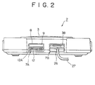
- Fig. 2 is a front view of the home entertainment system 1 shown in Fig. 1.
- Fig. 3 is a side view of the home entertainment system 1 shown in Fig. 1.
- Fig. 4 is a plan view for illustrating one example of a CD-ROM played back on the home entertainment system 1 shown in Fig. 1.
- Fig. 5 is a block diagram for illustrating an exemplary internal electrical structure of the home
- Fig. 6 is a block diagram for illustrating an exemplary structure of a GPU 49.
- Fig. 7 is a diagram for describing procedures for drawing a triangle.
- Fig. 8 is a diagram for illustrating an exemplary pixel format of an image stored in the drawing region of the frame memory 58.
- Fig. 9 is a block diagram for illustrating an exemplary built-in average value output circuit in the TM 93 shown in Fig. 6.
- Fig. 10 is a block diagram for illustrating an exemplary built-in alpha value output circuit in the TM 93 shown in Fig. 6.
- Fig. 11 is a flow chart for describing the sequence in Bi-linear texture mapping.
- Fig. 12 is a diagram for describing an exemplary region set in the frame memory 58.
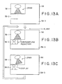
- Fig. 13A is a diagram for illustrating the drawing of a polygon image in the drawing region.
- Fig. 13B is a diagram for illustrating the arrangement in the display region of the display.polygon graphic data obtained by over-sampling the polygon image stored in the drawing region.
- Fig. 13C is a diagram for illustrating the drawing of a new polygon image in the drawing region and the reading for displaying of the polygon image stored in the display region.
- Fig. 14 is a diagram for describing the operation of Bi-linear texture mapping.
- Figs. 1 to 3 show an example of a home entertainment system to which the present invention is applied.
- the home entertainment system shown in these drawings comprises an entertainment system body 2, an operation device 17 and recording device 38 connectable to the entertainment system body 2.
- the entertainment system body 2 is formed in an approximately rectangular shape as shown in Figs. 1 to 3. At the center of the body, the body is provided with a disk support section 3 for supporting a CD-ROM 40 (a disk equivalent to game medium) that is a sort of the optical disk as shown in Fig. 4, a reset switch 4 for resetting desirably a game in running at the desired position on the entertainment system body 2, a power switch 5 for on-off switching of a power source, a disk operation switch 6 for operating disk placement, an operation device 17 for operating so-called game operation, and connection sections 7A and 7B for connecting a recording device 38 for recording so-called game setting.
- a CD-ROM 40 a disk equivalent to game medium
- a reset switch 4 for resetting desirably a game in running at the desired position on the entertainment system body 2
- a power switch 5 for on-off switching of a power source
- a disk operation switch 6 for operating disk placement
- an operation device 17 for operating so-called game operation
- connection sections 7A and 7B are formed in two steps as shown in Figs. 2 and 3.
- a recording insertion section 8 is provided respectively for connecting the recording device 38 to the entertainment system body 2.
- a connection terminal insertion sections 12 is provided respectively for connecting the operation device 17 to the entertainment system body 2.
- the recording insertion section 8 has an insertion hole having a horizontally long rectangular shape, and memory connection terminal section (not shown in the drawing) into which the recording device is inserted. As shown in Fig. 2, the recording insertion section 8 is provided with a shutter 9 for protecting the memory connection terminal section from becoming dusty while the recording device is disconnected.
- the recording device 38 has a ROM which is writable electrically. The data which is related to so-called game is recorded on the ROM.
- the recording device 38 is mounted on the entertainment system body 2
- a user pushes the shutter with the end of the recording device 38 inward, and inserts the recording device 38 into the insertion hole to connect to the memory connection terminal section to complete the mounting work.
- connection terminal insertion section 12 has an insertion hole having a horizontally long rectangular shape and connection terminal 12A for connecting the connection terminal section 26 of the operation device 17 as shown in Fig. 2.
- the operation device 17 is structured so that a user can hold the operation device 17 with both palms and operate desirably by free ten fingers as shown in Fig. 1. Further, the operation device 17 is provided with operation sections 18 and 19 disposed in bilaterally symmetrical relation, a select switch 22 and start switch 23 located on the middle between operation sections 18 and 19, connection terminal section 26 for connecting the entertainment system body 2 to the operation device 17, and cable 27.
- Fig. 5 shows one example of an internal electrical structure of the above-mentioned entertainment system body 2.
- the entertainment system body 2 has total two buses of the main buss 41 and sub-buss 42. These buses are connected to the entertainment system body 2 through SBUSIF (sub bus interface) 43.
- SBUSIF sub bus interface
- the main bus 41 is connected to a main CPU (Central Processing Unit) 44 comprising a micro-processor (not shown in the drawing) and first vector processing engine (VPE0), main memory 45 comprising a RAM (Random Access Memory), main direct memory access controller (main DMAC (Direct Memory Access Controller) 46, MPEG (Moving Picture Experts Group) decoder (MDEC) 47, second vector processing engine (VPE1) 48, and graphical processing unit (GPU) 49 through a GPUIF (graphical processing unit interface) 72.
- the GPU 49 is provided with a PDC (Programmable display controller) 84.
- the sub-bus 42 is connected to a sub-CPU 50 comprising a micro-processor (not shown in the drawing), sub-memory 51 comprising a RAM, sub-DMAC 52, ROM 53 in which programs such as operating systems are stored, sound processing unit (SPU) 54, communication control section (ATM) 55, CD-ROM drive 56 which is served also as a disk support section 3, and input section 57.
- the operation device 17 is connected to the connection terminal 12A of the input section 57.
- the main bus 41 and sub bus 42 are connected by the SBUSIF 43.
- the data from the main bus 41 is outputted to the sub-bus 42 through the SBUSIF 43, and also the data from the sub-bus 42 is outputted to the main bus 41 through the SBUSIF 43.
- the main CPU 44 reads a start program from the ROM 53 connected to the sub-bus 42 through the SBUSIF 43 when the entertainment system body 2 is activated, executes the start program, and operates the operating system.
- the main CPU 44 controls the CD-ROM drive 56, reads application programs data, and sound, image, and parameter data from the CD-ROM 40 set on the CD-ROM drive 56, and stores these data in the main memory 45.
- the main CPU 44 generates non-regular processing data (polygon definition information) collaboratively with the first vector processing engine (VPEO) 71 in response to the three dimensional object data (coordinate value of the vertex of a polygon (representative point)) comprising a plurality of fundamental figures read from the CD-ROM 40.
- the first vector processing engine (VPEO) 71 has a plurality of operational elements for arithmetically operating real numbers of floating point, and performs floating point operation in parallel.
- the main CPU 44 and first vector processing engine 71 perform processing which requires fine operation in polygon unit, that is one of the geometry processing, for example, processing to generate data of polygons for describing swinging of leaves with wind or rain drop on a front window of a car. Then, the main CPU 44 and first vector processing engine 71 supply the polygon definition information such as the vertex information of the three-dimensional object obtained by arithmetical operation and shading mode information by way of packet to the main memory 45 through the main bus 41.
- a polygon definition information comprises a drawing region setting information and polygon information.
- the drawing region setting information comprises an offset coordinate in the frame buffer address of the drawing region and an drawing clipping region coordinate.
- the drawing clipping region coordinate is served to cancel drawing when the coordinate of a polygon is located outside the drawing region.
- a polygon information comprises a polygon attribute information and vertex information.
- the polygon attribute information is an information for specifying shading mode, a blending mode, and texture mapping mode.
- the vertex information is an information for specifying coordinate in the vertex drawing region, coordinate in vertex texture region, and vertex color.
- the second vector processing engine (VPE1) 48 has a plurality of operational elements for operating real numbers of floating points like the case of the first vector processing engine 71, and performs floating point operation in parallel.
- the second vector processing engine (VPE1) 48 generates the data from which an image is generated by operation of the operation device 17 by a user and processing by the matrix circuit, namely the data (polygon definition information) for relatively simple processing (regular processing) which is not so complicated as is programmed by means of the second vector processing engine 48 (VPE1).
- the second vector processing engine 48 (VPE1) performs processing such as perspective projection conversion, parallel light source calculation, and two-dimensional curved surface generation of a simple shape of a body such as a building and car, and supplies the polygon definition information generated by these processing to the GPUIF 72.
- the GPUIF 72 supplies the polygon definition information supplied from the main CPU 44 from the main memory 45 through the main bus 41 and the polygon definition information supplied from the second vector processing engine 48 to the GPU 49 with arbitrating between two polygon definition information items so that these information items does not collide each other.
- the GPU 49 draws an image (referred to simply as "polygon image” hereinafter) which represents the three dimension using the polygon on the frame memory 58 based on the polygon definition information supplied trough the GPUIF 72.
- the GPU 49 can use the frame memory 58 as a texture memory. Therefore, the GPU 49 can perform texture mapping by placing a pixel image on the frame memory as a texture on the polygon.
- the main DMAC 46 performs control of, for example, DMA transfer of respective circuits connected to the main bus 41.
- the main DMAC 46 also controls DMA transfer of respective circuits connected to the sub-bus 42.
- the MDEC 47 operates in parallel with the main CPU 44, and expands data which were compressed using MPEG system or JPEG (Joint Photographic Experts Group) system.
- the sub-CPU 50 operates various operations according to programs stored in the ROM 53.
- the sub-DMAC 52 controls DMA transfer of respective circuits connected to the sub-bus 42 only while the SBUSIF 43 disconnects the sub-bus 42 from the main bus 41.
- the SPU 54 reads sound data from the sound memory 59 in response to a sound command supplied from the sub-CPU 50 or sub-DMAC 52, and outputs it as an audio output from a speaker 202 through driver 201.
- the communication control section (ATM) 55 is connected to the public lines, and transmits/receives data through the lines.
- the input section 57 has a connection terminal section 12 A for connecting the operation device 17, video input circuit 82 for receiving video data from other devices (not shown in the drawing), and audio input circuit 83 for receiving audio data from other devices (not shown in the drawing).
- Fig. 6 is a block diagram for illustrating an exemplary structure of the GPU 49.
- the Pre Processor (PP) 91 performs pre-processing for performing polygon drawing such as generation of various parameters.
- the various parameters means parameters for setting in the DDA (Digital Differential Analyzer) 92 described hereinafter and parameters for specifying operation mode, namely Alpha Blending ON/OFF, Texture Modulate ON/OFF, of the texture mapping section (TM Texture Mapping)) 93 served as a graphic data generation device.
- DDA Digital Differential Analyzer
- parameters for specifying operation mode namely Alpha Blending ON/OFF, Texture Modulate ON/OFF, of the texture mapping section (TM Texture Mapping)
- the DDA 92 comprises an accumulator and generates pixel information.
- the TM 93 performs texture mapping processing.
- the memory interface (MEMIF) 94 performs interface processing for taking an access to the frame memory 58.
- the frame memory 58 is used as a frame memory and texture memory, and stores the polygon drawing data and texture data.
- the texture data stored in the frame memory 58 are read as desired by the texture mapping section 93, and the read texture data is used for placing it on a polygon.
- PDC 84 reads the drawing data stored in the frame memory 58 through the MEMIF 94, and outputs the read drawing data as the digital video data of two series.
- the Digital to Analog converter (DAC) 96 converts the one series of video data from the PDC 84 to an analog video signal, and output it.
- a display device 200 such as a CRT or LCD is connected to the PDC 84.
- Fig. 7 shows the drawing region 58-1 (refer to Fig. 12) of the frame memory 58, coordinates of the upper left corner, upper right corner, lower left corner, and lower right corner are respectively (0,0), (1280,0), (0,960), and (1280,960), wherein the unit is a pixel.
- a triangle having vertexes A0 XA0, YA0
- BO XB0, YB0
- CO XC0, YC0
- vertex A0 The vertex which is located in the left (in this example, vertex A0) out of top vertexes on the screen is used as the starting vertex.
- the vertex which is located in the left out of vertexes excepting the starting vertex (in this example, vertex B0) is assigned as the second vertex, and the residual vertex (in this example, C0) is assigned as the third vertex.
- the PP 91 calculates the gradient "a" of the line drawn from the starting vertex to the second vertex (displacement of x-coordinate when y-coordinate is displaced by 1), a gradient "b” of the line drawn from the starting vertex to the third vertex, and a gradient “c” of the line drawn from the second vertex to third vertex, and these gradient values "a", "b", and “c” are set respectively to the DDA 92.
- y-coordinate of the second vertex is the same as y-coordinate of the third vertex.
- DDA 92 the following calculation is operated based on the data set by means of the PP 91.
- DDA0 to DDA3 are variables.
- the point P1 shown in Fig. 7 is the starting point when the triangle is drawn
- the point P2 is the end point when the triangle is drawn
- the point P3 represents the pixel between the point P1 and the point P2.
- the respective coordinates of the starting point P1, end point P2, and the point P3 between the starting point P1 and end point P2 are (DDA0, DDA3) (DDA2, DDA3), (DDA1, DDA3)
- variables DDA0, DDA2, and DDA1 are horizontal x-coordinate values
- variables DDA3 is a vertical y-coordinate value.
- the triangle is drawn by repeating the step (0) and steps (1) to (4).
- the triangle is drawn as described herein under.
- "1" is added successively to the variable DDA1 which is the horizontal coordinate value of the point P3, and a line which is part of the triangle is thereby drawn successively from the starting point P1 toward the end point P2 one pixel by one pixel as shown with a solid line arrow C.
- "1" is added to the variable DDA3 which is the vertical coordinate value
- "a" is added to the variable DDA0 which is the horizontal coordinate value of the starting point P1
- "b" is added to the variable DDA2 which is the horizontal coordinate value of the end point P2.
- coordinate of the pixel to be drawn is calculated using the accumulator along the raster.
- the DDA 92 calculates also the gradient of vertex color similarly and coordinate in the texture space in addition to the acquisition of drawing coordinate in order to realize glow shading.
- the above-mentioned various respective data calculated by the DDA 92 are supplied to the TM 93.
- the TM 93 reads the texture data from the frame memory 58 based on the data supplied from the DDA 92, and writes a prescribed image (the first graphic data) on the drawing region (the first memory region) 58-1 of the frame memory 58 through the MEMIF 94.
- the TM 93 reduces the image drawn thereon by way of Bi-linear texture mapping method, which will be described hereinafter, to generate a reduced image (second graphic data), and draws the reduced image on the display region (second memory region) 58-2 (refer to Fig. 12).
- the PDC 84 reads the graphic data of the image drawn on the display region 58-2 of the frame memory 58 through the MEMIF 94, and outputs the graphic data as two series of digital video signal. One series out of two is converted to an analog video signal in the DAC 96, and outputted on the screen of a display 200 as an image.
- Fig. 8 shows a data format of a pixel stored in the frame memory 58.
- Each pixel is represented by total 16 bits comprising bits from bit 0 to bit 15.
- alpha information for indicating transparent information is contained.
- pixel data of blue (B) component is contained.
- pixel data of green (G) component is contained.
- bit 11 to bit 15 pixel data of red (R) component is contained.
- Fig. 9 shows an example of the average value output circuit which extracts data of a prescribed color component of R, G, and B out of pixel data stored in the format shown in Fig. 8 every 4 pixels and calculates the average value of these data. Circuits as shown in Fig. 9 are provided in the TM 93 respectively for R component, G component, and B component.
- the texture read sections 101 and 102 read the pixel data corresponding to the red components Rl and R2 of a prescribed pixel of the texture data stored in the drawing region (drawing region) 58-1 (refer to Fig. 12) of the frame memory 58 and outputs it. Further, the texture read sections 103 and 104 read the pixel data corresponding to the red components R3 and R4 of another prescribed pixel of the texture data from the frame memory 58 and outputs it.
- the shifters 105, 106, 107, and 108 shift the texture data supplied respectively from the texture read sections 101, 102, 103, and 104 by 3 bits in the MSB (Most Significant Bit) direction, and then outputs them.
- the shifters 105, 106, 107, and 108 convert the texture data having 5 bits to a texture data having 8 bits and output them.
- the adder 109 adds the output from the shifter 105 to the output from the shifter 106.
- the adder 110 adds the output from the shifter 107 to the output from the shifter 108. Further, the adder 111 adds the outputfrom.the adder 109 to the output from the adder 110.
- the shifter 112 shifts the output from the adder 111 by 2 bits in the direction of the LSB (Least Significant Bit).
- the shifter 113 divides the total of respective R component pixel values of added 4 pixels which are added by means of the adders 109 to 111 by 4 to figure out the average value.
- the pixel write section (Pixel write) 113 writes the average pixel data of 8 bit R component outputted from the shifter 112 on the display region 58-2 (Fig. 12) of the frame memory 58.
- circuit shown in Fig. 9 The same structure as the circuit shown in Fig. 9 is provided in the TM 93 respectively for G component and B component. Like the processing for calculating the average value of the pixel value of R component of the above-mentioned four pixels, those circuits calculate respective averages of G component and B component every 4 pixels. These average values are written in the drawing region 58-2 of the frame memory 58.
- the alpha-value output circuit shown in Fig. 10, provided in the TM93 shown in Fig. 6, extracts the 1 bit alpha information for indicating the mixing ratio out of the pixel data stored in the frame memory 58 in the format shown in Fig. 8 every adjacent 4 pixels in the drawing region 58-1 and figures out those average values.
- the texture read sections 121 and 122 read alpha information ( ⁇ 1) and ( ⁇ 2) of the prescribed pixel stored respectively in the drawing region 58-1 of the frame memory 58 and output them.
- the texture read sections 123 and 124 read alpha information ( ⁇ 3) and ( ⁇ 4) of another prescribed pixel stored respectively in the drawing region 58-1 and output them.
- the comparators 125, 126, 127, and 128 detect respectively whether the value of alpha information ( ⁇ 1), ( ⁇ 2), ( ⁇ 3), and ( ⁇ 4) supplied from the texture read sections 121, 122, 123, and 124 are 0 or 1, and if the values of supplied alpha information ( ⁇ 1), ( ⁇ 2), ( ⁇ 3), and ( ⁇ 4) are "0", then the comparator 125, 126, 127 and 128 outputs respectively the alpha information of 8 bits stored in the alpha register (Alpha register 0) 129, on the other hand, if the values of alpha information ( ⁇ 1), ( ⁇ 2), ( ⁇ 3), and ( ⁇ 4) are "1", the respective alpha values stored in the alpha register (Alpha Register 1) 130 are outputted.
- the adder 131 adds the output of the comparator 125 to the output of the comparator 126.
- the adder 132 adds the output of the comparator 127 to the output of the comparator 128.
- the adder 133 adds the output of the adder 131 to the output of the adder 132.
- the shifter 134 shifts the output of the adder 133 by 2 bits in the LSB direction. In detail, by performing the shift processing, the shifter 134 divides the tbtal of alpha values of 4 pixels added by the adder 133 by 4 to figure out the average value.
- the pixel write section 135 writes the average value (8 bits) of the alpha value outputted from the shifter 134 on the display region 58-2 of the frame memory 58. Circuits as shown in Fig. 10 are provided in the TM 93 respectively for R component, G component, and B component.
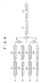
- the main CPU 44 In the step S1, the main CPU 44 generates a command for initializing the frame memory 58 provided to the GPU 49, and stores it in the main memory 45.
- the "command” means a command for setting the drawing region 58-1 and display region 58-2 in the frame memory 58 (refer to Fig. 12), and a command for setting the offset of the coordinate and so on.
- the main DMAC 46 transmits the above-mentioned commands stored in the main memory 45 to the GPU 49 through the GPUIF 72.
- the main DMAC 46 transmits the texture data which is previously stored in the main memory 45 and CLUT (Color Look Up Table) data to the GPU 49 through the GPUIF 72, and disposes them in the texture buffer 58-3 of the frame memory 58.
- CLUT Color Look Up Table
- the main CPU 44 calculates the polygon definition information comprising vertex information, shading mode information, texture information; and vertex color information required for drawing using the first vector processing engine (VPEO) 71, and stores it in the main memory 45.
- VPEO vector processing engine
- step S4 the main DMAC 46 starts transmission processing of the polygon definition information stored on the main memory 45 to the GPU 49 through the GPUIF 72.
- the GPU 49 performs texture mapping processing and starts drawing of the polygon image on the drawing region 58 of the frame memory 58 according to the polygon definition information transmitted through the GPUIF 72 as shown in Fig. 13A.
- the main CPU 44 stores the polygon definition information for drawing the image on the display region 58-2 using the polygon image data in the main memory 45.
- the main DMAC 46 transmits the polygon definition information stored in the main memory 45 in these step S6 to the GPU 49 through the GPUIF 72.
- the GPU 49 draws the reduced polygon image regarded as a texture on the display region 58-2 as shown in Fig. 13B.
- the GPU 49 performs reduction processing of the polygon image regarded as a texture using the Bi-linear texture mapping method described hereinafter.
- the PDC 84 outputs a video signal corresponding to the image drawn on the display region 58-2, and the video signal is displayed on a display device 200.
- step S9 the main CPU judges whether the above-mentioned polygon processing is completed on every frames. If the judgement indicates that polygon processing is completed not on every frames, the sequence returns to the step S2, and the processing of the step S2 and after the step S2 is performed. In the step S5, as shown in Fig. 13C, a polygon image to be displayed in the next frame is drawn on the drawing region 58-1. On the other hand, if the main CPU 44 judges polygon processing to have been completed on every frames, then the processing is brought to an end.
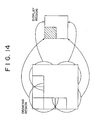
- Fig. 14 shows an arbitrary 4 ⁇ 4 pixel region on the drawing region of the frame memory 58 and a 2 ⁇ 2 pixel region corresponding to the above-mentioned 4 ⁇ 4 pixel region on the display region 58-2.
- Color resolution of each pixel drawn on the drawing region 58-1 is 16 bit direct color.
- each pixel has 16 bits comprising 5 bits respectively for R, G, and B and 1 bit for alpha bit.
- a pixel value represented by 5 bits of 2 ⁇ 2 pixels located at the upper left corner out of the 4 ⁇ 4 pixels are extracted, and these pixels are inputted to the texture read sections 101 to 104 of the average value output circuit shown in Fig. 9.
- the inputted respective pixel values are shifted by 3 bits respectively in the MSB direction in the shifters 105 to 108, thereby the value is multiplied by 8 to convert it to 8 bit value.
- These values are added by the adders 109, 110, and 111, and shifted by 2 bits in the LSB direction by the shifter 112, thereby the value is divided by 4. Thereby, an average of the value that 4 pixels are multiplied by 8 to convert it to 8 bit value is obtained.
- alpha information items having 1 bit of the respective pixels are inputted to the texture read sections 121 to 124 of the alpha value output circuit shown in Fig. 10.
- the comparators 125 to 128 detects whether the input alpha information is 0 or 1, and depending on the detection result, any one of alpha values stored in the alpha register 129 and alpha register 130 is replaced with the input respective alpha information.
- the alpha value set in the alpha registers 129 and 130 can be changed, for example, every one polygon.
- the respective alpha values of the four pixels having replaced alpha information are added by the adders 131 to 133, and then it is divided by 4 to calculate the average value of the respective alpha values of the four pixels corresponding to the respective alpha information items.
- the average value of the alpha value having 8 bits is supplied to the pixel write section 135, and written on the display region 58-2 of the frame memory 58 through the MEMIF 94. Hence, the pixels located at the upper left corner of the display region 58-2 shown in Fig. 14 is drawn.
- the PDC 84 outputs digital video signal of two series corresponding to each pixel based on the pixel value of each pixel drawn on the display region 58-2 of the frame buffer 58. One series out of two series is converted to an analog signal and then outputted as an analog video signal.
- 16 bit direct color image having 5 bits of R component, 5 bits of G component, 5 bits of B component, and 1 bit of alpha information drawn on the drawing region 58-1 is reduced to 1/2 respectively in horizontal and vertical direction (the number of pixels are reduced to 1/4), and is drawn on the display region 58-2 in the form of 24 bit full color image. Because information of 4 pixels of the image drawn on the drawing region 58-1 is reflected on each pixel of the image drawn on the display region 58-2 by the above-mentioned over-sampling, the resultant image contains substantially the information of precision finer than one pixel for one pixel. Therefore, it is possible to display an image which is clear and sharp at the polygon periphery, namely the edge, of the displayed image which is read out from the display region and displayed by the display device and has high resolution.
- drawing resolution can be enhanced to a level finer than display resolution, and the enhanced resolution allows memory use to be reduced without deterioration of drawing quality.
- enhanced resolution leads to fine graphical drawing regardless of display resolution.
- an image of high resolution finer than the display resolution can be displayed.
- color resolution per one drawing pixel can be reduced from that of display pixel, therefore memory use can be reduced.
- a pixel value average of 4 pixels is calculated in Bi-linear texture sampling.
- a pixel value average of arbitrary number of pixels may be calculated.
Landscapes
- Engineering & Computer Science (AREA)
- Physics & Mathematics (AREA)
- Computer Hardware Design (AREA)
- General Physics & Mathematics (AREA)
- Theoretical Computer Science (AREA)
- Image Generation (AREA)
Applications Claiming Priority (2)
| Application Number | Priority Date | Filing Date | Title |
|---|---|---|---|
| JP5142397 | 1997-03-06 | ||
| JP51423/97 | 1997-03-06 |
Publications (1)
| Publication Number | Publication Date |
|---|---|
| EP0863497A1 true EP0863497A1 (de) | 1998-09-09 |
Family
ID=12886526
Family Applications (1)
| Application Number | Title | Priority Date | Filing Date |
|---|---|---|---|
| EP98301603A Withdrawn EP0863497A1 (de) | 1997-03-06 | 1998-03-04 | Einrichtung zur Generierung vong raphischen Daten mit Bereichen im Pufferspeicher für normale und verkleinerte grafische Daten |
Country Status (2)
| Country | Link |
|---|---|
| US (1) | US6151035A (de) |
| EP (1) | EP0863497A1 (de) |
Families Citing this family (7)
| Publication number | Priority date | Publication date | Assignee | Title |
|---|---|---|---|---|
| RU2000102896A (ru) * | 1998-05-20 | 2001-12-20 | Сони Компьютер Энтертейнмент Инк (Jp) | Устройство и способ обработки изображений и носитель информации |
| US6556210B1 (en) * | 1998-05-29 | 2003-04-29 | Canon Kabushiki Kaisha | Image processing method and apparatus therefor |
| US6553153B1 (en) * | 1998-12-03 | 2003-04-22 | Chips And Technologies, Llc. | Method and apparatus for reducing video data |
| US20070299901A1 (en) * | 2006-06-21 | 2007-12-27 | Chunghwa Picture Tubes, Ltd. | Division unit, image analysis unit and display apparatus using the same |
| US8456478B2 (en) * | 2008-10-30 | 2013-06-04 | Microchip Technology Incorporated | Microcontroller with integrated graphical processing unit |
| US20120036301A1 (en) * | 2010-08-03 | 2012-02-09 | Caspole Eric R | Processor support for filling memory regions |
| CN103578553B (zh) * | 2013-10-14 | 2016-03-30 | 江苏敏行信息技术有限公司 | 一种矢量线型快速擦除方法 |
Citations (5)
| Publication number | Priority date | Publication date | Assignee | Title |
|---|---|---|---|---|
| WO1992003815A1 (en) * | 1990-08-28 | 1992-03-05 | Avesco Plc | Video image formation |
| EP0476409A2 (de) * | 1990-09-04 | 1992-03-25 | Kabushiki Kaisha Toshiba | Bildanzeigevorrichtung |
| EP0620532A2 (de) * | 1993-04-15 | 1994-10-19 | Sony Corporation | Verfahren und Vorrichtung zur Erzeugung eines dreidimensionalen Bildsignals und zu dessen zweidimensionalen Anzeige |
| GB2296155A (en) * | 1994-06-22 | 1996-06-19 | Microsoft Corp | Data decompression circuit |
| EP0747825A2 (de) * | 1995-06-06 | 1996-12-11 | Hewlett-Packard Company | SDRAM-Datenzuweisungsanordnung und -verfahren |
Family Cites Families (4)
| Publication number | Priority date | Publication date | Assignee | Title |
|---|---|---|---|---|
| TW278162B (de) * | 1994-10-07 | 1996-06-11 | Yamaha Corp | |
| JP3652417B2 (ja) * | 1995-10-19 | 2005-05-25 | 富士写真フイルム株式会社 | 画像処理装置 |
| US5760783A (en) * | 1995-11-06 | 1998-06-02 | Silicon Graphics, Inc. | Method and system for providing texture using a selected portion of a texture map |
| US5877771A (en) * | 1996-07-12 | 1999-03-02 | Silicon Graphics, Inc. | Method and apparatus for supersampling based on the local rate of change in texture |
-
1998
- 1998-03-04 EP EP98301603A patent/EP0863497A1/de not_active Withdrawn
- 1998-03-05 US US09/035,553 patent/US6151035A/en not_active Expired - Lifetime
Patent Citations (5)
| Publication number | Priority date | Publication date | Assignee | Title |
|---|---|---|---|---|
| WO1992003815A1 (en) * | 1990-08-28 | 1992-03-05 | Avesco Plc | Video image formation |
| EP0476409A2 (de) * | 1990-09-04 | 1992-03-25 | Kabushiki Kaisha Toshiba | Bildanzeigevorrichtung |
| EP0620532A2 (de) * | 1993-04-15 | 1994-10-19 | Sony Corporation | Verfahren und Vorrichtung zur Erzeugung eines dreidimensionalen Bildsignals und zu dessen zweidimensionalen Anzeige |
| GB2296155A (en) * | 1994-06-22 | 1996-06-19 | Microsoft Corp | Data decompression circuit |
| EP0747825A2 (de) * | 1995-06-06 | 1996-12-11 | Hewlett-Packard Company | SDRAM-Datenzuweisungsanordnung und -verfahren |
Also Published As
| Publication number | Publication date |
|---|---|
| US6151035A (en) | 2000-11-21 |
Similar Documents
| Publication | Publication Date | Title |
|---|---|---|
| KR100422082B1 (ko) | 묘화장치및묘화방법 | |
| JP4719363B2 (ja) | 内部フレームバッファと主メモリ間でのコピーアウト変換を有するグラフィクスシステム | |
| KR100574786B1 (ko) | 묘화장치, 묘화방법 및 기록매체 | |
| KR100392808B1 (ko) | 화상데이터생성방법과화상데이터처리장치및기록매체 | |
| US6362827B1 (en) | Apparatus and method for displaying a plurality of generated video images and externally supplied image data | |
| US20090278845A1 (en) | Image generating device, texture mapping device, image processing device, and texture storing method | |
| EP1312047B1 (de) | Verfahren und gerät zur unverfälschten bildwiedergabe | |
| US6441818B1 (en) | Image processing apparatus and method of same | |
| US6339430B1 (en) | Video game machine and method for changing texture of models | |
| KR100471905B1 (ko) | 메모리액세스방법및데이터처리장치 | |
| US6151035A (en) | Method and system for generating graphic data | |
| JP3548642B2 (ja) | 画像情報生成装置及び方法、画像情報処理装置及び方法、並びに記録媒体 | |
| US20020060687A1 (en) | Texture rendering method, entertainment apparatus and storage medium | |
| JP3548648B2 (ja) | 描画装置及び描画方法 | |
| US6900804B1 (en) | Method of forming polygon image and image processing apparatus using the same | |
| JP3910259B2 (ja) | 画像処理装置および方法、並びにレンダリング装置および方法 | |
| JP3971448B2 (ja) | 描画装置及び描画方法 | |
| US6624820B2 (en) | Graphic processing method for determining representative texture data for a plurality of pixels and apparatus for same | |
| JP2000348196A (ja) | 3次元画像生成装置および環境マップの生成方法 | |
| JPH10307577A (ja) | 画像データ生成装置、画像データ表示システム、および画像データ生成方法 | |
| JP3934111B2 (ja) | 描画装置及び描画方法 | |
| JP4313892B2 (ja) | 描画装置および描画方法、記録媒体 | |
| JP2583379B2 (ja) | 疑似3次元画像合成装置及び画像合成方法 | |
| MXPA97007536A (en) | Apparatus for general directions, apparatus for exhibiting images, method for generating addresses and method for exhibiting image | |
| WO1996011463A1 (fr) | Procede et dispositif de commande d'une memoire d'images completes |
Legal Events
| Date | Code | Title | Description |
|---|---|---|---|
| PUAI | Public reference made under article 153(3) epc to a published international application that has entered the european phase |
Free format text: ORIGINAL CODE: 0009012 |
|
| AK | Designated contracting states |
Kind code of ref document: A1 Designated state(s): BE DE ES FR GB IT NL SE |
|
| AX | Request for extension of the european patent |
Free format text: AL;LT;LV;MK;RO;SI |
|
| 17P | Request for examination filed |
Effective date: 19990216 |
|
| AKX | Designation fees paid |
Free format text: BE DE ES FR GB IT NL SE |
|
| RBV | Designated contracting states (corrected) |
Designated state(s): BE DE ES FR GB IT NL SE |
|
| 17Q | First examination report despatched |
Effective date: 20071017 |
|
| STAA | Information on the status of an ep patent application or granted ep patent |
Free format text: STATUS: THE APPLICATION IS DEEMED TO BE WITHDRAWN |
|
| 18D | Application deemed to be withdrawn |
Effective date: 20080228 |