EP0860873B1 - Adhesive sheet for wafer setting and process for producing electronic components - Google Patents
Adhesive sheet for wafer setting and process for producing electronic components Download PDFInfo
- Publication number
- EP0860873B1 EP0860873B1 EP98301322A EP98301322A EP0860873B1 EP 0860873 B1 EP0860873 B1 EP 0860873B1 EP 98301322 A EP98301322 A EP 98301322A EP 98301322 A EP98301322 A EP 98301322A EP 0860873 B1 EP0860873 B1 EP 0860873B1
- Authority
- EP
- European Patent Office
- Prior art keywords
- antiexpansibility
- adhesive sheet
- wafer setting
- film
- adhesive
- Prior art date
- Legal status (The legal status is an assumption and is not a legal conclusion. Google has not performed a legal analysis and makes no representation as to the accuracy of the status listed.)
- Expired - Lifetime
Links
Images
Classifications
-
- C—CHEMISTRY; METALLURGY
- C09—DYES; PAINTS; POLISHES; NATURAL RESINS; ADHESIVES; COMPOSITIONS NOT OTHERWISE PROVIDED FOR; APPLICATIONS OF MATERIALS NOT OTHERWISE PROVIDED FOR
- C09J—ADHESIVES; NON-MECHANICAL ASPECTS OF ADHESIVE PROCESSES IN GENERAL; ADHESIVE PROCESSES NOT PROVIDED FOR ELSEWHERE; USE OF MATERIALS AS ADHESIVES
- C09J7/00—Adhesives in the form of films or foils
- C09J7/20—Adhesives in the form of films or foils characterised by their carriers
- C09J7/22—Plastics; Metallised plastics
-
- H—ELECTRICITY
- H10—SEMICONDUCTOR DEVICES; ELECTRIC SOLID-STATE DEVICES NOT OTHERWISE PROVIDED FOR
- H10W—GENERIC PACKAGES, INTERCONNECTIONS, CONNECTORS OR OTHER CONSTRUCTIONAL DETAILS OF DEVICES COVERED BY CLASS H10
- H10W72/00—Interconnections or connectors in packages
- H10W72/30—Die-attach connectors
-
- H—ELECTRICITY
- H10—SEMICONDUCTOR DEVICES; ELECTRIC SOLID-STATE DEVICES NOT OTHERWISE PROVIDED FOR
- H10W—GENERIC PACKAGES, INTERCONNECTIONS, CONNECTORS OR OTHER CONSTRUCTIONAL DETAILS OF DEVICES COVERED BY CLASS H10
- H10W72/00—Interconnections or connectors in packages
- H10W72/071—Connecting or disconnecting
- H10W72/073—Connecting or disconnecting of die-attach connectors
-
- H—ELECTRICITY
- H10—SEMICONDUCTOR DEVICES; ELECTRIC SOLID-STATE DEVICES NOT OTHERWISE PROVIDED FOR
- H10W—GENERIC PACKAGES, INTERCONNECTIONS, CONNECTORS OR OTHER CONSTRUCTIONAL DETAILS OF DEVICES COVERED BY CLASS H10
- H10W72/00—Interconnections or connectors in packages
- H10W72/071—Connecting or disconnecting
- H10W72/073—Connecting or disconnecting of die-attach connectors
- H10W72/07331—Connecting techniques
- H10W72/07337—Connecting techniques using a polymer adhesive, e.g. an adhesive based on silicone or epoxy
-
- H—ELECTRICITY
- H10—SEMICONDUCTOR DEVICES; ELECTRIC SOLID-STATE DEVICES NOT OTHERWISE PROVIDED FOR
- H10W—GENERIC PACKAGES, INTERCONNECTIONS, CONNECTORS OR OTHER CONSTRUCTIONAL DETAILS OF DEVICES COVERED BY CLASS H10
- H10W72/00—Interconnections or connectors in packages
- H10W72/30—Die-attach connectors
- H10W72/351—Materials of die-attach connectors
- H10W72/353—Materials of die-attach connectors not comprising solid metals or solid metalloids, e.g. ceramics
- H10W72/354—Materials of die-attach connectors not comprising solid metals or solid metalloids, e.g. ceramics comprising polymers
-
- Y—GENERAL TAGGING OF NEW TECHNOLOGICAL DEVELOPMENTS; GENERAL TAGGING OF CROSS-SECTIONAL TECHNOLOGIES SPANNING OVER SEVERAL SECTIONS OF THE IPC; TECHNICAL SUBJECTS COVERED BY FORMER USPC CROSS-REFERENCE ART COLLECTIONS [XRACs] AND DIGESTS
- Y10—TECHNICAL SUBJECTS COVERED BY FORMER USPC
- Y10S—TECHNICAL SUBJECTS COVERED BY FORMER USPC CROSS-REFERENCE ART COLLECTIONS [XRACs] AND DIGESTS
- Y10S156/00—Adhesive bonding and miscellaneous chemical manufacture
- Y10S156/918—Delaminating processes adapted for specified product, e.g. delaminating medical specimen slide
- Y10S156/93—Semiconductive product delaminating, e.g. delaminating emiconductive wafer from underlayer
-
- Y—GENERAL TAGGING OF NEW TECHNOLOGICAL DEVELOPMENTS; GENERAL TAGGING OF CROSS-SECTIONAL TECHNOLOGIES SPANNING OVER SEVERAL SECTIONS OF THE IPC; TECHNICAL SUBJECTS COVERED BY FORMER USPC CROSS-REFERENCE ART COLLECTIONS [XRACs] AND DIGESTS
- Y10—TECHNICAL SUBJECTS COVERED BY FORMER USPC
- Y10S—TECHNICAL SUBJECTS COVERED BY FORMER USPC CROSS-REFERENCE ART COLLECTIONS [XRACs] AND DIGESTS
- Y10S438/00—Semiconductor device manufacturing: process
- Y10S438/976—Temporary protective layer
-
- Y—GENERAL TAGGING OF NEW TECHNOLOGICAL DEVELOPMENTS; GENERAL TAGGING OF CROSS-SECTIONAL TECHNOLOGIES SPANNING OVER SEVERAL SECTIONS OF THE IPC; TECHNICAL SUBJECTS COVERED BY FORMER USPC CROSS-REFERENCE ART COLLECTIONS [XRACs] AND DIGESTS
- Y10—TECHNICAL SUBJECTS COVERED BY FORMER USPC
- Y10T—TECHNICAL SUBJECTS COVERED BY FORMER US CLASSIFICATION
- Y10T156/00—Adhesive bonding and miscellaneous chemical manufacture
- Y10T156/11—Methods of delaminating, per se; i.e., separating at bonding face
-
- Y—GENERAL TAGGING OF NEW TECHNOLOGICAL DEVELOPMENTS; GENERAL TAGGING OF CROSS-SECTIONAL TECHNOLOGIES SPANNING OVER SEVERAL SECTIONS OF THE IPC; TECHNICAL SUBJECTS COVERED BY FORMER USPC CROSS-REFERENCE ART COLLECTIONS [XRACs] AND DIGESTS
- Y10—TECHNICAL SUBJECTS COVERED BY FORMER USPC
- Y10T—TECHNICAL SUBJECTS COVERED BY FORMER US CLASSIFICATION
- Y10T428/00—Stock material or miscellaneous articles
- Y10T428/21—Circular sheet or circular blank
- Y10T428/218—Aperture containing
-
- Y—GENERAL TAGGING OF NEW TECHNOLOGICAL DEVELOPMENTS; GENERAL TAGGING OF CROSS-SECTIONAL TECHNOLOGIES SPANNING OVER SEVERAL SECTIONS OF THE IPC; TECHNICAL SUBJECTS COVERED BY FORMER USPC CROSS-REFERENCE ART COLLECTIONS [XRACs] AND DIGESTS
- Y10—TECHNICAL SUBJECTS COVERED BY FORMER USPC
- Y10T—TECHNICAL SUBJECTS COVERED BY FORMER US CLASSIFICATION
- Y10T428/00—Stock material or miscellaneous articles
- Y10T428/24—Structurally defined web or sheet [e.g., overall dimension, etc.]
- Y10T428/24479—Structurally defined web or sheet [e.g., overall dimension, etc.] including variation in thickness
- Y10T428/24488—Differential nonuniformity at margin
-
- Y—GENERAL TAGGING OF NEW TECHNOLOGICAL DEVELOPMENTS; GENERAL TAGGING OF CROSS-SECTIONAL TECHNOLOGIES SPANNING OVER SEVERAL SECTIONS OF THE IPC; TECHNICAL SUBJECTS COVERED BY FORMER USPC CROSS-REFERENCE ART COLLECTIONS [XRACs] AND DIGESTS
- Y10—TECHNICAL SUBJECTS COVERED BY FORMER USPC
- Y10T—TECHNICAL SUBJECTS COVERED BY FORMER US CLASSIFICATION
- Y10T428/00—Stock material or miscellaneous articles
- Y10T428/24—Structurally defined web or sheet [e.g., overall dimension, etc.]
- Y10T428/24942—Structurally defined web or sheet [e.g., overall dimension, etc.] including components having same physical characteristic in differing degree
-
- Y—GENERAL TAGGING OF NEW TECHNOLOGICAL DEVELOPMENTS; GENERAL TAGGING OF CROSS-SECTIONAL TECHNOLOGIES SPANNING OVER SEVERAL SECTIONS OF THE IPC; TECHNICAL SUBJECTS COVERED BY FORMER USPC CROSS-REFERENCE ART COLLECTIONS [XRACs] AND DIGESTS
- Y10—TECHNICAL SUBJECTS COVERED BY FORMER USPC
- Y10T—TECHNICAL SUBJECTS COVERED BY FORMER US CLASSIFICATION
- Y10T428/00—Stock material or miscellaneous articles
- Y10T428/24—Structurally defined web or sheet [e.g., overall dimension, etc.]
- Y10T428/24942—Structurally defined web or sheet [e.g., overall dimension, etc.] including components having same physical characteristic in differing degree
- Y10T428/2495—Thickness [relative or absolute]
-
- Y—GENERAL TAGGING OF NEW TECHNOLOGICAL DEVELOPMENTS; GENERAL TAGGING OF CROSS-SECTIONAL TECHNOLOGIES SPANNING OVER SEVERAL SECTIONS OF THE IPC; TECHNICAL SUBJECTS COVERED BY FORMER USPC CROSS-REFERENCE ART COLLECTIONS [XRACs] AND DIGESTS
- Y10—TECHNICAL SUBJECTS COVERED BY FORMER USPC
- Y10T—TECHNICAL SUBJECTS COVERED BY FORMER US CLASSIFICATION
- Y10T428/00—Stock material or miscellaneous articles
- Y10T428/28—Web or sheet containing structurally defined element or component and having an adhesive outermost layer
- Y10T428/2848—Three or more layers
Definitions
- the present invention has been made with a view toward resolving the above problem of the prior art.
- the process for producing an electronic component according to the present invention comprises a step of expanding an adhesive sheet, wherein the above adhesive sheet for wafer setting according to the present invention is used as the adhesive sheet.
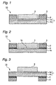
- the antiexpansibility increasing film 2 may be disposed on the marginal part of the adhesive layer 1a of the adhesive sheet 1, as shown in Fig. 1.
- the antiexpansibility increasing film 2 may be laminated either directly or through the medium of an adhesive layer 4 onto the marginal part of the surface of the expansible film 1b.
- the antiexpansibility increasing film 2 may be laminated either directly or through the medium of an adhesive layer 4 onto another surface (back of the expansible film 1b) of the expansible film 1b opposite to the adhesive layer.
- the expansible film 1b is not particularly limited, it is preferred that the expansible film have high water and heat resistances and be composed of a synthetic resin.
- suitable expansible films 1b include films of low density polyethylene (LDPE), linear low density polyethylene (LLDPE), ethylene/propylene copolymer, polypropylene, polybutene, polybutadiene, polymethylpentene, ethylene/vinyl acetate copolymer, ethylene/ (meth(meth)acrylic acid copolymer, ethylene/methyl(meth)acrylate copolymer, ethylene/ethyl (meth)acrylate copolymer, polyvinyl chloride, vinyl chloride/vinyl acetate copolymer, ethylene/vinyl chloride/vinyl acetate copolymer, polyurethanes, polyamides, ionomers, styrene/butadiene rubber and products of hydrogenation or other modification of styrene/butadiene rubber.
- LDPE low density polyethylene
- LLDPE linear low density polyethylene
- ethylene/propylene copolymer polypropylene
- the antiexpansibility increasing film 2 and the expansible film 1b can be laminated onto each other by, for example, heat sealing.
Landscapes
- Chemical & Material Sciences (AREA)
- Organic Chemistry (AREA)
- Dicing (AREA)
- Adhesive Tapes (AREA)
- Adhesives Or Adhesive Processes (AREA)
- Laminated Bodies (AREA)
Description
- The present invention relates to an adhesive sheet for wafer setting and a process for producing an electronic component. More particularly, the present invention is concerned with an adhesive sheet for wafer setting and a process for producing an electronic component, by which an expanding step can securely be performed in the production of small electronic components such as semiconductor chips.
- A semiconductor wafer of, for example, silicon or gallium arsenide is produced in a large diameter, cut and separated (diced) into elemental chips and subjected to the subsequent mounting step. In this process, the semiconductor wafer undergoes dicing and expansion steps whilst being attached to an adhesive sheet and is transferred to the subsequent pickup and mounting steps.
- In the expansion step, the adhesive sheet is extended so that chip spacings are expanded. The objective of the expansion step in which chip spacings are expanded is, for example, to facilitate chip recognition in the die bonding and to prevent device breakage attributed to mutual abuttal of neighboring chips in the pickup step.
- Currently, the expansion step is carried out by extending the adhesive sheet with the use of an expanding apparatus.
- JP-A-02 265 258 discloses a dicing apparatus for integrated circuit chips. A carrier supports a peripheral edge of a stretching filmlike base material. A partial range on the surface of the base material is coated with an adhesive material whose adhesive strength is lowered under ultraviolet irradiation.
- In most expanding apparatus, the degree of extension and the torque during the extension are fixed to thereby render difficult adjustment dependent upon the type of adhesive sheet and the size of device.
- Accordingly, it has been the case that, when the adhesive sheet is soft, the extending stress is not conveyed to the wafer setting portion, thereby not resulting in the attainment of satisfactory chip spacings and that, on the other hand when the adhesive sheet is hard, the torque of the apparatus is unsatisfactory or the adhesive sheet is torn.
- The present invention has been made with a view toward resolving the above problem of the prior art.
- The object of the present invention is to enable the secure performance of an expansion in the production of electronic components.
- The present invention relates to an adhesive sheet for wafer setting comprising:
- a wafer setting part comprising an expansible film and an adhesive layer for wafer setting; and
- a marginal part outside of said wafer setting part and at least inside of the part of the adhesive sheet to which a ring frame can be applied, characterised in that:
- said marginal part has an antiexpansibility
expressed by the following formula:
-
- In the present invention, it is preferred that the antiexpansibility of the marginal part be at least 1.3 times that of the wafer setting part.
- For example, the above adhesive sheet for wafer setting comprises an adhesive sheet comprising an expansible film and an adhesive layer for wafer setting, this adhesive sheet having a marginal part to which an antiexpansibility increasing film is laminated.
- The process for producing an electronic component according to the present invention comprises a step of expanding an adhesive sheet,
wherein the above adhesive sheet for wafer setting according to the present invention is used as the adhesive sheet. - In the accompanying drawings:
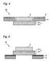
- Figures 1 to 5 show varieties of adhesive sheet for wafer setting according to the present invention;
-
- The present invention will be described in detail below, referring to the appended drawings.
- In particular, referring to Figs. 1 to 5, the adhesive sheet for wafer setting 10 according to the present invention has a fundamental structure consisting of any of various conventional generally employed
adhesive sheets 1 comprising a wafer setting part composed of anexpansible film 1b and an adhesive layer forwafer setting 1a. The adhesive sheet for wafer setting 10 according to the present invention is characterized in that the antiexpansibility of a marginal part of theadhesive sheet 1 is greater than that of the wafer setting parts. - In the above adhesive sheet for wafer setting 10, the terminology "marginal part" refers to the parts of the sheet which lie at least inside of the ring frame fixed part and which exclude the part on which wafers 3 (indicated by broken lines in the drawings) are set.
- The terminology "antiexpansibility" means the magnitude of stress transmittability from one site to a neighboring site. In the present invention, the antiexpansibility is evaluated by the value defined by the formula:
- For example, in the adhesive sheet for wafer setting 10 structured as shown in Fig. 1, the antiexpansibility of the wafer setting part is given by (elastic modulus of adhesive layer for
wafer setting 1a) x (thickness of adhesive layer forwafer setting 1a) + (elastic modulus ofexpansible film 1b) x (thickness ofexpansible film 1b). - On the other hand, the antiexpansibility of the marginal part is given by (elastic modulus of adhesive layer for
wafer setting 1a) x (thickness of adhesive layer forwafer setting 1a) + (elastic modulus ofexpansible film 1b) x (thickness ofexpansible film 1b) + (elastic modulus of antiexpansibility increasing film 2) x (thickness of antiexpansibility increasing film 2) + (elastic modulus of adhesive layer 5) x (thickness of adhesive layer 5). - In the present invention, the antiexpansibility of the above marginal part is greater than that of the wafer setting part. It is preferred that the antiexpansibility of the marginal part be at least 1.3 times, especially, at least 1.5 time that of the wafer setting part.
- The above adhesive sheet for
wafer setting 10, for example, comprises a generally employedadhesive sheet 1 comprising anexpansible film 1b and an adhesive layer forwafer setting 1a, thisadhesive sheet 1 having a marginal part to which anantiexpansibility increasing film 2 is laminated. - The
antiexpansibility increasing film 2 may be disposed on the marginal part of theadhesive layer 1a of theadhesive sheet 1, as shown in Fig. 1. Referring to Fig. 2, when theadhesive layer 1a is formed only on and around the wafer setting part of a surface of theexpansible film 1b, theantiexpansibility increasing film 2 may be laminated either directly or through the medium of anadhesive layer 4 onto the marginal part of the surface of theexpansible film 1b. Further, referring to Fig. 3, theantiexpansibility increasing film 2 may be laminated either directly or through the medium of anadhesive layer 4 onto another surface (back of theexpansible film 1b) of theexpansible film 1b opposite to the adhesive layer. Also, theantiexpansibility increasing film 2 may be disposed on both the marginal parts of the surface of theadhesive layer 1a orexpansible film 1b and the marginal part of the back of theexpansible film 1b. Still further, referring to Figs. 4 and 5, the adhesive sheet for wafer setting 10 according to the present invention may have such a structure that a marginal part forming film whose antiexpansibility is greater than that of the adhesive sheet continues from an edge of the adhesive sheet whose surface area is slightly greater than that of the wafer setting parts. - Although the
expansible film 1b is not particularly limited, it is preferred that the expansible film have high water and heat resistances and be composed of a synthetic resin. - Examples of suitable
expansible films 1b include films of low density polyethylene (LDPE), linear low density polyethylene (LLDPE), ethylene/propylene copolymer, polypropylene, polybutene, polybutadiene, polymethylpentene, ethylene/vinyl acetate copolymer, ethylene/ (meth(meth)acrylic acid copolymer, ethylene/methyl(meth)acrylate copolymer, ethylene/ethyl (meth)acrylate copolymer, polyvinyl chloride, vinyl chloride/vinyl acetate copolymer, ethylene/vinyl chloride/vinyl acetate copolymer, polyurethanes, polyamides, ionomers, styrene/butadiene rubber and products of hydrogenation or other modification of styrene/butadiene rubber. Theseexpansible films 1b can be used in combination. Moreover, use can be made of a film of a polymer of a compound having a carboxyl group as a polymer structural unit and a laminate of this film and a generally employed polymer film. - The thickness of the above
expansible film 1b generally ranges from 5 to 500 µm, preferably, from 10 to 300 µm. It is preferred that the elastic modulus of theexpansible film 1b be less than 1 x 10⁹ N/m2, especially, from 1 x 10⁷ to 1 x 10⁹ N/m2. Thus, it is preferred that the antiexpansibility of theexpansible film 1b be less than 5 x 10⁵ N/m, especially, from 1 x 10² to 3 x 10⁵ N/m. - The side of the
expansible film 1b brought into contact with another layer may be provided with corona treatment or may have a primer or other layer attached thereto for improving the adherence. - In the present invention, the adhesive layer for wafer setting may be irradiated with ultraviolet rays prior to or after the dicing step. When the irradiation is effected, the
expansible film 1b must be transparent. - The adhesive layer for
wafer setting 1a can be produced from various conventional adhesives. These adhesives are not particularly limited and some examples thereof include adhesives based on a rubber, an acrylic, a silicone and a polyvinyl ether. Also, use can be made of adhesives which are curable by radiation and adhesives which foam when heated. Further, use can be made of adhesives usable in both dicing and die bonding. - Although depending on the properties of the materials thereof, the thickness of the
adhesive layer 1a generally ranges from about 3 to 100 µm, preferably, from about 10 to 50 µm. It is preferred that the elastic modulus of theadhesive layer 1a range from 1 x 10³ to 1 x 10⁹ N/m2, especially, from 1 x 10⁴ to 1 x 10⁸ N/m2. Thus, it is preferred that the antiexpansibility of theadhesive layer 1a range from 3 x 10⁻³ to 1 x 10⁵ N/m, especially, from 1 x 10⁻¹ to 5 x 10³ N/m. - The adhesive layer for
wafer setting 1a may be cured by heating or irradiation with ultraviolet rays prior to the expanding step to thereby have a change of elastic modulus. The elastic modulus at the expanding step contributes to the antiexpansibility thereof. - Polyethylene terephthalate and polybutylene terephthalate in addition to polymers set forth above as materials of the expansible film can be mentioned as materials of the
antiexpansibility increasing film 2. - Although depending on the properties of the materials thereof, the thickness of the
antiexpansibility increasing film 2 generally ranges from about 5 to 500 µm, preferably, from about 10 to 300 µm. It is preferred that the elastic modulus of theantiexpansibility increasing film 2 range from 1 x 10⁷ to 1 x 10¹⁰ N/m2, especially, from 5 x 10⁷ to 5 x 10⁹ N/m2. Thus, it is preferred that the antiexpansibility of theantiexpansibility increasing film 2 range from 5 x 101 to 5 x 10⁶ N/m, especially, from 5 x 10² to 1.5 x 10⁶ N/m. - In the structure of Fig. 1 or Fig. 4, the
antiexpansibility increasing film 2 is laminated onto theadhesive layer 1a of theadhesive sheet 1. - In the structure of Fig. 2, Fig. 3 or Fig. 5, the antiexpansibility increasing film is laminated directly or through the medium of an
adhesive layer 4 onto theexpansible film 1b. - The adhesive employed for bonding the
antiexpansibility increasing film 2 with theexpansible film 1b is not particularly limited and generally used adhesives may be employed. Examples of suitable adhesives include adhesives such as those based on an acrylic, a rubber and a silicone and thermoplastic or thermosetting adhesives such as those based on a polyester, a polyamide, an ethylene copolymer, an epoxy and a urethane. - Although depending on the properties of the materials thereof, the thickness of the
adhesive layer 4 generally ranges from about 3 to 50 µm, preferably, from about 5 to 30 µm. It is preferred that the elastic modulus of theadhesive layer 4 range from 1 x 10³ to 1 x 10⁹ N/m2, especially, from 1 x 10⁴ to 1 x 10⁸ N/m2. Thus, it is preferred that the antiexpansibility of theadhesive layer 4 range from 3 x 10⁻³ to 5 x 10⁴ N/m, especially, from 5 x 10⁻² to 3 x 10³ N/m. - Also, without the use of the
adhesive layer 4, theantiexpansibility increasing film 2 and theexpansible film 1b can be laminated onto each other by, for example, heat sealing. - In the structure of Fig. 1 or Fig. 2, it is preferred that an
adhesive layer 5 be disposed on theantiexpansibility increasing film 2. Theadhesive layer 5 is used for fixing a ring frame. The ring frame is a jig for conveyance and processing which supports the wafer during the dicing step and the bonding step, etc. - Although depending on the properties of the materials thereof, the thickness of the
adhesive layer 5 generally ranges from about 3 to 50 µm, preferably, from about 5 to 30 µm. It is preferred that the elastic modulus of theadhesive layer 5 range from 1 x 10³ to 1 x 10⁹ N/m2, especially, from 1 x 10⁴ to 1 x 10⁸ N/m2. Thus, it is preferred that the antiexpansibility of theadhesive layer 5 range from 3 x 10⁻³ to 5 x 10⁴ N/m, especially, from 5 x 10⁻² to 3 x 10³ N/m. - It is not necessarily required that the
antiexpansibility increasing film 2 be formed in a circularly continued shape. Theantiexpansibility increasing film 2 may be formed discontinuously on the marginal part of the adhesive sheet for wafer setting 10. - The process for producing an electronic component according to the present invention will now be described.
- The process for producing an electronic component according to the present invention comprises a step of expanding an adhesive sheet,
wherein the above adhesive sheet for wafer setting according to the present invention is used as the adhesive sheet. - More particularly, in the common process for producing an electronic component, namely, in the process including the steps of sticking a wafer to an adhesive sheet, dicing the wafer into chips, expanding the adhesive sheet having the chips stuck thereto to thereby extend chip spacings, picking the chips up and assembling the chips into electronic components, the improvement comprises reinforcing a marginal part of the adhesive sheet for wafer setting with an antiexpansibility increasing film prior to the expanding step. Those described above are used as the adhesive sheet and the antiexpansibility increasing film.
- In the process of the present invention, the above adhesive sheet for wafer setting 10 having the
antiexpansibility increasing film 2 or thecommon adhesive sheet 1 whose marginal part is not reinforced can be used as the adhesive sheet for wafer setting 10. - When the adhesive sheet for wafer setting 10 having the
antiexpansibility increasing film 2 is employed, it is naturally unnecessary to stick a newantiexpansibility increasing film 2 thereto. The reason is that, prior to the expanding step, the marginal part of the adhesive sheet for wafer setting is reinforced by the antiexpansibility increasing film. - On the other hand, when the
common adhesive sheet 1 whose marginal part is not reinforced is employed, an antiexpansibility increasing film is stuck to appropriate positions at any of the steps prior to the expanding step. That is, the antiexpansibility increasing film is stuck to the marginal part of the adhesive sheet at any of stages preceding or ensuing the sticking of the wafer to the adhesive sheet, preceding or ensuing the dicing of the wafer into chips and preceding the expansion of the adhesive sheet. - Asis apparent from the foregoing, the present invention causes the antiexpansibility of the marginal part of the adhesive sheet for wafer setting 10 to be greater than that of the wafer setting part of the adhesive sheet for wafer setting 10, thereby preventing extension of only the marginal part of the sheet at the time of the expansion. As a result, the stress is transmitted without being damped to the part having the wafer stuck thereto (namely, a part having a multiplicity of chips fixed thereto), so that the chip spacings are satisfactorily extended to thereby enable minimization of malfunctions at the time of picking up of the chips.
- The present invention will be illustrated in detail below with reference to the following Examples.
- In the following Examples and Comparative Example, the chip spacing was evaluated in the following manner.
- A 15.24 cm (6 inch) silicon wafer was set on the adhesive layer of the adhesive sheet for wafer setting produced in each of the following Examples and Comparative Examples, and the adhesive sheet for wafer setting was fixed by means of a ring frame. The wafer was diced by the customary procedure into 10 mm x 10 mm IC chips. Thereafter, a 15 mm expansion was carried out by the use of expander HS-1010 manufactured by HUGRE ELECTRONICS, and the chip spacings were measured by the use of an optical microscope. In Examples 1, 2, 3 and 5 and Comparative Examples 1, 2 and 3, ultraviolet irradiation (quantity of light: 220 mJ/cm2) was performed after the dicing and, thereafter, the chip spacings were measured.
- Use was made of a dicing/die bonding sheet, as an adhesive sheet, composed of an expansible film of an ethylene/methyl methacrylate copolymer (elastic modulus: 1.00 x 10⁸ N/m2, thickness: 80 µm and antiexpansibility: 8.0 x 10³ N/m) and a thermosetting adhesive layer based on acrylic polymer containing epoxy resin (elastic modulus: 3.0 x 10⁶ N/m2, thickness: 20 µm and antiexpansibility: 6.0 x 101 N/m). Prior to use, a release film (polyethylene terephthalate film, thickness: 38 µm) was stuck to the adhesive layer in order to protect the adhesive layer.
- A soft polyvinyl chloride film (elastic modulus: 1.80 x 10⁸ N/m2, thickness: 70 µm and antiexpansibility: 1.26 x 10⁴ N/m) was used as an antiexpansibility increasing film, and a repeeling type adhesive (acrylic polymer crosslinking type, elastic modulus: 3.0 x 10⁵ N/m2, thickness: 10 µm and antiexpansibility: 3.0 N/m) was used as a ring frame fixing adhesive. The employed antiexpansibility increasing film had an inside diameter of 165 mm and an outside diameter of 207 mm, which was the same as the diameter of the expansible film.
- The chip spacings of the thus obtained adhesive sheet for wafer setting were measured. The results are given in Table 1.
- The same procedure as in Example 1 was repeated except that the expansible film of Example 1 was replaced by a laminate film (30 µm/35 µm/30 µm, elastic modulus: 9.0 x 10⁷ N/m2 and antiexpansibility: 8.6 x 10³ N/m) of an ethylene/methyl methacrylate copolymer, an elastomer (modified styrene/butadiene rubber) and an ethylene/methacrylic acid copolymer. The results are given in Table 1.
- The same procedure as in Example 1 was repeated except that the expansible film of Example 1 was replaced by a laminate film (30 µm /40 µm/30 µm, elastic modulus: 5.6 x 10⁷ N/m2 and antiexpansibility: 5.6 x 10³ N/m) of an ethylene/methyl methacrylate copolymer, an elastomer (product of hydrogenation of styrene/butadiene rubber) and an ethyl one/methacrylic acid copolymer. The results are given in Table 1.
- Use was made of a dicing sheet, as an adhesive sheet, composed of an expansible film of a soft polyvinyl chloride (elastic modulus: 1.80 x 10⁸ N/m2, thickness: 100 µm and antiexpansibility: 18.0 x 10³ N/m) and an adhesive layer based on a peelable type adhesive (acrylic polymer crosslinking type, elastic modulus: 3.0 x 10⁵ N/m2, thickness: 10 µm and antiexpansibility: 3.0 N/m). Prior to use, a release film (polyethylene terephthalate film, thickness: 38 µm) was stuck to the adhesive layer in order to protect the adhesive layer.
- A soft polyvinyl chloride film (elastic modulus: 1.80 x 10⁸ N/m2, thickness: 70 µm and antiexpansibility: 12.6 x 10³ N/m) was used as an antiexpansibility increasing film, and a peelable type adhesive (acrylic polymer crosslinking type, elastic modulus: 3.0 x 10⁵ N/m2, thickness: 10 µm and antiexpansibility: 3.0 N/m) was used as a ring frame fixing adhesive. The employed antiexpansibility increasing film had an inside diameter of 165 mm and an outside diameter of 207 mm, which was the same as the diameter of the expansible film.
- The chip spacings of the thus obtained adhesive sheet for wafer setting were measured. The results are given in Table 1.
- The same procedure as in Example 2 was repeated except that a film of an ethylene/methyl methacrylate copolymer (elastic modulus: 1.35 x 10⁸ N/m2, thickness: 80 µm and antiexpansibility: 10.8 x 10³ N/m) was used as an antiexpansibility increasing film and a peelable type adhesive (acrylic polymer crosslinking type, elastic modulus: 3.0 x 10⁵ N/m2, thickness: 10 µm and antiexpansibility: 3.0 N/m) was used as a ring frame fixing adhesive. The results are given in Table 1.
- The same procedure as in Example 4 was repeated except that a film of an ethylene/methyl methacrylate copolymer (elastic modulus: 1.35 x 10⁸ N/m2, thickness: 80 µm and antiexpansibility: 10.8 x 10³ N/m) was used as an antiexpansibility increasing film and a peelable type adhesive (acrylic polymer crosslinking type, elastic modulus: 3.0 x 10⁵ N/m2, thickness: 10 µm and antiexpansibility: 3.0 N/m) was used as a ring frame fixing adhesive. The results are given in Table 1.
- The same procedure as in Example 1 was repeated except' that no antiexpansibility increasing film was used. The results are given in Table 1.
- The same procedure as in Example 2 was repeated except that no antiexpansibility increasing film was used. The results are given in Table 1.
- The same procedure as in Example 3 was repeated except that no antiexpansibility increasing film was used. The results are given in Table 1.
- The same procedure as in Example 4 was repeated except that no antiexpansibility increasing film was used. The results are given in Table 1.
Antiexpansibility (N/m) Chip spacing (µm) Wafer setting part Marginal part of sheet X-axis Y-axis Ex. 1 8.1 x 10³ 20.7 x 10³ 260 200 Ex. 2 8.7 x 10³ 21.3 x 10³ 240 230 Ex. 3 5.7 x 10³ 18.3 x 10³ 490 330 Ex. 4 18.0 x 10³ 30.6 x 10³ 290 280 Ex. 5 8.7 x 10³ 19.5 x 10³ 350 250 Ex. 6 18.0 x 10³ 28.8 x 10³ 330 270 Com. Ex.1 8.1 x 10³ 8.1 x 10³ 40 50 Com. Ex.2 8.7 x 10³ 8.7 x 10³ 70 60 Com. Ex.3 5.7 x 10³ 5.7 x 10³ 60 60 Com. Ex.4 18.0 x 10³ 18.0 x 10³ 140 130
Claims (4)
- An adhesive sheet for wafer setting comprising:characterised in that:a wafer setting part comprising an expansible film and an adhesive layer for wafer setting; anda marginal part outside of said wafer setting part and at least inside of the part of the adhesive sheet to which a ring frame can be applied,which is greater than that of the wafer setting part.said marginal part has an antiexpansibility expressed by the following formula:
- An adhesive sheet for wafer setting as claimed in claim 1, wherein the marginal part has an antiexpansibility which is at least 1.3 times that of the wafer setting part.
- An adhesive sheet for wafer setting as claimed in claim 1 wherein an antiexpansibility increasing film is laminated to said marginal part of said adhesive sheet.
- A process for producing an electronic component, comprising a step of expanding an adhesive sheet, wherein the adhesive sheet is the adhesive sheet for wafer setting as claimed in any one of claims 1 to 3.
Applications Claiming Priority (3)
| Application Number | Priority Date | Filing Date | Title |
|---|---|---|---|
| JP3919697 | 1997-02-24 | ||
| JP39196/97 | 1997-02-24 | ||
| JP9039196A JPH10242084A (en) | 1997-02-24 | 1997-02-24 | Method for producing pressure-sensitive adhesive sheet for attaching wafer and electronic component |
Publications (2)
| Publication Number | Publication Date |
|---|---|
| EP0860873A1 EP0860873A1 (en) | 1998-08-26 |
| EP0860873B1 true EP0860873B1 (en) | 2003-06-18 |
Family
ID=12546378
Family Applications (1)
| Application Number | Title | Priority Date | Filing Date |
|---|---|---|---|
| EP98301322A Expired - Lifetime EP0860873B1 (en) | 1997-02-24 | 1998-02-24 | Adhesive sheet for wafer setting and process for producing electronic components |
Country Status (7)
| Country | Link |
|---|---|
| US (1) | US6042922A (en) |
| EP (1) | EP0860873B1 (en) |
| JP (1) | JPH10242084A (en) |
| KR (1) | KR100473994B1 (en) |
| DE (1) | DE69815564T2 (en) |
| MY (1) | MY120140A (en) |
| TW (1) | TW375814B (en) |
Families Citing this family (32)
| Publication number | Priority date | Publication date | Assignee | Title |
|---|---|---|---|---|
| JP4540150B2 (en) * | 1998-09-30 | 2010-09-08 | 日東電工株式会社 | Thermally peelable adhesive sheet |
| JP2000114204A (en) * | 1998-10-01 | 2000-04-21 | Mitsubishi Electric Corp | Wafer sheet, method of manufacturing semiconductor device using the same, and semiconductor manufacturing apparatus |
| US6280822B1 (en) * | 1999-01-11 | 2001-08-28 | 3M Innovative Properties Company | Cube corner cavity based retroeflectors with transparent fill material |
| KR100689166B1 (en) * | 1999-07-06 | 2007-03-08 | 부라더 고교 가부시키가이샤 | Stamp member for stamp and stamp unit using same |
| JP4230080B2 (en) * | 2000-02-18 | 2009-02-25 | リンテック株式会社 | Wafer sticking adhesive sheet |
| US6319754B1 (en) * | 2000-07-10 | 2001-11-20 | Advanced Semiconductor Engineering, Inc. | Wafer-dicing process |
| US6531238B1 (en) | 2000-09-26 | 2003-03-11 | Reliant Energy Power Systems, Inc. | Mass transport for ternary reaction optimization in a proton exchange membrane fuel cell assembly and stack assembly |
| TWI232560B (en) * | 2002-04-23 | 2005-05-11 | Sanyo Electric Co | Semiconductor device and its manufacture |
| JP3838637B2 (en) * | 2002-06-10 | 2006-10-25 | 日東電工株式会社 | Glass substrate dicing adhesive sheet and glass substrate dicing method |
| TWI229435B (en) | 2002-06-18 | 2005-03-11 | Sanyo Electric Co | Manufacture of semiconductor device |
| US7399683B2 (en) | 2002-06-18 | 2008-07-15 | Sanyo Electric Co., Ltd. | Manufacturing method of semiconductor device |
| TWI227550B (en) * | 2002-10-30 | 2005-02-01 | Sanyo Electric Co | Semiconductor device manufacturing method |
| JP4401181B2 (en) | 2003-08-06 | 2010-01-20 | 三洋電機株式会社 | Semiconductor device and manufacturing method thereof |
| WO2005057644A1 (en) * | 2003-12-15 | 2005-06-23 | The Furukawa Electric Co., Ltd. | Wafer processing tape and method of producing the same |
| JP2005272724A (en) * | 2004-03-25 | 2005-10-06 | Furukawa Electric Co Ltd:The | Adhesive tape for semiconductor |
| DE102004021775A1 (en) * | 2004-04-30 | 2005-11-24 | Tesa Ag | Adhesive tape for masking window flanges when painting car bodywork, has a 2-layer carrier comprising a layer of plasticised polyvinyl chloride and a layer of unstretched polybutylene terephthalate, with adhesive on either layer |
| KR100865412B1 (en) * | 2004-05-18 | 2008-10-24 | 히다치 가세고교 가부시끼가이샤 | Adhesive bonding sheet, semiconductor device using same, and method for manufacturing such semiconductor device |
| US20060068576A1 (en) * | 2004-09-30 | 2006-03-30 | Burdick William E Jr | Lithography transfer for high density interconnect circuits |
| TWI324800B (en) * | 2005-12-28 | 2010-05-11 | Sanyo Electric Co | Method for manufacturing semiconductor device |
| JP2007250598A (en) * | 2006-03-14 | 2007-09-27 | Renesas Technology Corp | Manufacturing method of semiconductor device |
| KR100874953B1 (en) * | 2006-09-20 | 2008-12-19 | 삼성전자주식회사 | Semiconductor wafer holding device |
| JP2009054953A (en) * | 2007-08-29 | 2009-03-12 | Disco Abrasive Syst Ltd | Wafer processing method |
| JP2010232611A (en) * | 2009-03-30 | 2010-10-14 | Furukawa Electric Co Ltd:The | Wafer processing tape |
| JP5442308B2 (en) * | 2009-04-22 | 2014-03-12 | ルネサスエレクトロニクス株式会社 | Manufacturing method of semiconductor device |
| JP2012079936A (en) | 2010-10-01 | 2012-04-19 | Nitto Denko Corp | Dicing, die-bonding film and method for manufacturing semiconductor device |
| TWI688631B (en) * | 2015-02-06 | 2020-03-21 | 日商琳得科股份有限公司 | Adhesive sheet and method of manufacturing semiconductor device |
| WO2016125683A1 (en) * | 2015-02-06 | 2016-08-11 | リンテック株式会社 | Adhesive sheet and manufacturing method for semiconductor apparatus |
| JP6844992B2 (en) * | 2016-11-24 | 2021-03-17 | 株式会社ディスコ | Wafer processing method |
| JP6779576B2 (en) * | 2016-12-27 | 2020-11-04 | 株式会社ディスコ | Adhesive tape, processing method of work piece, and adhesive tape attachment device |
| JP2018182063A (en) * | 2017-04-13 | 2018-11-15 | 株式会社ディスコ | Expanded sheet and expanded method |
| US10861816B2 (en) * | 2018-10-18 | 2020-12-08 | Toyota Motor Engineering & Manufacturing North America, Inc. | Electronic assemblies having a mesh bond material and methods of forming thereof |
| CN113165121B (en) * | 2019-03-26 | 2023-12-05 | 琳得科株式会社 | Semiconductor device manufacturing method and laminated body |
Family Cites Families (3)
| Publication number | Priority date | Publication date | Assignee | Title |
|---|---|---|---|---|
| JPH02265258A (en) * | 1989-04-05 | 1990-10-30 | Fujitsu Ltd | Dicing apparatus |
| JPH05299504A (en) * | 1992-04-24 | 1993-11-12 | Nec Kansai Ltd | Dicing method |
| JP3521099B2 (en) * | 1994-11-29 | 2004-04-19 | リンテック株式会社 | Adhesive sheet for preventing adhesion of adhesive to dicing ring frame and wafer processing sheet provided with the adhesive sheet |
-
1997
- 1997-02-24 JP JP9039196A patent/JPH10242084A/en active Pending
-
1998
- 1998-02-20 MY MYPI98000722A patent/MY120140A/en unknown
- 1998-02-21 TW TW087102490A patent/TW375814B/en not_active IP Right Cessation
- 1998-02-23 US US09/028,147 patent/US6042922A/en not_active Expired - Lifetime
- 1998-02-23 KR KR10-1998-0005567A patent/KR100473994B1/en not_active Expired - Lifetime
- 1998-02-24 EP EP98301322A patent/EP0860873B1/en not_active Expired - Lifetime
- 1998-02-24 DE DE69815564T patent/DE69815564T2/en not_active Expired - Fee Related
Also Published As
| Publication number | Publication date |
|---|---|
| KR19980071601A (en) | 1998-10-26 |
| DE69815564T2 (en) | 2003-12-11 |
| US6042922A (en) | 2000-03-28 |
| MY120140A (en) | 2005-09-30 |
| KR100473994B1 (en) | 2005-06-27 |
| JPH10242084A (en) | 1998-09-11 |
| DE69815564D1 (en) | 2003-07-24 |
| TW375814B (en) | 1999-12-01 |
| EP0860873A1 (en) | 1998-08-26 |
Similar Documents
| Publication | Publication Date | Title |
|---|---|---|
| US6042922A (en) | Adhesive sheet for wafer setting and process for producing electronic component | |
| US6312800B1 (en) | Pressure sensitive adhesive sheet for producing a chip | |
| US6225194B1 (en) | Process for producing chip and pressure sensitive adhesive sheet for said process | |
| US5705016A (en) | Method of preventing transfer of adhesive substance to dicing ring frame, pressure-sensitive adhesive sheet for use in the method and wafer working sheet having the pressure-sensitive adhesive sheet | |
| JP4447280B2 (en) | Surface protection sheet and semiconductor wafer grinding method | |
| JP4549239B2 (en) | Dicing adhesive sheet | |
| KR100603111B1 (en) | A dicing tape and a method of dicing a semiconductor wafer | |
| GB2340772A (en) | Pressure sensitive adhesive double coated sheet | |
| KR102535477B1 (en) | Die bonding/dicing sheet | |
| JP2000129227A (en) | Adhesive sheet for protecting semiconductor wafer and method of using the same | |
| WO2003043076A2 (en) | Surface protective sheet for use in wafer back grinding and process for producing semiconductor chip | |
| JP2006203133A (en) | Chip body manufacturing method, device manufacturing method and chip body fixing adhesive sheet | |
| JP4757442B2 (en) | Chip body adhesive sheet | |
| US20060051573A1 (en) | Adhesive sheet for affixation of a wafer and method for processing using the same | |
| CN100365793C (en) | Adhesive sheet for semiconductor processing and semiconductor processing method | |
| TW202538036A (en) | Method for producing electronic device | |
| TWI498955B (en) | A method for manufacturing a semiconductor wafer with a spin - die tape and an adhesive layer | |
| JP3408894B2 (en) | Manufacturing method of semiconductor chip | |
| JP3476685B2 (en) | Adhesive sheet and method of using the same | |
| JP2662033B2 (en) | Radiation curable adhesive tape | |
| JPH10284446A (en) | Method for manufacturing chip body and pressure-sensitive adhesive sheet for manufacturing chip body | |
| JP3819378B2 (en) | Adhesive sheet for chip body manufacturing | |
| JP4411498B2 (en) | Dicing adhesive film | |
| JP2010219267A (en) | Manufacturing method for semiconductor device | |
| DE19756801A1 (en) | Pressure sensitive adhesive sheet for dicing objects, e.g. semiconductor wafers |
Legal Events
| Date | Code | Title | Description |
|---|---|---|---|
| PUAI | Public reference made under article 153(3) epc to a published international application that has entered the european phase |
Free format text: ORIGINAL CODE: 0009012 |
|
| AK | Designated contracting states |
Kind code of ref document: A1 Designated state(s): DE FR GB IT |
|
| AX | Request for extension of the european patent |
Free format text: AL;LT;LV;MK;RO;SI |
|
| 17P | Request for examination filed |
Effective date: 19981007 |
|
| AKX | Designation fees paid |
Free format text: DE FR GB IT NL |
|
| RBV | Designated contracting states (corrected) |
Designated state(s): DE FR GB IT NL |
|
| RBV | Designated contracting states (corrected) |
Designated state(s): DE FR GB IT |
|
| 17Q | First examination report despatched |
Effective date: 20011023 |
|
| GRAH | Despatch of communication of intention to grant a patent |
Free format text: ORIGINAL CODE: EPIDOS IGRA |
|
| RTI1 | Title (correction) |
Free format text: ADHESIVE SHEET FOR WAFER SETTING AND PROCESS FOR PRODUCING ELECTRONIC COMPONENTS |
|
| RTI1 | Title (correction) |
Free format text: ADHESIVE SHEET FOR WAFER SETTING AND PROCESS FOR PRODUCING ELECTRONIC COMPONENTS |
|
| GRAH | Despatch of communication of intention to grant a patent |
Free format text: ORIGINAL CODE: EPIDOS IGRA |
|
| GRAA | (expected) grant |
Free format text: ORIGINAL CODE: 0009210 |
|
| RBV | Designated contracting states (corrected) |
Designated state(s): DE FR GB IT NL |
|
| AK | Designated contracting states |
Designated state(s): DE FR GB IT NL |
|
| REG | Reference to a national code |
Ref country code: GB Ref legal event code: FG4D |
|
| REF | Corresponds to: |
Ref document number: 69815564 Country of ref document: DE Date of ref document: 20030724 Kind code of ref document: P |
|
| ET | Fr: translation filed | ||
| PLBE | No opposition filed within time limit |
Free format text: ORIGINAL CODE: 0009261 |
|
| STAA | Information on the status of an ep patent application or granted ep patent |
Free format text: STATUS: NO OPPOSITION FILED WITHIN TIME LIMIT |
|
| 26N | No opposition filed |
Effective date: 20040319 |
|
| PGFP | Annual fee paid to national office [announced via postgrant information from national office to epo] |
Ref country code: NL Payment date: 20080217 Year of fee payment: 11 Ref country code: IT Payment date: 20080226 Year of fee payment: 11 Ref country code: GB Payment date: 20080220 Year of fee payment: 11 Ref country code: DE Payment date: 20080221 Year of fee payment: 11 |
|
| PGFP | Annual fee paid to national office [announced via postgrant information from national office to epo] |
Ref country code: FR Payment date: 20080208 Year of fee payment: 11 |
|
| GBPC | Gb: european patent ceased through non-payment of renewal fee |
Effective date: 20090224 |
|
| NLV4 | Nl: lapsed or anulled due to non-payment of the annual fee |
Effective date: 20090901 |
|
| REG | Reference to a national code |
Ref country code: FR Ref legal event code: ST Effective date: 20091030 |
|
| PG25 | Lapsed in a contracting state [announced via postgrant information from national office to epo] |
Ref country code: NL Free format text: LAPSE BECAUSE OF NON-PAYMENT OF DUE FEES Effective date: 20090901 |
|
| PG25 | Lapsed in a contracting state [announced via postgrant information from national office to epo] |
Ref country code: DE Free format text: LAPSE BECAUSE OF NON-PAYMENT OF DUE FEES Effective date: 20090901 |
|
| PG25 | Lapsed in a contracting state [announced via postgrant information from national office to epo] |
Ref country code: GB Free format text: LAPSE BECAUSE OF NON-PAYMENT OF DUE FEES Effective date: 20090224 Ref country code: FR Free format text: LAPSE BECAUSE OF NON-PAYMENT OF DUE FEES Effective date: 20090302 |
|
| PG25 | Lapsed in a contracting state [announced via postgrant information from national office to epo] |
Ref country code: IT Free format text: LAPSE BECAUSE OF NON-PAYMENT OF DUE FEES Effective date: 20090224 |