EP0856949B1 - Verfahren und Geräte zur Schachtelung/Entschachtelung von digitalen Daten und Kommunikationssystem - Google Patents
Verfahren und Geräte zur Schachtelung/Entschachtelung von digitalen Daten und Kommunikationssystem Download PDFInfo
- Publication number
- EP0856949B1 EP0856949B1 EP97400231A EP97400231A EP0856949B1 EP 0856949 B1 EP0856949 B1 EP 0856949B1 EP 97400231 A EP97400231 A EP 97400231A EP 97400231 A EP97400231 A EP 97400231A EP 0856949 B1 EP0856949 B1 EP 0856949B1
- Authority
- EP
- European Patent Office
- Prior art keywords
- row
- read
- address
- outgoing
- interleaved data
- Prior art date
- Legal status (The legal status is an assumption and is not a legal conclusion. Google has not performed a legal analysis and makes no representation as to the accuracy of the status listed.)
- Expired - Lifetime
Links
Images




Classifications
-
- G—PHYSICS
- G06—COMPUTING OR CALCULATING; COUNTING
- G06F—ELECTRIC DIGITAL DATA PROCESSING
- G06F11/00—Error detection; Error correction; Monitoring
- G06F11/07—Responding to the occurrence of a fault, e.g. fault tolerance
- G06F11/08—Error detection or correction by redundancy in data representation, e.g. by using checking codes
- G06F11/10—Adding special bits or symbols to the coded information, e.g. parity check, casting out 9's or 11's
-
- H—ELECTRICITY
- H03—ELECTRONIC CIRCUITRY
- H03M—CODING; DECODING; CODE CONVERSION IN GENERAL
- H03M13/00—Coding, decoding or code conversion, for error detection or error correction; Coding theory basic assumptions; Coding bounds; Error probability evaluation methods; Channel models; Simulation or testing of codes
- H03M13/27—Coding, decoding or code conversion, for error detection or error correction; Coding theory basic assumptions; Coding bounds; Error probability evaluation methods; Channel models; Simulation or testing of codes using interleaving techniques
- H03M13/2789—Interleaver providing variable interleaving, e.g. variable block sizes
-
- H—ELECTRICITY
- H03—ELECTRONIC CIRCUITRY
- H03M—CODING; DECODING; CODE CONVERSION IN GENERAL
- H03M13/00—Coding, decoding or code conversion, for error detection or error correction; Coding theory basic assumptions; Coding bounds; Error probability evaluation methods; Channel models; Simulation or testing of codes
- H03M13/27—Coding, decoding or code conversion, for error detection or error correction; Coding theory basic assumptions; Coding bounds; Error probability evaluation methods; Channel models; Simulation or testing of codes using interleaving techniques
- H03M13/2732—Convolutional interleaver; Interleavers using shift-registers or delay lines like, e.g. Ramsey type interleaver
-
- H—ELECTRICITY
- H03—ELECTRONIC CIRCUITRY
- H03M—CODING; DECODING; CODE CONVERSION IN GENERAL
- H03M13/00—Coding, decoding or code conversion, for error detection or error correction; Coding theory basic assumptions; Coding bounds; Error probability evaluation methods; Channel models; Simulation or testing of codes
- H03M13/27—Coding, decoding or code conversion, for error detection or error correction; Coding theory basic assumptions; Coding bounds; Error probability evaluation methods; Channel models; Simulation or testing of codes using interleaving techniques
- H03M13/276—Interleaving address generation
-
- H—ELECTRICITY
- H03—ELECTRONIC CIRCUITRY
- H03M—CODING; DECODING; CODE CONVERSION IN GENERAL
- H03M13/00—Coding, decoding or code conversion, for error detection or error correction; Coding theory basic assumptions; Coding bounds; Error probability evaluation methods; Channel models; Simulation or testing of codes
- H03M13/27—Coding, decoding or code conversion, for error detection or error correction; Coding theory basic assumptions; Coding bounds; Error probability evaluation methods; Channel models; Simulation or testing of codes using interleaving techniques
- H03M13/2782—Interleaver implementations, which reduce the amount of required interleaving memory
Definitions
- the present invention relates to a method for interleaving an incoming data stream as defined in the non-characteristic part of claim 1, a method for de-interleaving an incoming interleaved data stream as defined in the non-characteristic part of claim 6, and interleaving and de-interleaving devices as defined in the non-characteristic parts of claim 7 and claim 10 respectively.
- an encoding apparatus develops redundant information in a mathematically prescribed manner and adds this redundant information to the data bytes of codewords.
- the data bytes of several independently encoded codewords then are re-sequenced by an interleaver.
- transmission of the codewords over a transmission link becomes more immune for burst noise of long duration.
- burst errors are more evenly distributed over independently encoded codewords.
- error correction through decoding the transmitted codewords is enhanced.
- the interleaver alters the sequence of data bytes of several codewords to more uniformly distribute the effect of signal degradation or noise on the transmission line over different codewords.
- the interleaving delay of a data byte is the time interval elapsed between entering and leaving the memory, and usually is expressed as the amount of bytes read out of the memory between the entering and leaving time of the considered data byte.
- the interleaving depth is a quantitative indicator of the enhancement of immunity of the transmission for burst noise or the like.
- the memory cells wherein data bytes are stored constitute a triangular shaped matrix, i.e. the upper right triangle in the rectangular matrix drawn in Fig. 4a of US 4,559,625.
- the interleaving delay of any byte varies linearly related to the ordinal position of the data byte. This is expressed in Col. 2, In. 34-41 of the cited US Patent.
- the interleaving delay of a data byte and the ordinate of the row wherein the data byte is stored are linearly interrelated in the known triangular interleaver.
- the interleaving depth which defines the noise immunity of the transmission, is constant and determined by the delay increment per row of the matrix. This delay increment is the difference in length between two successive rows of the matrix, expressed as an amount of memory cells.
- the effect of interleaving on noise immunity of the transmission depends upon the actual transmit rate. If for instance the transmit rote in a first situation is half the transmit rate in a second situation, burst errors of equal duration will damage in the second situation twice the amount of data bytes damaged in the first situation. If the interleaving depth in situation 2 equals that of situation 1, and the error correction codes added to the codewords are the same in both situations, noise immunity in situation 2 expressed as the maximum duration of a burst error which can be rectified, is only half the noise immunity of situation 1. Communication system designers usually have to realise a certain minimum level of erasure correction to accord with standard specifications.
- the interleaving depth and error correction code length are chosen by the designer to meet this minimum erasure correction level in a worst case scenario.
- this worst case scenario is the situation wherein data are transmitted at the highest allowable transmit rate. If the above described known interleaver is used and data are transmitted at a lower transmit rate, the noise immunity will be better than required, but this is paid by an interleaving delay which is longer than necessary for an exact adjustment of the noise immunity to the minimum required level at this lower transmit rate.
- this object is realised by the method for interleaving an incoming data stream defined in claim 1, the method for de-interleaving an interleaved data stream defined in claim 6, and the interleaving and de-interleaving devices defined in claims 7 and 10 respectively.
- An obvious way to realise the above described object is to adapt the shape of the triangular matrix by emptying the interleaving memory completely and re-formatting the triangular shaped matrix so that for instance the delay increment per row of the matrix increases.
- the interleaving depth changes accordingly as a result of which the noise immunity remains substantially independent from the transmit rate.
- the interleave depth is modified by adapting the shape of the triangular array in a dynamic way, i.e. without emptying the whole interleaving memory.
- the delay increment per row of the matrix is decreased or increased. If for instance 1 data byte is read from row 1, two data bytes are read from row 2, ..., l-1 data bytes are read from row l-1, the difference in length between two successive rows of the matrix (which is the delay increment per row) is decreased by 1.
- the interleaving depth increases accordingly as a consequence of which the error protection has improved. Similarly, the error protection becomes worse when the delay increment per row is decreased.
- the effect of the changing transmit rate on the burst noise immunity will be compensated for by an adjusted interleave depth of the interleaver/de-interleover such that the noise immunity remains substantially constant.
- the delay increment per row decreases when the number of read interleaved data bytes per row is positively related to the ordinate number of the row.
- a decreased delay increment per row results in a decreased interleaving depth and hence in a lower burst noise immunity.
- the decrease of the transmit rote has an increasing effect on the burst noise immunity: Both effects may compensate so that the noise immunity remains substantially independent from the transmit rate.
- the ordinate numbers of rows or columns in the interleaving and/or de-interleaving matrices may be increasing from bottom to top, from top to bottom, from left to right or from right to left according to the designers preferences.
- the triangular shaped matrix may have a top pointing in upward, downward, left or right directions.
- the scope of the claims should not be interpreted as being limitative for this choice.
- the delay increment per row of the interleaving triangular matrix may similarly be adapted in systems with constant transmit rates to increase or decrease the error protection therein.
- Other criteria than the increase or decrease of the transmit rate have to be used in such systems to decide when bytes are read out of the matrix in linear proportion to the row ordinate numbers. If in such a system the delay increment per row increases, the interleaving depth increases accordingly as a consequence of which the error protection has improved. Similarly, the error protection becomes worse when the delay increment per row is decreased.
- outgoing data bytes may be read as defined in claim 2, in a first particular implementation of the present method.
- the number of data bytes read from each row in the matrix is equal to the ordinate number of the row.
- this implementation requires the presence of a buffer in both the interleaver and de-interleaver.
- outgoing data bytes may be read as defined in claim 3 to decrease the interleaving depth.
- the number of data bytes read from each row in the matrix is again equal to the ordinate number of the row.
- the dummy bytes are inserted at the interleaver but not de-interleaved in the de-interleaver.
- An advantage of this implementation is that there is no buffer needed at the de-interleaver but the size of the interleavers buffer, as will be shown later, has doubled.
- Another advantage thereof is that the interleaver and the de-interleaver con be obtained than for the first particular implementation, and the noise immunity stays constant while adapting the interleave depth.
- a first particular implementation is defined in claim 4 and a second implementation is defined in claim 5.
- the second implementation may be realised in a less complex way and requires no buffer in the interleaver or de-interleaver.
- the first implementation requires the presence of a buffer in the interleaver but realises a better throughput since no bandwidth is used to transport dummy bytes.
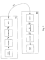
- the communication system drawn in Fig. 1 consists of a transmitter TX, a receiver RX and a transmission line TL.
- the transmitter TX includes a data source DATA SOURCE, an encoder ENCODER, an interleaving device INTERLEAVER and a modulator MOD.
- the receiver RX includes a demodulator DMOD, a de-interleaving device DE-INTERLEAVER, a decoder DECODER and a data sink DATA SINK.
- An output of the transmitter TX is coupled to an input of the receiver RX via the transmission line TL.
- the data source DATA SOURCE, the encoder ENCODER, the interleaver INTERLEAVER and the modulator MOD are cascade connected.
- An output of the modulator MOD is coupled to the transmission line TL via the transmitter output.
- the other end of the transmission line TL is coupled to an input of the demodulator DMOD via the receiver input.
- the demodulator DMOD, the de-interleaver DE-INTERLEAVER, the decoder DECODER and the data sink DATA SINK are cascade connected.
- the data source DATA SOURCE produces a data stream which may comprise user data bytes and/or overhead data bytes. A fixed amount of these bytes constitutes a single word and each one of these words is encoded by the encoder ENCODER. This implies that the encoder ENCODER extends each of the words according to predefined mathematical schemes by adding redundant bytes thereto. These redundant bytes and the mathematical schemes will enable the receiver RX to detect and probably to correct errors in transmitted words.
- the extended words generated by the encoder ENCODER are called codewords and constitute an incoming data stream ID for the interleaver INTERLEAVER.
- the interleaver INTERLEAVER By re-sequencing the data bytes of different codewords of the incoming data stream ID, the interleaver INTERLEAVER produces an outgoing interleaved data stream OID which is better protected for burst noise on the transmission line TL than the incoming data stream ID.
- the modulator MOD finally modulates data symbols, i.e. combinations of data bits of the data stream OID which represent one point in the constellation scheme of the modulation method, on one or more carriers to be transmitted over the transmission line TL.
- the demodulator DMOD demodulates the data symbols from the carrier(s) and generates from the demodulated data symbols a stream of data bytes named the incoming interleaved data stream IID.
- the bytes of the incoming interleaved data stream IID are re-sequenced in the de-interleaver DE-INTERLEAVER so that the effect of the interleaver INTERLEAVER on the order of bytes is compensated for and the generated outgoing data stream OD again contains the original sequence of data bytes.
- the decoder DECODER errors due to transmission are detected and corrected by using the already mentioned mathematical schemes and the information of the redundantly added bytes.
- the so determined data stream then is applied to the data sink DATA SINK, which may be any kind of terminal, interface or the like.
- the interleaver INTERLEAVER and de-interleaver DE-INTERLEAVER are designed to provide to the transmitted data stream a transmit rate independent impulse noise immunity.
- the INTERLEAVER and DE-INTERLEAVER structure which realise this object, is drawn in Fig. 2 and Fig. 3 respectively, and is described in detail in the following paragraphs.
- the interleaver INTERLEAVER of Fig. 2 includes writing means WRITE, reading means READ, a memory MEM, an address generator ADDRESS and a controller CTRL.
- the memory MEM is equipped with a triangular shaped matrix MAT of memory cells wherein each row is constituted by a first-in-first-out queue of memory cells.
- the writing means WRITE, the memory MEM, and the reading means READ are cascade connected between the incoming data input ID and an outgoing interleaved data output OID of the interleaver INTERLEAVER.
- An output of the controller CTRL and a control input CI of the address generator ADDRESS are interconnected and two outputs of the address generator ADDRESS are coupled to address inputs AI1 of the writing means WRITE and AI2 of the reading means READ respectively.
- the writing means WRITE has to store incoming data bytes and from which memory cells the reading means READ has to read outgoing data bytes is defined by the addresses generated by the address generator ADDRESS.
- address generator ADDRESS generates a first sequence of row ordinates or write addresses indicating to which rows of the interleaving matrix MAT subsequent incoming data bytes are to be applied and a second sequence of row ordinates or read addresses indicating from which rows of the interleaving matrix MAT subsequent outgoing data symbols are to be read. How both sequences look like depends upon the state wherein the address generator ADDRESS is set by the controller CTRL. The following paragraphs briefly describe three states wherein the address generator ADDRESS can be set.
- subsequent incoming data bytes are applied to subsequent rows of the matrix MAT in a circular way.
- Subsequent outgoing data bytes are, still during this steady state, read from subsequent rows of the matrix MAT in a circular way. This is realised for instance if the incoming and outgoing rates are equal and a byte is read from each row wherein a byte is written. Since the rows have different lengths, subsequently read data bytes were not subsequently written in the matrix MAT.
- the address generator ADDRESS is set in a transition state during which the interleaving depth is decreased, the number of data bytes read from each row of the matrix MAT is positively linearly related to the ordinate of that row. At the end of this transition state, the increment parameter M is decreased and also the average interleaving delay (the time between entering and leaving the interleaver INTERLEAVER for a single data byte) is decreased.
- the address generator ADDRESS is set in a transition state during which the interleaving depth is increased, the number of data bytes read from each row of the matrix MAT is negatively linearly related to the ordinate of that row. At the end of this transition state, the increment parameter M is increased and also the average interleaving delay is increased.
- the de-interleaver DE-INTERLEAVER of Fig. 3 includes writing means WRITE', reading means READ', a memory MEM', an address generator ADDRESS' and a controller CTRL'.
- the memory MEM' is equipped with a triangular shaped matrix MAT' of memory cells wherein each row is constituted by a first-in-first-out queue of memory cells.
- the writing means WRITE', the memory means MEM', and the reading means READ' are cascade connected between the incoming interleaved data input IID and the outgoing data output OD of the de-interleaver DE-INTERLEAVER.
- An output of the controller CTRL' and a control input CI' of the address generator ADDRESS' are interconnected and two outputs of the address generator ADDRESS' are coupled to address inputs Al1' of the writing means WRITE' and AI2' of the reading means READ' respectively.
- the incoming interleaved data bytes applied to the de-interleaver DE-INTERLEAVER via its incoming interleaved data input IID are written in tail memory cells of the queues of the de-interleaving matrix MAT'. Meanwhile, outgoing data bytes are read out of head memory cells of the queues of the matrix MAT' by the reading means READ' and applied to the outgoing data output OD of the de-interleaver DE-INTERLEAVER.
- memory cells the writing means WRITE' has to write data bytes and from which memory cells the reading means READ' has to deduce data bytes is defined by the addresses generated by the address generator ADDRESS'.
- This address generator ADDRESS' generates a first sequence of row ordinates or write addresses indicating to which rows of the interleaving matrix MAT' subsequent incoming interleaved data bytes are to be applied, and a second sequence of row ordinates or read addresses indicating from which rows of the interleaving matrix MAT' subsequent outgoing data bytes are to be read. How both sequences look like depends upon the state wherein the address generator ADDRESS' is set by the controller CTRL'. The following paragraphs again briefly describe three states wherein the address generator ADDRESS' can be set.
- the address generator ADDRESS' is set in a transition state during which the interleave depth is decreased, the number of data bytes written in each row of the matrix MAT' is positively linearly related to the ordinate of that row.
- the decrement parameter M is decreased and also the average de-interleaving delay (the time between entering and leaving the de-interleaver DE-INTERLEAVER) is decreased.
- the address generator ADDRESS' is set in a transition state during which the interleave depth is increased, the number of data bytes written in each row of the matrix MAT' is negatively linearly related to the ordinate of that row. At the end of this transition state, the decrement parameter M is increased and also the average de-interleaving delay is increased.
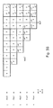
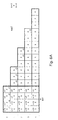
- the address generators, ADDRESS and ADDRESS' are set in the transition state wherein the delay increment parameter M is increased from 3 to 4.
- the filling of MAT and MAT' during this last state is described by referring to Fig. 6A and Fig. 6B.
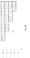
- Fig. 4A the matrix MAT is shown.
- Each row of this matrix MAT is constituted by a first-in-first-out memory, with tail memory cell at the leftmost side and head memory cell at the rightmost side. If a byte is applied to a row of matrix MAT, it is thus stored in the tail memory cell. Before writing this byte in the tail memory cell however, the byte contained by the head memory cell is read and all bytes in the first-in-first-out memory are shifted one position towards the head memory cell.
- a first-in-first-out memory may be realised in hardware (e.g. a shift register) or software (by adapting the tail and head memory cell pointers with a program each time a byte is written or read).
- the write-to-read delay experienced by a byte applied to a row of the matrix MAT is proportional to the length of the first-in-first-out memory constituting that row.
- the matrix drawn in Fig. 4A contains 5 rows with ordinates 0, 1, 2, 3 and 4 and first-in-first-out memories Fifo0, Fifo1, Fifo2, Fifo3 and Fifo4.
- the delay experienced by a byte in MAT is equal to j.M.l.
- j represents the ordinate of the row
- M represents the delay increment per row
- I represents the number of rows in the matrix MAT.
- the de-interleaving matrix MAT' of Fig. 4B is similar to the interleaving matrix MAT of Fig. 4A but the row ordinates are reversed so that row ordinates corresponding to short first-in-first-out memories in the interleaving matrix MAT, correspond to long first-in-first-out memories in the de-interleaving matrix MAT'.
- Subsequent incoming bytes are written in subsequent rows of the matrix MAT.
- the first byte experiences no interleaving delay and is immediately transmitted to the receiver.
- Fifo0 therefore is an empty queue in Fig. 4A.
- the second byte is written in Fifo1 which is indicated by w2 in Fig. 4A.
- the third byte, fourth byte and fifth byte are applied to Fifo2, Fifo3 and Fifo4 respectively and fill the memory cells marked by w3, w4 and w5.
- the sixth byte again passes through Fifo0 and experiences no interleaving delay and bytes 7, 8, 9 and 10 are subsequently stored in the new tail memory cells of Fifo1, Fifo2, Fifo3 and Fifo4 marked by w7, w8, w9 and w10 respectively.
- the first byte is transmitted without interleaving delay, and is followed by bytes r2, r3, r4, r5 read from Fifo1, Fifo2, Fifo3 and Fifo4 respectively.
- a byte is transmitted without interleaving delay and this one is followed by bytes r7, r8, r9 and r10.
- indexes used in Fig. 4B with prefixes w and r in a similar way indicate how the interleaved incoming stream of bytes is stored in the de-interleaving matrix MAT' and read therefrom to constitute the non-interleaved output data stream.
- Fifo4' is an empty queue which indicates that bytes applied to this row experience no de-interleaving delay.
- the interleaving depth D is equal to I*M+1.
- I again represents the number of rows in the interleaving matrix MAT.
- the interleave depth D also has to increase to keep constant impulse noise immunity. This can again be realised by manipulating M and the structure of the matrices MAT and MAT'. The following paragraphs will clarify how M can be increased from 3 to 4 during the transition state illustrated by Fig. 6A and Fig. 6B.
- the transition phase to increase M from 3 to 4 is initiated by filling a buffer BUF of l.(l-1) bytes in the interleaver. Afterwards, following sequence of bytes is transmitted:
- any connection between the transmitter TX and receiver RX e.g. a cable connection, a telephone line, a satellite connection, an optical fibre, a radio link through the air, and so on may be affected by burst noise and can thus be protected by a method according to the present invention.
- the present invention is very suitable for being used in VSDL (Very High Speed Digital Subscriber Line) modems or the like. These modems will transport digital data at high bitrates over telephone lines.
- the telephone lines may be affected by several sources of burst noise, especially when the lines are stretched through the air. Radio interference from radio amateurs, critical weather conditions, transient appearances due to ringing and hooking are a few of the noise sources affecting transmission over such telephone lines.
- the present invention is an attractive solution for providing transmit rate independent impulse noise immunity in such VSDL systems, the applicability of the present invention is not limited to these systems or to similar systems having the same type of modulation and/or encoding.
- the modulation constellation and encoding scheme used by the modulator and the encoder respectively are of no importance for the present invention.
- the transmitter TX and receiver RX may be integrated in a single transceiver. This is so in modems which are adapted to transmit and receive data to and from a bidirectional transmission line.
- the triangular interleaving and de-interleaving matrixes, MAT and MAT' may be grouped to constitute a rectangular interleaving/de-interleaving matrix.
- both writing means WRITE and WRITE'
- both reading means READ and READ'
- both addressing means ADDRESS and ADDRESS'
- controllers CTRL and CTRL'
- the delay increment parameter M may be increased or decreased by more than one unit. As well for the decreasing as for the increasing process, it suffices to execute the above described transition states more than once.
Landscapes
- Engineering & Computer Science (AREA)
- Theoretical Computer Science (AREA)
- Physics & Mathematics (AREA)
- Probability & Statistics with Applications (AREA)
- Quality & Reliability (AREA)
- General Engineering & Computer Science (AREA)
- General Physics & Mathematics (AREA)
- Error Detection And Correction (AREA)
- Detection And Prevention Of Errors In Transmission (AREA)
- Communication Control (AREA)
- Signal Processing For Digital Recording And Reproducing (AREA)
Claims (12)
- Verfahren zur Verschachtelung eintreffender Datenbytes (w1, ..., w10) eines eintreffenden Datenstroms (ID), um dadurch einen abgehenden verschachtelten Datenstrom (OID) mit abgehenden verschachtelten Datenbytes (r1, ..., r10) zu erzeugen, wobei die eintreffenden Datenbytes (w1, ..., w10) in hinten liegende Speicherzellen von Zeilen einer dreieckigen Matrix (MAT) von Speicherzellen geschrieben werden, worin jede Zeile von Speicherzellen in der Matrix (MAT) eine First-In-First-Out-Warteschlange (Fifo0, Fifo1, Fifo2, Fifo3, Fifo4) repräsentiert und worin die abgehenden verschachtelten Datenbytes (r1, ..., r10) aus vorne liegenden Speicherzellen der Zeilen ausgelesen werden und dadurch der abgehende verschachtelte Datenstrom (OID) realisiert wird,
DADURCH GEKENNZEICHNET, DASS, wenn sich die Übertragungsrate für die Übertragung des abgehenden verschachtelten Datenstroms (OID) erhöht oder verringert, aus jeder Zeile eine Anzahl der abgehenden verschachtelten Datenbytes (r1, ..., r10) ausgelesen wird, die negativ, bzw. positiv linear mit einer Ordinaten-Nummer (0, 1, 2, 3, 4) der Zeile in der dreieckigen Matrix (MAT) verknüpft ist, wobei in der Zwischenzeit eine gleiche Anzahl von eintreffenden Datenbytes (w1, ..., w10) in jede Zeile der dreieckigen Matrix geschrieben wird. - Verfahren zur Verschachtelung gemäß Anspruch 1,
DADURCH GEKENNZEICHNET, DASS, wenn die Übertragungsrate sinkt, aufeinander folgende abgehende verschachtelte Datenbytes (r1, ..., r10) ausgelesen werden aus:und so weiter, bis abgehende verschachtelte Datenbytes aus Zeile 1 bis Zeile 1-1 ausgelesen sind, wobei 1 die Anzahl von Zeilen in der dreieckigen Matrix (MAT) ist.Zeile 1;Zeile 1-1 und Zeile 1;Zeile 1-2, Zeile 1-1 und Zeile 1, - Verfahren zur Verschachtelung gemäß Anspruch 2,
DADURCH GEKENNZEICHNET, DASSund so weiter.1-1 Leer-Bytes erzeugt und in den abgehenden verschachtelten Datenstrom (OID) eingefügt werden, bevor ein erstes abgehendes verschachteltes Datenbyte aus Zeile 1 ausgelesen wird;1-2 Leer-Bytes erzeugt und in den abgehenden verschachtelten Datenstrom (OID) eingefügt werden, bevor ein erstes abgehendes verschachteltes Datenbyte aus Zeile 1-1 ausgelesen wird;1-3 Leer-Bytes erzeugt und in den abgehenden verschachtelten Datenstrom (OID) eingefügt werden, bevor ein erstes abgehendes verschachteltes Datenbyte aus Zeile 1-2 ausgelesen wird, - Verfahren zur Verschachtelung gemäß Anspruch 1,
DADURCH GEKENNZEICHNET, DASS, wenn die Übertragungsrate steigt, aufeinander folgende abgehende verschachtelte Datenbytes (r1, ..., r10) ausgelesen werden aus:und so weiter, bis abgehende verschachtelte Datenbytes aus Zeile 0 bis Zeile 1-2 ausgelesen sind, wobei 1 die Anzahl von Zeilen in der dreieckigen Matrix (MAT) ist.Zeile 0;Zeile 0 und Zeile 1;Zeile 0, Zeile 1 und Zeile 2, - Verfahren zur Verschachtelung gemäß Anspruch 4,
DADURCH GEKENNZEICHNET, DASSund so weiter.1-1 Leer-Bytes erzeugt und in den abgehenden verschachtelten Datenstrom (OID) eingefügt werden, nachdem ein erstes abgehendes verschachteltes Datenbyte aus Zeile 0 ausgelesen wird;1-2 Leer-Bytes erzeugt und in den abgehenden verschachtelten Datenstrom (OID) eingefügt werden, nachdem ein erstes abgehendes verschachteltes Datenbyte aus Zeile 1 ausgelesen wird;1-3 Leer-Bytes erzeugt und in den abgehenden verschachtelten Datenstrom (OID) eingefügt werden, nachdem ein erstes abgehendes verschachteltes Datenbyte aus Zeile 2 ausgelesen wird, - Verfahren zur Entschachtelung eintreffender verschachtelter Datenbytes (w1', ..., w10') eines eintreffenden verschachtelten Datenstroms (IID), um dadurch einen abgehenden Datenstrom (OD) mit abgehenden Datenbytes (r1', ..., r10') zu erzeugen, wobei die eintreffenden verschachtelten Datenbytes (w1', ..., w10') in hinten liegende Speicherzellen von Zeilen einer dreieckigen Matrix (MAT') von Speicherzellen geschrieben werden, worin jede Zeile von Speicherzellen in der Matrix (MAT') eine First-In-First-Out-Warteschlange (Fifo0', Fifo1', Fifo2', Fifo3', Fifo4') repräsentiert und worin die abgehenden Datenbytes (r1', ..., r10') aus vorne liegenden Speicherzellen der Zeilen ausgelesen werden und dadurch der abgehende Datenstrom (OD) realisiert wird,
DADURCH GEKENNZEICHNET, DASS, wenn sich die Übertragungsrate für die Übertragung des eintreffenden verschachtelten Datenstroms (IID) erhöht oder verringert, in jede Zeile der dreieckigen Matrix (MAT') eine Anzahl der eintreffenden verschachtelten Datenbytes (w1', ..., w10') geschrieben wird, die negativ, bzw. positiv linear mit einer Ordinaten-Nummer (0, 1, 2, 3, 4) der Zeile in der dreieckigen Matrix (MAT') verknüpft ist, wobei in der Zwischenzeit eine gleiche Anzahl von abgehenden Datenbytes (r1', ..., r10') aus jeder Zeile der dreieckigen Matrix (MAT') gelesen wird. - Verschachtelungs-Vorrichtung (INTERLEAVER), die dazu verwendet wird, die Reihenfolge eintreffender Datenbytes (w1, ..., w10) eines eintreffenden Datenstroms (ID) zu ändern, um dadurch einen abgehenden verschachtelten Datenstrom (OID) aus abgehenden verschachtelten Datenbytes (r1, ..., r10) zu erzeugen, wobei die Verschachtelungs-Vorrichtung (INTERLEAVER) folgendes umfasst:DADURCH GEKENNZEICHNET, DASS die Adresserzeugungs-Mittel (ADDRESS) weiterhin so angepasst sind, dass sie, wenn sich die Übertragungsrate für die Übertragung des abgehenden verschachtelten Datenstroms (OID) erhöht oder verringert, für jede Zeile eine Anzahl von Leseadressen erzeugen, die negativ, bzw. positiv linear mit einer Ordinaten-Nummer (0, 1, 2, 3, 4) der Zeile in der dreieckigen Matrix (MAT) verknüpft ist, und in der Zwischenzeit eine gleich große Anzahl von Schreibadressen für jede Zeile der dreieckigen Matrix (MAT) erzeugen.a. Speicher-Mittel (MEM), die eine Vielzahl von First-In-First-Out-Warteschlangen (Fifo0, Fifo1, Fifo2, Fifo3, Fifo4) enthalten, die so angepasst sind, dass sie entsprechende Zeilen einer dreieckigen Matrix (MAT) von Speicherzellen repräsentieren;b. Schreib-Mittel (WRITE) mit einem Ausgang, der mit einem Eingang der Speicher-Mittel (MEM) gekoppelt ist, wobei die Schreib-Mittel (WRITE) so angepasst sind, dass sie jedes der eintreffenden Datenbytes (w1, ..., w10) in eine hinten liegende Speicherzelle einer der Zeilen schreiben, die durch eine Schreibadresse gekennzeichnet wird;c. Lese-Mittel (READ) mit einem Eingang, der mit einem Ausgang der Speicher-Mittel (MEM) gekoppelt ist, wobei die Lese-Mittel (READ) so angepasst sind, dass sie jedes der abgehenden verschachtelten Datenbytes (r1, ..., r10) aus einer vorne liegenden Speicherzelle einer der Zeilen lesen, die durch eine Leseadresse gekennzeichnet wird; undd. Adresserzeugungs-Mittel (ADDRESS), von denen ein erster Ausgang mit einem Adress-Eingang (AI1) der Schreib-Mittel (WRITE) gekoppelt ist und von denen ein zweiter Ausgang mit einem Adress-Eingang (AI2) der Lese-Mittel (READ) gekoppelt ist, wobei die Adresserzeugungs-Mittel (ADDRESS) so angepasst sind, dass sie die Schreibadresse und die Leseadresse erzeugen,
- Verschachtelungs-Vorrichtung (INTERLEAVER) gemäß Anspruch 7,
DADURCH GEKENNZEICHNET, DASS die Verschachtelungs-Vorrichtung (INTERLEAVER) weiterhin folgendes enthält:e. Steuerungs-Mittel (CTRL), von denen ein Ausgang mit einem Steuerungs-Eingang (CI) der Adresserzeugungs-Mittel (ADDRESS) gekoppelt ist, wobei die Steuerungs-Mittel (CTRL) so angepasst sind, dass sie die Adresserzeugungs-Mittel (ADDRESS) entweder in einen stabilen Zustand oder in einen Übergangszustand bringen, und weiterhin dadurch, dassf. das Adresserzeugungs-Mittel (ADDRESS) so angepasst ist, die Leseadressen auf diese Weise im Übergangszustand zu erzeugen, und so angepasst ist, im stabilen Zustand für jede Zeile der dreieckigen Matrix (MAT) eine gleiche Anzahl von Leseadressen zu erzeugen und in der Zwischenzeit für jede Zeile eine gleiche Anzahl von Schreibadressen zu erzeugen. - Verschachtelungs-Vorrichtung (INTERLEAVER) gemäß Anspruch 7,
DADURCH GEKENNZEICHNET, DASS das Speicher-Mittel (MEM) weiterhin folgendes enthält:g. Einen Puffer von höchstens 1*(1-1) Speicherzellen, wobei 1 die Anzahl der Zeilen in der dreieckigen Matrix (MAT) ist, und wobei der Puffer so angepasst ist, vorübergehend einen Teil der eintreffenden Datenbytes (w1, ..., w10) zu speichern. - Entschachtelungs-Vorrichtung (DE-INTERLEAVER), die dazu verwendet wird, die Reihenfolge eintreffender verschachtelter Datenbytes (w1', ..., w10') eines eintreffenden verschachtelten Datenstroms (IID) zu ändern, um dadurch einen abgehenden Datenstrom (OD) aus abgehenden Datenbytes (r1', ..., r10') zu erzeugen, wobei die Entschachtelungs-Vorrichtung (DE-INTERLEAVER) folgendes umfasst:a. Speicher-Mittel (MEM'), die eine Vielzahl von First-In-First-Out-Warteschlangen (Fifo0', Fifo1', Fifo2', Fifo3', Fifo4') enthalten, die so angepasst sind, dass sie entsprechende Zeilen einer dreieckigen Matrix (MAT) von Speicherzellen repräsentieren;b. Schreib-Mittel (WRITE') mit einem Ausgang, der mit einem Eingang der Speicher-Mittel (MEM') gekoppelt ist, wobei die Schreib-Mittel (WRITE') so angepasst sind, dass sie jedes der eintreffenden verschachtelten Datenbytes (w1', ..., w10') in eine hinten liegende Speicherzelle einer der Zeilen schreiben, die durch eine Schreibadresse gekennzeichnet wird;c. Lese-Mittel (READ') mit einem Eingang, der mit einem Ausgang der Speicher-Mittel (MEM') gekoppelt ist, wobei die Lese-Mittel (READ') so angepasst sind, dass sie jedes der abgehenden Datenbytes (r1', ..., r10') aus einer vorne liegenden Speicherzelle einer der Zeilen lesen, die durch eine Leseadresse gekennzeichnet wird; undd. Adresserzeugungs-Mittel (ADDRESS'), von denen ein erster Ausgang mit einem Adress-Eingang (AI1') der Schreib-Mittel (WRITE') gekoppelt ist und von denen ein zweiter Ausgang mit einem Adress-Eingang (AI2') der Lese-Mittel (READ') gekoppelt ist, wobei die Adresserzeugungs-Mittel (ADDRESS') so angepasst sind, dass sie die Schreibadresse und die Leseadresse erzeugen,
DADURCH GEKENNZEICHNET, DASS die Adresserzeugungs-Mittel (ADDRESS') weiterhin so angepasst sind, dass sie, wenn sich die Übertragungsrate für die Übertragung des eintreffenden verschachtelten Datenstroms (IID) erhöht oder verringert, für jede Zeile der dreieckigen Matrix (MAT') eine Anzahl von Schreibadressen erzeugen, die negativ, bzw. positiv linear mit einer Ordinaten-Nummer (0, 1, 2, 3, 4) der Zeile in der dreieckigen Matrix (MAT') verknüpft ist, und in der Zwischenzeit eine gleich große Anzahl von Leseadressen für jede Zeile der dreieckigen Matrix (MAT') erzeugen. - Entschachtelungs-Vorrichtung (DE-INTERLEAVER) gemäß Anspruch 10,
DADURCH GEKENNZEICHNET, DASS die Entschachtelungs-Vorrichtung (DE-INTERLEAVER) weiterhin folgendes enthält:e. Steuerungs-Mittel (CTRL'), von denen ein Ausgang mit einem Steuerungs-Eingang (CI') der Adresserzeugungs-Mittel (ADDRESS') gekoppelt ist, wobei die Steuerungs-Mittel (CTRL') so angepasst sind, dass sie die Adresserzeugungs-Mittel (ADDRESS') entweder in einen stabilen Zustand oder in einen Übergangszustand bringen, und weiterhin dadurch, dassf. das Adresserzeugungs-Mittel (ADDRESS') so angepasst ist, die Schreibadressen auf diese Weise im Übergangszustand zu erzeugen, und so angepasst ist, im stabilen Zustand für jede Zeile der dreieckigen Matrix (MAT') eine gleiche Anzahl von Leseadressen zu erzeugen und in der Zwischenzeit für jede Zeile eine gleiche Anzahl von Schreibadressen zu erzeugen. - Entschachtelungs-Vorrichtung (DE-INTERLEAVER) gemäß Anspruch 10,
DADURCH GEKENNZEICHNET, DASS das Speicher-Mittel (MEM') weiterhin folgendes enthält:g. Einen Puffer von höchstens 1*(l-1)/2 Speicherzellen, wobei 1 die Anzahl der Zeilen in der dreieckigen Matrix (MAT') ist, und wobei der Puffer so angepasst ist, vorübergehend einen Teil der eintreffenden verschachtelten Datenbytes (w1', ..., w10') zu speichern.
Priority Applications (10)
| Application Number | Priority Date | Filing Date | Title |
|---|---|---|---|
| AT97400231T ATE292336T1 (de) | 1997-01-31 | 1997-01-31 | Verfahren und geräte zur schachtelung/entschachtelung von digitalen daten und kommunikationssystem |
| DE69732896T DE69732896T2 (de) | 1997-01-31 | 1997-01-31 | Verfahren und Geräte zur Schachtelung/Entschachtelung von digitalen Daten und Kommunikationssystem |
| ES97400231T ES2236784T3 (es) | 1997-01-31 | 1997-01-31 | Metodo y dispositivo para intercalar y desintercalar datos digitales y sistema de comunicacion. |
| EP97400231A EP0856949B1 (de) | 1997-01-31 | 1997-01-31 | Verfahren und Geräte zur Schachtelung/Entschachtelung von digitalen Daten und Kommunikationssystem |
| IL12298298A IL122982A (en) | 1997-01-31 | 1998-01-19 | Interleaving and de-interleaving method for digital data, interleaving and de-interleaving devices, and communication system |
| US09/010,814 US6151690A (en) | 1997-01-31 | 1998-01-23 | Interleaving and de-interleaving method for digital data, interleaving and de-interleaving devices, and communication system |
| AU52730/98A AU726761B2 (en) | 1997-01-31 | 1998-01-23 | Interleaving and de-interleaving method for digital data |
| CA002225058A CA2225058A1 (en) | 1997-01-31 | 1998-01-27 | Interleaving and de-interleaving method for digital data, interleaving and de-interleaving devices, and communication system |
| JP01950098A JP4049429B2 (ja) | 1997-01-31 | 1998-01-30 | デジタルデータ用のインタリーブ方法およびインタリーブ解除方法、インタリーブ装置およびインタリーブ解除装置および通信システム |
| KR10-1998-0002661A KR100502384B1 (ko) | 1997-01-31 | 1998-01-31 | 디지털데이타의인터리브및역인터리브방법,인터리브및역인터리브장치,및통신시스템 |
Applications Claiming Priority (1)
| Application Number | Priority Date | Filing Date | Title |
|---|---|---|---|
| EP97400231A EP0856949B1 (de) | 1997-01-31 | 1997-01-31 | Verfahren und Geräte zur Schachtelung/Entschachtelung von digitalen Daten und Kommunikationssystem |
Publications (2)
| Publication Number | Publication Date |
|---|---|
| EP0856949A1 EP0856949A1 (de) | 1998-08-05 |
| EP0856949B1 true EP0856949B1 (de) | 2005-03-30 |
Family
ID=8229705
Family Applications (1)
| Application Number | Title | Priority Date | Filing Date |
|---|---|---|---|
| EP97400231A Expired - Lifetime EP0856949B1 (de) | 1997-01-31 | 1997-01-31 | Verfahren und Geräte zur Schachtelung/Entschachtelung von digitalen Daten und Kommunikationssystem |
Country Status (10)
| Country | Link |
|---|---|
| US (1) | US6151690A (de) |
| EP (1) | EP0856949B1 (de) |
| JP (1) | JP4049429B2 (de) |
| KR (1) | KR100502384B1 (de) |
| AT (1) | ATE292336T1 (de) |
| AU (1) | AU726761B2 (de) |
| CA (1) | CA2225058A1 (de) |
| DE (1) | DE69732896T2 (de) |
| ES (1) | ES2236784T3 (de) |
| IL (1) | IL122982A (de) |
Cited By (1)
| Publication number | Priority date | Publication date | Assignee | Title |
|---|---|---|---|---|
| US7657818B2 (en) | 2005-06-22 | 2010-02-02 | Adaptive Spectrum And Signal Alignment, Inc. | Dynamic minimum-memory interleaving |
Families Citing this family (55)
| Publication number | Priority date | Publication date | Assignee | Title |
|---|---|---|---|---|
| US6055277A (en) * | 1997-05-29 | 2000-04-25 | Trw Docket No. | Communication system for broadcasting to mobile users |
| GB2332836A (en) * | 1997-12-24 | 1999-06-30 | Daewoo Electronics Co Ltd | Adaptive convolutional interleaver and deinterleaver |
| US6507629B1 (en) * | 1998-04-07 | 2003-01-14 | Sony Corporation | Address generator, interleave unit, deinterleave unit, and transmission unit |
| EP1017175B1 (de) * | 1998-05-27 | 2007-07-18 | Ntt Mobile Communications Network Inc. | Verfahren und Vorrichtung zum Verchachteln einer ersten Bitsequenz in eine zweite Bitsequenz |
| JP3359291B2 (ja) * | 1998-07-17 | 2002-12-24 | 株式会社ケンウッド | デインターリーブ回路 |
| US6347385B1 (en) * | 1998-08-03 | 2002-02-12 | Nortel Networks Limited | Interleavers for turbo code |
| US6381728B1 (en) * | 1998-08-14 | 2002-04-30 | Qualcomm Incorporated | Partitioned interleaver memory for map decoder |
| GB2343342A (en) * | 1998-10-28 | 2000-05-03 | Int Mobile Satellite Org | Satellite communication system with variable data transmission rate |
| US6536001B1 (en) * | 1999-03-11 | 2003-03-18 | Globespanvirata, Inc. | Circuit and method for convolutional interleaving using a single modulo operation |
| AU4207800A (en) * | 1999-04-09 | 2000-11-14 | Sony Electronics Inc. | Interleavers and de-interleavers |
| KR100526512B1 (ko) * | 1999-05-20 | 2005-11-08 | 삼성전자주식회사 | 이동 통신시스템의 직렬 쇄상 컨볼루션 부호화를 위한 인터리빙장치 및 방법 |
| US7088781B2 (en) * | 1999-12-15 | 2006-08-08 | Paradyne Corporation | Tone ordered discrete multitone interleaver |
| US6823002B1 (en) * | 1999-12-15 | 2004-11-23 | Paradyne Corporation | Linear block interleaver for discrete multi-tone modulation |
| US7099401B2 (en) * | 1999-12-15 | 2006-08-29 | Paradyne Corporation | Discrete multitone interleaver |
| US6971057B1 (en) * | 2000-02-25 | 2005-11-29 | Globespanvirata, Inc. | System and method for efficient convolutional interleaving/de-interleaving |
| US6634009B1 (en) * | 2000-03-08 | 2003-10-14 | Altera Corporation | Interleaver-deinterleaver megacore |
| FR2812150A1 (fr) * | 2000-07-18 | 2002-01-25 | St Microelectronics Sa | Dispositif d'emission/reception de donnees numeriques capable de traiter des debits differents, en particulier dans un environnement vdsl |
| GB2369274A (en) * | 2000-11-17 | 2002-05-22 | Ubinetics Ltd | Interleaving by data permutation without a matrix |
| US6981031B2 (en) * | 2000-12-15 | 2005-12-27 | International Business Machines Corporation | Language independent message management for multi-node application systems |
| JP4336809B2 (ja) * | 2001-02-16 | 2009-09-30 | 日本電気株式会社 | インタリーブ方法 |
| US7385949B1 (en) | 2001-06-05 | 2008-06-10 | Broadcom Corporation | System and method for de-interleaving data in a wireless receiver |
| US6772377B2 (en) * | 2001-09-28 | 2004-08-03 | Texas Instruments Incorporated | Convolutional interleaving with interleave depth larger than codeword size |
| US7024596B2 (en) * | 2001-11-12 | 2006-04-04 | Broadcom Corporation | Efficient address generation for interleaver and de-interleaver |
| US6954832B2 (en) * | 2002-05-31 | 2005-10-11 | Broadcom Corporation | Interleaver for iterative decoder |
| US7433429B2 (en) * | 2002-07-19 | 2008-10-07 | Intel Corporation | De-interleaver method and system |
| US7069398B2 (en) * | 2003-06-20 | 2006-06-27 | Industrial Technology Research Institute | Apparatus and method for de-interleaving the interleaved data in a coded orthogonal frequency division multiplexing receiver |
| FR2857178B1 (fr) * | 2003-07-04 | 2005-09-30 | St Microelectronics Sa | Entrelaceur et dispositif de decodage de signaux numeriques comportant un tel entrelaceur |
| US8077743B2 (en) * | 2003-11-18 | 2011-12-13 | Qualcomm Incorporated | Method and apparatus for offset interleaving of vocoder frames |
| DE102004026800B4 (de) * | 2004-05-24 | 2006-05-24 | Infineon Technologies Ag | Verfahren zum Verändern einer Tiefe einer Interleaver-Vorrichtung oder Deinterleaver-Vorrichtung sowie entsprechende Interleaver-Vorrichtung, Deinterleaver-Vorrichtung und Kommunikationseinrichtung |
| TWI261169B (en) * | 2004-06-11 | 2006-09-01 | Via Tech Inc | Memory size allocation device and method applying in interleaving |
| EP1633052A1 (de) * | 2004-09-07 | 2006-03-08 | STMicroelectronics N.V. | Blocksunverschachtelungssystem |
| CN1750577B (zh) * | 2004-09-17 | 2010-06-16 | 中兴通讯股份有限公司 | 一种实现多路交织和解交织的方法和装置 |
| US7831890B2 (en) | 2004-10-12 | 2010-11-09 | Aware, Inc. | Resource sharing in a telecommunications environment |
| EP1919085A3 (de) | 2004-11-16 | 2008-05-21 | Infineon Technologies AG | Nahtloser Wechsel der Tiefe eines allgemeinen Faltungsverschachtelers während der Übertragung ohne Datenverlust |
| US7529984B2 (en) * | 2004-11-16 | 2009-05-05 | Infineon Technologies Ag | Seamless change of depth of a general convolutional interleaver during transmission without loss of data |
| US7716563B2 (en) * | 2004-11-30 | 2010-05-11 | Ciena Corporation | Method and apparatus for the efficient implementation of a totally general convolutional interleaver in DMT-based xDSL systems |
| US7408999B2 (en) * | 2004-12-09 | 2008-08-05 | Conexant Systems, Inc. | Method and system for dynamic interleaver adaptation scheme in VDSL |
| US8335956B2 (en) | 2006-04-12 | 2012-12-18 | Tq Delta, Llc | Packet retransmission and memory sharing |
| US7865796B2 (en) * | 2006-09-25 | 2011-01-04 | Broadcom Corporation | Method and system for memory partitioning |
| US7751514B2 (en) * | 2007-05-23 | 2010-07-06 | Mediatek Inc. | System and method of detecting burst noise and minimizing the effect of burst noise |
| CN101610089B (zh) * | 2008-06-17 | 2013-06-05 | 中兴通讯股份有限公司 | 一种第二次交织及解交织的方法和装置 |
| CN101547064B (zh) * | 2009-05-06 | 2011-11-09 | 普天信息技术研究院有限公司 | 一种交织速率匹配和解交织解速率匹配方法 |
| US8189408B2 (en) * | 2009-11-17 | 2012-05-29 | Freescale Semiconductor, Inc. | Memory device having shifting capability and method thereof |
| GB2512600A (en) | 2013-04-02 | 2014-10-08 | Sony Corp | Receivers and methods for receiving signals |
| GB2512601B (en) * | 2013-04-02 | 2016-02-10 | Sony Corp | Transmitters and methods for transmitting signals |
| CN103490855B (zh) * | 2013-09-09 | 2017-03-08 | 华为技术有限公司 | 传输信息的方法和装置 |
| KR102265052B1 (ko) | 2014-12-17 | 2021-06-15 | 삼성전자주식회사 | 적응적으로 인터리빙 깊이를 결정하는 인터리빙 방법 및 장치 |
| KR101579194B1 (ko) * | 2015-02-09 | 2015-12-21 | 성균관대학교산학협력단 | 메모리 액세스 방법 및 메모리 장치 |
| US10201026B1 (en) | 2016-06-30 | 2019-02-05 | Acacia Communications, Inc. | Forward error correction systems and methods |
| US11233529B2 (en) | 2017-03-24 | 2022-01-25 | Apple Inc. | Techniques for employing polar code in connection with NR (new radio) |
| WO2018187902A1 (en) | 2017-04-10 | 2018-10-18 | Qualcomm Incorporated | An efficient interleaver design for polar codes |
| CN109150198B (zh) | 2017-06-16 | 2021-05-14 | 华为技术有限公司 | 一种极化码的交织处理方法及装置 |
| KR20240147704A (ko) * | 2017-08-04 | 2024-10-08 | 퀄컴 인코포레이티드 | 폴라 코드를 위한 효율적인 인터리버 설계 |
| US10505676B1 (en) * | 2018-08-10 | 2019-12-10 | Acacia Communications, Inc. | System, method, and apparatus for interleaving data |
| EP3699767B1 (de) * | 2019-02-21 | 2025-02-19 | Realtek Semiconductor Corp. | Vorrichtung und verfahren zur handhabung eines zeitentschachtelerblocks |
Family Cites Families (11)
| Publication number | Priority date | Publication date | Assignee | Title |
|---|---|---|---|---|
| JPS5555412A (en) * | 1978-10-17 | 1980-04-23 | Victor Co Of Japan Ltd | Signal recording and reproducing device |
| JPS5753806A (en) * | 1980-09-16 | 1982-03-31 | Toshiba Corp | Processor of digital signal |
| US4394642A (en) * | 1981-09-21 | 1983-07-19 | Sperry Corporation | Apparatus for interleaving and de-interleaving data |
| US4559625A (en) | 1983-07-28 | 1985-12-17 | Cyclotomics, Inc. | Interleavers for digital communications |
| FR2592258B1 (fr) * | 1985-12-23 | 1991-05-03 | Thomson Csf | Procede et dispositif de transmission radioelectrique d'informations codees, resistant au brouillage |
| FR2693062B1 (fr) * | 1992-06-26 | 1994-09-23 | France Telecom | Procédé et dispositif égaliseur à retour de décisions pour la transmission par blocs de symboles d'information. |
| JP3249280B2 (ja) * | 1994-01-11 | 2002-01-21 | 富士通株式会社 | インターリーブ回路 |
| US5537420A (en) * | 1994-05-04 | 1996-07-16 | General Instrument Corporation Of Delaware | Convolutional interleaver with reduced memory requirements and address generator therefor |
| JPH08335887A (ja) * | 1995-06-08 | 1996-12-17 | Fujitsu Ltd | 複数インタリーブ・マトリクスのインタリーブアドレス生成回路 |
| KR100192797B1 (ko) * | 1996-07-01 | 1999-06-15 | 전주범 | 정적 램을 이용한 길쌈인터리버의 구조 |
| US6055277A (en) * | 1997-05-29 | 2000-04-25 | Trw Docket No. | Communication system for broadcasting to mobile users |
-
1997
- 1997-01-31 EP EP97400231A patent/EP0856949B1/de not_active Expired - Lifetime
- 1997-01-31 ES ES97400231T patent/ES2236784T3/es not_active Expired - Lifetime
- 1997-01-31 DE DE69732896T patent/DE69732896T2/de not_active Expired - Lifetime
- 1997-01-31 AT AT97400231T patent/ATE292336T1/de not_active IP Right Cessation
-
1998
- 1998-01-19 IL IL12298298A patent/IL122982A/xx not_active IP Right Cessation
- 1998-01-23 US US09/010,814 patent/US6151690A/en not_active Expired - Lifetime
- 1998-01-23 AU AU52730/98A patent/AU726761B2/en not_active Expired
- 1998-01-27 CA CA002225058A patent/CA2225058A1/en not_active Abandoned
- 1998-01-30 JP JP01950098A patent/JP4049429B2/ja not_active Expired - Lifetime
- 1998-01-31 KR KR10-1998-0002661A patent/KR100502384B1/ko not_active Expired - Lifetime
Cited By (1)
| Publication number | Priority date | Publication date | Assignee | Title |
|---|---|---|---|---|
| US7657818B2 (en) | 2005-06-22 | 2010-02-02 | Adaptive Spectrum And Signal Alignment, Inc. | Dynamic minimum-memory interleaving |
Also Published As
| Publication number | Publication date |
|---|---|
| DE69732896D1 (de) | 2005-05-04 |
| EP0856949A1 (de) | 1998-08-05 |
| KR19980070970A (ko) | 1998-10-26 |
| JPH10224236A (ja) | 1998-08-21 |
| IL122982A0 (en) | 1998-08-16 |
| DE69732896T2 (de) | 2006-05-11 |
| JP4049429B2 (ja) | 2008-02-20 |
| AU5273098A (en) | 1998-08-06 |
| CA2225058A1 (en) | 1998-07-31 |
| US6151690A (en) | 2000-11-21 |
| IL122982A (en) | 2003-04-10 |
| ES2236784T3 (es) | 2005-07-16 |
| ATE292336T1 (de) | 2005-04-15 |
| KR100502384B1 (ko) | 2005-09-26 |
| AU726761B2 (en) | 2000-11-23 |
Similar Documents
| Publication | Publication Date | Title |
|---|---|---|
| US6151690A (en) | Interleaving and de-interleaving method for digital data, interleaving and de-interleaving devices, and communication system | |
| US5751741A (en) | Rate-adapted communication system and method for efficient buffer utilization thereof | |
| US5742612A (en) | Method and device for interleaving a sequence of data elements | |
| US5983388A (en) | Forward error correction arrangement (FEC) for multipoint to single point communication systems | |
| US6683855B1 (en) | Forward error correction for high speed optical transmission systems | |
| JP3274627B2 (ja) | 入力信号のストリームを符号化する方法と出力信号ストリームを生成する方法 | |
| US8351537B2 (en) | Seamless change of depth of a general convolutional interleaver during transmission without loss of data | |
| KR100852083B1 (ko) | 인코딩된 인터리빙 신호의 복조 및 디코딩 방법과 그를수신하는 수신기 | |
| US5010553A (en) | High speed, error-free data transmission system and method | |
| JP3748550B2 (ja) | 高速ダウンリンクパケットアクセス移動通信システムにおけるシンボルマッピングのためのインターリービング装置及び方法 | |
| EP0833474A2 (de) | Verfahren und Vorrichtung zum Verschachteln von Daten in einem Sender für asymmetrische digitale Teilnehmerleitungen (ADSL) | |
| US8621316B2 (en) | Method and device for encoding of error correcting codes, and method and device for decoding of error correcting codes | |
| KR20040014977A (ko) | 강화한 코딩 스킴들을 사용하는 디지털 텔레비전 전송시스템 | |
| US5928371A (en) | Systems for programmably interleaving and de-interleaving data and method thereof | |
| JP2003023373A (ja) | 符号分割多重接続移動通信システムでのデータ送/受信装置及び方法 | |
| US12224770B2 (en) | Receiver receiving a signal including physical layer frames, and including a convolutional deinterleaver and a deinterleaver selector | |
| US7408999B2 (en) | Method and system for dynamic interleaver adaptation scheme in VDSL | |
| US20080092009A1 (en) | Error Correction Coding Apparatus and Error Correction Decoding Apparatus | |
| US6772377B2 (en) | Convolutional interleaving with interleave depth larger than codeword size | |
| EP0892501A1 (de) | Faltungsverschachteler und Faltungsentschachteler | |
| US4159469A (en) | Method and apparatus for the coding and decoding of digital information | |
| US6329935B1 (en) | Temporally separating and re-organizing data using two-stage interleaving and de-interleaving | |
| US7577881B1 (en) | Method and apparatus for an interleaver | |
| CA2303630A1 (en) | A system and method for forward error correction | |
| US20020083248A1 (en) | Interleave circuit, de-interleave circuit and xDSL modem |
Legal Events
| Date | Code | Title | Description |
|---|---|---|---|
| PUAI | Public reference made under article 153(3) epc to a published international application that has entered the european phase |
Free format text: ORIGINAL CODE: 0009012 |
|
| AK | Designated contracting states |
Kind code of ref document: A1 Designated state(s): AT BE CH DE DK ES FI FR GB GR IE IT LI LU MC NL PT SE |
|
| RAP3 | Party data changed (applicant data changed or rights of an application transferred) |
Owner name: ALCATEL |
|
| RAP3 | Party data changed (applicant data changed or rights of an application transferred) |
Owner name: ALCATEL |
|
| 17P | Request for examination filed |
Effective date: 19990205 |
|
| AKX | Designation fees paid |
Free format text: AT BE CH DE DK ES FI FR GB GR IE IT LI LU MC NL PT SE |
|
| RBV | Designated contracting states (corrected) |
Designated state(s): AT BE CH DE DK ES FI FR GB GR IE IT LI LU MC NL PT SE |
|
| 17Q | First examination report despatched |
Effective date: 20021030 |
|
| GRAP | Despatch of communication of intention to grant a patent |
Free format text: ORIGINAL CODE: EPIDOSNIGR1 |
|
| RIC1 | Information provided on ipc code assigned before grant |
Ipc: 7H 03M 13/27 B Ipc: 7H 03M 13/00 A |
|
| GRAS | Grant fee paid |
Free format text: ORIGINAL CODE: EPIDOSNIGR3 |
|
| GRAA | (expected) grant |
Free format text: ORIGINAL CODE: 0009210 |
|
| RBV | Designated contracting states (corrected) |
Designated state(s): AT BE DE ES FR GB IT SE |
|
| AK | Designated contracting states |
Kind code of ref document: B1 Designated state(s): AT BE DE ES FR GB IT SE |
|
| PG25 | Lapsed in a contracting state [announced via postgrant information from national office to epo] |
Ref country code: BE Free format text: LAPSE BECAUSE OF FAILURE TO SUBMIT A TRANSLATION OF THE DESCRIPTION OR TO PAY THE FEE WITHIN THE PRESCRIBED TIME-LIMIT Effective date: 20050330 Ref country code: AT Free format text: LAPSE BECAUSE OF FAILURE TO SUBMIT A TRANSLATION OF THE DESCRIPTION OR TO PAY THE FEE WITHIN THE PRESCRIBED TIME-LIMIT Effective date: 20050330 |
|
| REG | Reference to a national code |
Ref country code: GB Ref legal event code: FG4D |
|
| REF | Corresponds to: |
Ref document number: 69732896 Country of ref document: DE Date of ref document: 20050504 Kind code of ref document: P |
|
| REG | Reference to a national code |
Ref country code: IE Ref legal event code: FG4D |
|
| REG | Reference to a national code |
Ref country code: ES Ref legal event code: FG2A Ref document number: 2236784 Country of ref document: ES Kind code of ref document: T3 |
|
| PLBE | No opposition filed within time limit |
Free format text: ORIGINAL CODE: 0009261 |
|
| STAA | Information on the status of an ep patent application or granted ep patent |
Free format text: STATUS: NO OPPOSITION FILED WITHIN TIME LIMIT |
|
| ET | Fr: translation filed | ||
| 26N | No opposition filed |
Effective date: 20060102 |
|
| PG25 | Lapsed in a contracting state [announced via postgrant information from national office to epo] |
Ref country code: SE Free format text: LAPSE BECAUSE OF FAILURE TO SUBMIT A TRANSLATION OF THE DESCRIPTION OR TO PAY THE FEE WITHIN THE PRESCRIBED TIME-LIMIT Effective date: 20050630 |
|
| REG | Reference to a national code |
Ref country code: GB Ref legal event code: 732E Free format text: REGISTERED BETWEEN 20131114 AND 20131120 |
|
| REG | Reference to a national code |
Ref country code: FR Ref legal event code: GC Effective date: 20140717 |
|
| REG | Reference to a national code |
Ref country code: FR Ref legal event code: PLFP Year of fee payment: 19 |
|
| REG | Reference to a national code |
Ref country code: FR Ref legal event code: PLFP Year of fee payment: 20 |
|
| PGFP | Annual fee paid to national office [announced via postgrant information from national office to epo] |
Ref country code: ES Payment date: 20160325 Year of fee payment: 20 |
|
| PGFP | Annual fee paid to national office [announced via postgrant information from national office to epo] |
Ref country code: FR Payment date: 20160330 Year of fee payment: 20 Ref country code: GB Payment date: 20160330 Year of fee payment: 20 |
|
| PGFP | Annual fee paid to national office [announced via postgrant information from national office to epo] |
Ref country code: DE Payment date: 20160330 Year of fee payment: 20 |
|
| PGFP | Annual fee paid to national office [announced via postgrant information from national office to epo] |
Ref country code: IT Payment date: 20160330 Year of fee payment: 20 |
|
| REG | Reference to a national code |
Ref country code: DE Ref legal event code: R071 Ref document number: 69732896 Country of ref document: DE |
|
| REG | Reference to a national code |
Ref country code: GB Ref legal event code: PE20 Expiry date: 20170130 |
|
| REG | Reference to a national code |
Ref country code: ES Ref legal event code: FD2A Effective date: 20170526 |
|
| PG25 | Lapsed in a contracting state [announced via postgrant information from national office to epo] |
Ref country code: GB Free format text: LAPSE BECAUSE OF EXPIRATION OF PROTECTION Effective date: 20170130 |
|
| PG25 | Lapsed in a contracting state [announced via postgrant information from national office to epo] |
Ref country code: ES Free format text: LAPSE BECAUSE OF EXPIRATION OF PROTECTION Effective date: 20170201 |