EP3699767B1 - Vorrichtung und verfahren zur handhabung eines zeitentschachtelerblocks - Google Patents
Vorrichtung und verfahren zur handhabung eines zeitentschachtelerblocks Download PDFInfo
- Publication number
- EP3699767B1 EP3699767B1 EP19158480.4A EP19158480A EP3699767B1 EP 3699767 B1 EP3699767 B1 EP 3699767B1 EP 19158480 A EP19158480 A EP 19158480A EP 3699767 B1 EP3699767 B1 EP 3699767B1
- Authority
- EP
- European Patent Office
- Prior art keywords
- ddr
- tdi
- data cells
- storage device
- buffer
- Prior art date
- Legal status (The legal status is an assumption and is not a legal conclusion. Google has not performed a legal analysis and makes no representation as to the accuracy of the status listed.)
- Active
Links
Images




Classifications
-
- G—PHYSICS
- G06—COMPUTING OR CALCULATING; COUNTING
- G06F—ELECTRIC DIGITAL DATA PROCESSING
- G06F13/00—Interconnection of, or transfer of information or other signals between, memories, input/output devices or central processing units
- G06F13/14—Handling requests for interconnection or transfer
- G06F13/16—Handling requests for interconnection or transfer for access to memory bus
- G06F13/1668—Details of memory controller
- G06F13/1673—Details of memory controller using buffers
Definitions
- the present invention relates to a communication device and a method of handling a time de-interleaver block in a wireless communication system.
- a receiver e.g., a user equipment (UE)
- UE user equipment
- TDI time de-interleaver
- DDR double data rate
- R/W double data rate reading/writing
- the TDI repeatedly reads information.
- the receiver unnecessarily consumes in a large amount of resources.
- how to reduce the resource consumption is an important problem to be solved.
- US 2011/113305 A1 discloses the systems and the methods for performing high-speed multi-channel forward error correction using external DDR synchronous dynamic random access memory (DDR SDRAM).
- DDR SDRAM DDR synchronous dynamic random access memory
- An interleaver/deinterleaver performs both reading and writing accesses to the DDR SDRAM that are burst-oriented by hiding active and precharge cycles in order to achieve high data rate operations.
- the present invention therefore provides a communication device for handling a time de-interleaver (TDI) block to solve the abovementioned problem.
- TDI time de-interleaver
- Fig. 1 is a schematic diagram of a communication system 10 according to an example of the present invention.
- the communication system 10 may be any communication system using an orthogonal frequency-division multiplexing (OFDM) technique (or termed as discrete multi-tone modulation (DMT) technique), and is briefly composed of a transmitter TX and a receiver RX.
- OFDM orthogonal frequency-division multiplexing
- DMT discrete multi-tone modulation
- the communication system 10 may be any wired communication system such as an asymmetric digital subscriber line (ADSL) system, a power line communication (PLC) system or an Ethernet over coax (EOC), or may be any wireless communication system such as a wireless local area network (WLAN), a Digital Video Broadcasting (DVB) system, a Long Term Evolution (LTE) system, a Long Term Evolution-advanced (LTE-A) system or a fifth generation (5G) system.
- the transmitter TX and the receiver RX may be installed in a mobile phone, a laptop, etc., but is not limited herein.
- Fig. 2 is a schematic diagram of a time de-interleaver (TDI) 20 according to the present invention.
- the TDI 20 may be utilized in the receiver RX of Fig. 1 , for handling a TDI block transmitted by the transmitter TX.
- the TDI 20 includes at least one buffer 200, a double data rate (DDR) storage device 202, a buffer writing circuit 204, a control circuit 206 and a DDR writing circuit 208.
- the buffer writing circuit 204 is coupled to the at least one buffer 200, and writes (e.g., stores) data cells in the TDI block to the at least one buffer 200.
- the control circuit 206 is coupled to the buffer writing circuit 204, and generates DDR addresses of the data cells according to TDI addresses of the data cells.
- the DDR writing circuit 208 is coupled to the control circuit 206 and the DDR storage device 202, and writes (e.g., stores) the data cells in the at least one buffer 200 to the DDR storage device 202 according to DDR addresses.
- Fig. 3 is a schematic diagram of a TDI block 300 and a DDR storage device 302 according to the present invention.
- the DDR storage device 302 may be utilized for realizing the DDR storage device 202 of Fig. 2 .
- the DDR writing circuit 208 writes the data cells in the TDI block 300 to the DDR storage device 202 sequentially.
- the TDI 20 writes data cells in a first row of the TDI block 300 to the DDR storage device 202, and then writes data cells in a second row of the TDI block 300 to the DDR storage device 202, and so on.
- writing data cells in a TDI block to a DDR storage device sequentially causes the resource consumption when reading the data cells in the DDR storage device. The detail may be mentioned later.
- the buffer writing circuit 204 writes the data cells in the TDI block 300 to the at least one buffer 200 in a more efficient way.
- the DDR writing circuit 208 writes the data cells in the at least one buffer 200 to the DDR storage device 302.
- the control circuit 206 generates the DDR addresses according to the TDI addresses.
- a TDI address (R, C) represents that a data cell is located in the R-th row and the C-th column of the TDI block 300, wherein R and C are positive integers.
- the DDR writing circuit 208 writes the data cells in the at least one buffer 200 to the DDR storage device 302 according to the DDR addresses.
- the following example is used for illustrating how the TDI 20 handles the TDI block 300.
- the buffer writing circuit 204 writes the data cells to the at least one buffer 200, which can be referred to the previous description and is not narrated herein.
- the DDR addresses of the data cells can be obtained according to the equation (Eq. 1).
- the data cells are written from the at least one buffer 200 to the DDR storage device 302 according to (Eq. 2).
- a data cell with a TDI address (1, 8) is written to the DDR storage device 302 with a DDR address 128.
- a data cell with a TDI address (1, 24) is written to the DDR storage device 302 with a DDR address 129.
- the detail can be referred to the DDR storage device 302 in Fig. 3 .
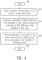
- Step 400 Start.
- Step 402 Write a plurality of data cells in a TDI block to at least one buffer.
- Step 404 Generate a plurality of DDR addresses of the plurality of data cells according to a plurality of TDI addresses of the plurality of data cells.
- Step 406 Write the plurality of data cells in the at least one buffer to a DDR storage device according to the plurality of DDR addresses.
- Step 408 End.
- the process 40 is used for illustrating the operations of the TDI 20. Detailed description and variations of the process 40 can be referred to the previous description, and is not narrated herein.
- Fig. 5 is a schematic diagram of a time de-interleaver (TDI) 50 according to the present invention.
- the TDI 50 may be utilized in the receiver RX of Fig. 1 , for handling data cells in a DDR storage device.
- the TDI 50 includes a DDR storage device 500, a cache 502, a DDR reading circuit 504 and a cache writing circuit 506.
- the DDR reading circuit 504 is coupled to the DDR storage device 500, and reads a first part of the data cells in the DDR storage device 500.
- the cache writing circuit 506 is coupled to the DDR reading circuit 504 and the cache 502, and writes (e.g., stores) the first part of the data cells in the DDR storage device 500 to the cache 502.
- the receiver RX may obtain the first part of the data cells form the cache 502 instead of the DDR storage device 500, and may process the first part of the data cells.
- the DDR reading circuit 504 reads a second part of the data cells in the DDR storage device 500, e.g., when the first part of the data cells in the cache 502 is not needed for the receiver RX.
- the cache writing circuit 506 writes (e.g., stores) the second part of the data cells in the DDR storage device 500 to the cache 502.
- the receiver RX may obtain the second part of the data cells form the cache 502, and may process the second part of the data cells.
- the DDR reading circuit 504 reads the first part of the data cells in the DDR storage device 500 by using a DDR R/W. In one example, after the receiver RX obtains (or processes) the first part of the data cells (e.g., the first part of the data cells in the cache 502 is no longer needed for the receiver RX), the DDR reading circuit 504 reads the second part of the data cells in the DDR storage device 500 by using the DDR R/W.
- the DDR reading circuit 504 reads a third part of the data cells in the DDR storage device 500 by using the DDR R/W.
- the first part of the data cells and the second part of the data cells are not overlapped in the DDR storage device 500.
- the second part of the data cells and the third part of the data cells are not overlapped in the DDR storage device 500.
- a capacity of the cache 502 is not smaller than the capacity of the DDR R/W. That is, the minimum capacity of the cache 502 is equal to the capacity of the DDR R/W.
- the following example is used for illustrating how the TDI 50 handles the data cells in the DDR storage device 500.
- a data cell with a size of 32 bits and the DDR R/W with a capacity of 256 bits are assumed. That is, the TDI 50 reads 8 data cells at a time by using the DDR R/W.
- the minimum capacity of the cache 502 is 256 bits.
- the DDR reading circuit 504 reads 8 data cells of the data cells in the DDR storage device 500 (e.g., the DDR storage device 302 with DDR addresses 128-135) by using the DDR R/W, and the cache writing circuit 506 writes the 8 data cells to the cache 502. That is, the receiver RX may obtain the 8 data cells from the cache 502, and may process the 8 data cells.
- the DDR reading circuit 504 reads other 8 data cells of the data cells in the DDR storage device 500 (e.g., the DDR storage device 302 with DDR addresses 136-143) by using the DDR R/W, and the cache writing circuit 506 writes the other 8 data cells to the cache 502.
- the DDR reading circuit 504 needs to read 2048 (i.e., 16 ⁇ 1024/8) times to read all the data cells in the DDR storage device 500.
- the DDR reading circuit 504 reads the data cells in the DDR storage device 500 according to an order of the cell numbers. For example, the DDR reading circuit 504 first reads a data cell with a cell number 0 (i.e., the data cell with a TDI address (1, 1) in the TDI block 300) by reading 8 data cells with TDI addresses (1, 1), (1, 2), ... , (1, 8).
- the data cell with the TDI address (1, 1) is useful for the receiver RX, while the other 7 data cells are useless. That is, the receiver RX uses only one cell read by the DDR reading circuit 504.
- the DDR reading circuit 504 reads a data cell with a cell number 1 (i.e., the data cell with a TDI address (2, 2) in the TDI block 300) by reading 8 data cells with TDI addresses (2,1), (2, 2), ..., (2, 8).
- the data cell with the TDI address (2, 2) is useful for the receiver RX, while the other 7 data cells are useless.
- the DDR reading circuit 504 needs to read 16384 (i.e., 16 ⁇ 1024) times to read all the data cells in the DDR storage device 500.
- the resource consumption e.g., the number of TDI reading
- Step 600 Start.
- Step 602 Read a first part of a plurality of data cells in a DDR storage device.
- Step 604 Write the first part of the plurality of data cells in the DDR storage device to a cache.
- Step 606 End.
- the process 60 is used for illustrating the operations of the TDI 50. Detailed description and variations of the process 60 can be referred to the previous description, and is not narrated herein.
- the TDI 20 including the at least one buffer 200, the DDR storage device 202, the buffer writing circuit 204, the control circuit 206 and the DDR writing circuit 208) and the TDI 50 (including the DDR storage device 500, the cache 502, the DDR reading circuit 504 and the cache writing circuit 506) are various.
- the circuits mentioned above may be integrated into one or more circuits.
- the TDI 20 and the TDI 50 may be realized by hardware (e.g., circuit), software, firmware (known as a combination of a hardware device, computer instructions and data that reside as read-only software on the hardware device), an electronic system or a combination of the devices mentioned above, but is not limited herein.
- the present invention provides a device for handling a TDI block.
- a TDI generates DDR addresses, and writes data cells in a TDI block to a DDR storage device according to the DDR addresses, to reduce the resource consumption. Thus, better efficiency is achieved.
Landscapes
- Engineering & Computer Science (AREA)
- Theoretical Computer Science (AREA)
- Physics & Mathematics (AREA)
- General Engineering & Computer Science (AREA)
- General Physics & Mathematics (AREA)
- Mobile Radio Communication Systems (AREA)
- Error Detection And Correction (AREA)
Claims (1)
- Zeit-Entschachtelungsvorrichtung, TDI, (20), welche umfasst:mindestens einen Puffer (200);eine Doppeldatenraten-, DDR, Speichervorrichtung (202);eine Pufferschreibschaltung (204), die mit dem mindestens einen Puffer (200) gekoppelt ist, zum Schreiben mehrerer Datenzellen in einem TDI-Block in den mindestens einen Puffer (200) (402);eine Steuerschaltung (206), die mit der Pufferschreibschaltung (204) gekoppelt ist, zum Erzeugen mehrerer DDR-Adressen der mehreren Datenzellen gemäß mehrerer TDI-Adressen der mehreren Datenzellen gemäß der folgenden Gleichung:
 wobei Nc eine Anzahl von Spalten des TDI-Blocks ist, (R,C) eine der mehreren von TDI-Adressen ist, Nb eine Anzahl des mindestens einen Puffers (200) ist und BUF ein Parameter ist, der sich auf ein Verhältnis einer Kapazität eines DDR-Lese-/Schreibvorgangs (R/W) und einer Größe von einer der mehreren Datenzellen bezieht; undeine DDR-Schreibschaltung (208), die mit der Steuerschaltung (206) und der DDR-Speichervorrichtung (202) gekoppelt ist, zum Schreiben der mehreren Datenzellen in dem mindestens einen Puffer (200) in die DDR-Speichervorrichtung (202) gemäß den mehreren DDR-Adressen (406), wenn der mindestens eine Puffer (200) voll ist.
Priority Applications (1)
| Application Number | Priority Date | Filing Date | Title |
|---|---|---|---|
| EP19158480.4A EP3699767B1 (de) | 2019-02-21 | 2019-02-21 | Vorrichtung und verfahren zur handhabung eines zeitentschachtelerblocks |
Applications Claiming Priority (1)
| Application Number | Priority Date | Filing Date | Title |
|---|---|---|---|
| EP19158480.4A EP3699767B1 (de) | 2019-02-21 | 2019-02-21 | Vorrichtung und verfahren zur handhabung eines zeitentschachtelerblocks |
Publications (2)
| Publication Number | Publication Date |
|---|---|
| EP3699767A1 EP3699767A1 (de) | 2020-08-26 |
| EP3699767B1 true EP3699767B1 (de) | 2025-02-19 |
Family
ID=65520112
Family Applications (1)
| Application Number | Title | Priority Date | Filing Date |
|---|---|---|---|
| EP19158480.4A Active EP3699767B1 (de) | 2019-02-21 | 2019-02-21 | Vorrichtung und verfahren zur handhabung eines zeitentschachtelerblocks |
Country Status (1)
| Country | Link |
|---|---|
| EP (1) | EP3699767B1 (de) |
Family Cites Families (6)
| Publication number | Priority date | Publication date | Assignee | Title |
|---|---|---|---|---|
| EP0856949B1 (de) * | 1997-01-31 | 2005-03-30 | Alcatel | Verfahren und Geräte zur Schachtelung/Entschachtelung von digitalen Daten und Kommunikationssystem |
| US7600163B2 (en) * | 2003-09-23 | 2009-10-06 | Realtek Semiconductor Corp. | Convolutional interleaver and deinterleaver |
| US7764595B2 (en) * | 2008-01-16 | 2010-07-27 | Newport Media, Inc. | Area and power efficient architectures of time deinterleaver for ISDB-T receivers |
| US7945746B2 (en) * | 2008-06-02 | 2011-05-17 | Newport Media, Inc. | Memory sharing of time and frequency de-interleaver for ISDB-T receivers |
| US8379671B2 (en) * | 2009-01-30 | 2013-02-19 | Freescale Semiconductor, Inc. | Techniques for extracting a control channel from a received signal in a wireless communication system |
| US8352834B2 (en) * | 2009-11-12 | 2013-01-08 | Broadlogic Network Technologies Inc. | High throughput interleaver / deinterleaver |
-
2019
- 2019-02-21 EP EP19158480.4A patent/EP3699767B1/de active Active
Also Published As
| Publication number | Publication date |
|---|---|
| EP3699767A1 (de) | 2020-08-26 |
Similar Documents
| Publication | Publication Date | Title |
|---|---|---|
| US8059737B2 (en) | OFDM receiver having memory capable of acting in a single-chip mode and a diversity mode | |
| EP3340507A1 (de) | Verfahren zur übertragung von daten, basisstation und endgeräteausrüstung | |
| US20100283912A1 (en) | Apparatus for Demodulating Digital Video and Associated Method | |
| US20100174769A1 (en) | In-Place Fast Fourier Transform Processor | |
| WO2018228601A1 (zh) | 一种数据处理方法及数据处理装置 | |
| JP2013504975A (ja) | ハイブリッド自動再送要求(harq)プロトコルのスループットを高める方法およびシステム | |
| WO2019091374A1 (zh) | 传输信息的方法和通信设备 | |
| US20200178234A1 (en) | Information Sending Method And Device | |
| US11457423B2 (en) | Radio communications | |
| WO2019042370A1 (zh) | 数据传输方法及装置 | |
| JPWO2011064837A1 (ja) | 受信機、受信方法及び受信制御プログラム | |
| WO2020063284A1 (zh) | 通信方法及装置 | |
| US10140209B2 (en) | Time de-interleaving circuit and time de-interleaving method for reducing a number of times of accessing memory | |
| CN102215097A (zh) | 一种管理混合自动重传请求缓存的方法及装置 | |
| CN108809582B (zh) | 一种数据传输的方法和装置 | |
| EP3699767A1 (de) | Vorrichtung und verfahren zur handhabung eines zeitentschachtelerblocks | |
| CN112152641B (zh) | 数据交织方法、装置及数据发送设备 | |
| US20190379515A1 (en) | Method and device for dividing short transmission time interval of special subframe | |
| US10164664B2 (en) | Time and cell de-interleaving circuit and method for performing time and cell de-interleaving | |
| WO2021077874A1 (zh) | 解交织方法及装置 | |
| WO2019047947A1 (zh) | 用于在无线通信系统中交织数据的方法和设备 | |
| CN113541707B (zh) | 一种滤波方法、通信装置、芯片及其模组设备 | |
| CN106571900B (zh) | 一种低延时的无线通信方法和装置 | |
| CN114415946B (zh) | 解速率匹配的方法及装置、终端设备、芯片及存储介质 | |
| US20160164636A1 (en) | Frequency deinterleaving and time deinterleaving circuit, method thereof and receiving circuit of digital television |
Legal Events
| Date | Code | Title | Description |
|---|---|---|---|
| PUAI | Public reference made under article 153(3) epc to a published international application that has entered the european phase |
Free format text: ORIGINAL CODE: 0009012 |
|
| STAA | Information on the status of an ep patent application or granted ep patent |
Free format text: STATUS: THE APPLICATION HAS BEEN PUBLISHED |
|
| AK | Designated contracting states |
Kind code of ref document: A1 Designated state(s): AL AT BE BG CH CY CZ DE DK EE ES FI FR GB GR HR HU IE IS IT LI LT LU LV MC MK MT NL NO PL PT RO RS SE SI SK SM TR |
|
| AX | Request for extension of the european patent |
Extension state: BA ME |
|
| STAA | Information on the status of an ep patent application or granted ep patent |
Free format text: STATUS: REQUEST FOR EXAMINATION WAS MADE |
|
| 17P | Request for examination filed |
Effective date: 20210108 |
|
| RBV | Designated contracting states (corrected) |
Designated state(s): AL AT BE BG CH CY CZ DE DK EE ES FI FR GB GR HR HU IE IS IT LI LT LU LV MC MK MT NL NO PL PT RO RS SE SI SK SM TR |
|
| STAA | Information on the status of an ep patent application or granted ep patent |
Free format text: STATUS: EXAMINATION IS IN PROGRESS |
|
| 17Q | First examination report despatched |
Effective date: 20220512 |
|
| GRAP | Despatch of communication of intention to grant a patent |
Free format text: ORIGINAL CODE: EPIDOSNIGR1 |
|
| STAA | Information on the status of an ep patent application or granted ep patent |
Free format text: STATUS: GRANT OF PATENT IS INTENDED |
|
| INTG | Intention to grant announced |
Effective date: 20241009 |
|
| P01 | Opt-out of the competence of the unified patent court (upc) registered |
Free format text: CASE NUMBER: APP_56921/2024 Effective date: 20241018 |
|
| GRAS | Grant fee paid |
Free format text: ORIGINAL CODE: EPIDOSNIGR3 |
|
| GRAA | (expected) grant |
Free format text: ORIGINAL CODE: 0009210 |
|
| STAA | Information on the status of an ep patent application or granted ep patent |
Free format text: STATUS: THE PATENT HAS BEEN GRANTED |
|
| AK | Designated contracting states |
Kind code of ref document: B1 Designated state(s): AL AT BE BG CH CY CZ DE DK EE ES FI FR GB GR HR HU IE IS IT LI LT LU LV MC MK MT NL NO PL PT RO RS SE SI SK SM TR |
|
| REG | Reference to a national code |
Ref country code: GB Ref legal event code: FG4D |
|
| REG | Reference to a national code |
Ref country code: CH Ref legal event code: EP |
|
| REG | Reference to a national code |
Ref country code: DE Ref legal event code: R096 Ref document number: 602019066038 Country of ref document: DE |
|
| REG | Reference to a national code |
Ref country code: IE Ref legal event code: FG4D |
|
| REG | Reference to a national code |
Ref country code: NL Ref legal event code: MP Effective date: 20250219 |
|
| PG25 | Lapsed in a contracting state [announced via postgrant information from national office to epo] |
Ref country code: RS Free format text: LAPSE BECAUSE OF FAILURE TO SUBMIT A TRANSLATION OF THE DESCRIPTION OR TO PAY THE FEE WITHIN THE PRESCRIBED TIME-LIMIT Effective date: 20250519 |
|
| PG25 | Lapsed in a contracting state [announced via postgrant information from national office to epo] |
Ref country code: FI Free format text: LAPSE BECAUSE OF FAILURE TO SUBMIT A TRANSLATION OF THE DESCRIPTION OR TO PAY THE FEE WITHIN THE PRESCRIBED TIME-LIMIT Effective date: 20250219 |
|
| PG25 | Lapsed in a contracting state [announced via postgrant information from national office to epo] |
Ref country code: PL Free format text: LAPSE BECAUSE OF FAILURE TO SUBMIT A TRANSLATION OF THE DESCRIPTION OR TO PAY THE FEE WITHIN THE PRESCRIBED TIME-LIMIT Effective date: 20250219 |
|
| PG25 | Lapsed in a contracting state [announced via postgrant information from national office to epo] |
Ref country code: ES Free format text: LAPSE BECAUSE OF FAILURE TO SUBMIT A TRANSLATION OF THE DESCRIPTION OR TO PAY THE FEE WITHIN THE PRESCRIBED TIME-LIMIT Effective date: 20250219 |
|
| REG | Reference to a national code |
Ref country code: LT Ref legal event code: MG9D |
|
| PG25 | Lapsed in a contracting state [announced via postgrant information from national office to epo] |
Ref country code: IS Free format text: LAPSE BECAUSE OF FAILURE TO SUBMIT A TRANSLATION OF THE DESCRIPTION OR TO PAY THE FEE WITHIN THE PRESCRIBED TIME-LIMIT Effective date: 20250619 Ref country code: NO Free format text: LAPSE BECAUSE OF FAILURE TO SUBMIT A TRANSLATION OF THE DESCRIPTION OR TO PAY THE FEE WITHIN THE PRESCRIBED TIME-LIMIT Effective date: 20250519 |
|
| PG25 | Lapsed in a contracting state [announced via postgrant information from national office to epo] |
Ref country code: NL Free format text: LAPSE BECAUSE OF FAILURE TO SUBMIT A TRANSLATION OF THE DESCRIPTION OR TO PAY THE FEE WITHIN THE PRESCRIBED TIME-LIMIT Effective date: 20250219 |
|
| PG25 | Lapsed in a contracting state [announced via postgrant information from national office to epo] |
Ref country code: HR Free format text: LAPSE BECAUSE OF FAILURE TO SUBMIT A TRANSLATION OF THE DESCRIPTION OR TO PAY THE FEE WITHIN THE PRESCRIBED TIME-LIMIT Effective date: 20250219 |
|
| PG25 | Lapsed in a contracting state [announced via postgrant information from national office to epo] |
Ref country code: LV Free format text: LAPSE BECAUSE OF FAILURE TO SUBMIT A TRANSLATION OF THE DESCRIPTION OR TO PAY THE FEE WITHIN THE PRESCRIBED TIME-LIMIT Effective date: 20250219 Ref country code: PT Free format text: LAPSE BECAUSE OF FAILURE TO SUBMIT A TRANSLATION OF THE DESCRIPTION OR TO PAY THE FEE WITHIN THE PRESCRIBED TIME-LIMIT Effective date: 20250620 |
|
| PG25 | Lapsed in a contracting state [announced via postgrant information from national office to epo] |
Ref country code: BG Free format text: LAPSE BECAUSE OF FAILURE TO SUBMIT A TRANSLATION OF THE DESCRIPTION OR TO PAY THE FEE WITHIN THE PRESCRIBED TIME-LIMIT Effective date: 20250219 Ref country code: GR Free format text: LAPSE BECAUSE OF FAILURE TO SUBMIT A TRANSLATION OF THE DESCRIPTION OR TO PAY THE FEE WITHIN THE PRESCRIBED TIME-LIMIT Effective date: 20250520 |
|
| REG | Reference to a national code |
Ref country code: AT Ref legal event code: MK05 Ref document number: 1768958 Country of ref document: AT Kind code of ref document: T Effective date: 20250219 |
|
| PG25 | Lapsed in a contracting state [announced via postgrant information from national office to epo] |
Ref country code: SE Free format text: LAPSE BECAUSE OF FAILURE TO SUBMIT A TRANSLATION OF THE DESCRIPTION OR TO PAY THE FEE WITHIN THE PRESCRIBED TIME-LIMIT Effective date: 20250219 |
|
| REG | Reference to a national code |
Ref country code: CH Ref legal event code: PL |
|
| PG25 | Lapsed in a contracting state [announced via postgrant information from national office to epo] |
Ref country code: SM Free format text: LAPSE BECAUSE OF FAILURE TO SUBMIT A TRANSLATION OF THE DESCRIPTION OR TO PAY THE FEE WITHIN THE PRESCRIBED TIME-LIMIT Effective date: 20250219 |
|
| PG25 | Lapsed in a contracting state [announced via postgrant information from national office to epo] |
Ref country code: DK Free format text: LAPSE BECAUSE OF FAILURE TO SUBMIT A TRANSLATION OF THE DESCRIPTION OR TO PAY THE FEE WITHIN THE PRESCRIBED TIME-LIMIT Effective date: 20250219 |
|
| PG25 | Lapsed in a contracting state [announced via postgrant information from national office to epo] |
Ref country code: LU Free format text: LAPSE BECAUSE OF NON-PAYMENT OF DUE FEES Effective date: 20250221 Ref country code: IT Free format text: LAPSE BECAUSE OF FAILURE TO SUBMIT A TRANSLATION OF THE DESCRIPTION OR TO PAY THE FEE WITHIN THE PRESCRIBED TIME-LIMIT Effective date: 20250219 |
|
| PG25 | Lapsed in a contracting state [announced via postgrant information from national office to epo] |
Ref country code: AT Free format text: LAPSE BECAUSE OF FAILURE TO SUBMIT A TRANSLATION OF THE DESCRIPTION OR TO PAY THE FEE WITHIN THE PRESCRIBED TIME-LIMIT Effective date: 20250219 |
|
| PG25 | Lapsed in a contracting state [announced via postgrant information from national office to epo] |
Ref country code: CH Free format text: LAPSE BECAUSE OF NON-PAYMENT OF DUE FEES Effective date: 20250228 |
|
| PG25 | Lapsed in a contracting state [announced via postgrant information from national office to epo] |
Ref country code: EE Free format text: LAPSE BECAUSE OF FAILURE TO SUBMIT A TRANSLATION OF THE DESCRIPTION OR TO PAY THE FEE WITHIN THE PRESCRIBED TIME-LIMIT Effective date: 20250219 Ref country code: CZ Free format text: LAPSE BECAUSE OF FAILURE TO SUBMIT A TRANSLATION OF THE DESCRIPTION OR TO PAY THE FEE WITHIN THE PRESCRIBED TIME-LIMIT Effective date: 20250219 |
|
| PG25 | Lapsed in a contracting state [announced via postgrant information from national office to epo] |
Ref country code: RO Free format text: LAPSE BECAUSE OF FAILURE TO SUBMIT A TRANSLATION OF THE DESCRIPTION OR TO PAY THE FEE WITHIN THE PRESCRIBED TIME-LIMIT Effective date: 20250219 |
|
| PG25 | Lapsed in a contracting state [announced via postgrant information from national office to epo] |
Ref country code: SK Free format text: LAPSE BECAUSE OF FAILURE TO SUBMIT A TRANSLATION OF THE DESCRIPTION OR TO PAY THE FEE WITHIN THE PRESCRIBED TIME-LIMIT Effective date: 20250219 |
|
| REG | Reference to a national code |
Ref country code: DE Ref legal event code: R097 Ref document number: 602019066038 Country of ref document: DE |
|
| REG | Reference to a national code |
Ref country code: BE Ref legal event code: MM Effective date: 20250228 |
|
| PG25 | Lapsed in a contracting state [announced via postgrant information from national office to epo] |
Ref country code: MC Free format text: LAPSE BECAUSE OF FAILURE TO SUBMIT A TRANSLATION OF THE DESCRIPTION OR TO PAY THE FEE WITHIN THE PRESCRIBED TIME-LIMIT Effective date: 20250219 |
|
| PLBE | No opposition filed within time limit |
Free format text: ORIGINAL CODE: 0009261 |
|
| STAA | Information on the status of an ep patent application or granted ep patent |
Free format text: STATUS: NO OPPOSITION FILED WITHIN TIME LIMIT |
|
| PG25 | Lapsed in a contracting state [announced via postgrant information from national office to epo] |
Ref country code: BE Free format text: LAPSE BECAUSE OF NON-PAYMENT OF DUE FEES Effective date: 20250228 |
|
| PG25 | Lapsed in a contracting state [announced via postgrant information from national office to epo] |
Ref country code: IE Free format text: LAPSE BECAUSE OF NON-PAYMENT OF DUE FEES Effective date: 20250221 |
|
| 26N | No opposition filed |
Effective date: 20251120 |
|
| PGFP | Annual fee paid to national office [announced via postgrant information from national office to epo] |
Ref country code: GB Payment date: 20260106 Year of fee payment: 8 |
|
| PGFP | Annual fee paid to national office [announced via postgrant information from national office to epo] |
Ref country code: DE Payment date: 20260109 Year of fee payment: 8 |
|
| PGFP | Annual fee paid to national office [announced via postgrant information from national office to epo] |
Ref country code: FR Payment date: 20260106 Year of fee payment: 8 |