EP0856164B1 - Bistable nematic liquid crystal device - Google Patents
Bistable nematic liquid crystal device Download PDFInfo
- Publication number
- EP0856164B1 EP0856164B1 EP96932739A EP96932739A EP0856164B1 EP 0856164 B1 EP0856164 B1 EP 0856164B1 EP 96932739 A EP96932739 A EP 96932739A EP 96932739 A EP96932739 A EP 96932739A EP 0856164 B1 EP0856164 B1 EP 0856164B1
- Authority
- EP
- European Patent Office
- Prior art keywords
- liquid crystal
- cell
- alignment
- grating
- bistable
- Prior art date
- Legal status (The legal status is an assumption and is not a legal conclusion. Google has not performed a legal analysis and makes no representation as to the accuracy of the status listed.)
- Expired - Lifetime
Links
- 239000004988 Nematic liquid crystal Substances 0.000 title claims abstract description 13
- 239000000463 material Substances 0.000 claims abstract description 38
- 210000002421 cell wall Anatomy 0.000 claims abstract description 31
- 239000011159 matrix material Substances 0.000 claims abstract description 8
- 230000008878 coupling Effects 0.000 claims abstract description 7
- 238000010168 coupling process Methods 0.000 claims abstract description 7
- 238000005859 coupling reaction Methods 0.000 claims abstract description 7
- 239000004973 liquid crystal related substance Substances 0.000 claims description 37
- 239000004094 surface-active agent Substances 0.000 claims description 5
- 230000003098 cholesteric effect Effects 0.000 claims description 3
- 239000002019 doping agent Substances 0.000 claims description 2
- 210000004027 cell Anatomy 0.000 abstract description 56
- 238000000034 method Methods 0.000 abstract description 9
- 238000004049 embossing Methods 0.000 abstract description 3
- 239000004033 plastic Substances 0.000 abstract description 3
- 229920003023 plastic Polymers 0.000 abstract description 3
- 230000008569 process Effects 0.000 abstract description 2
- 238000004381 surface treatment Methods 0.000 abstract description 2
- 230000003287 optical effect Effects 0.000 description 8
- 230000005540 biological transmission Effects 0.000 description 7
- 229920002120 photoresistant polymer Polymers 0.000 description 7
- 230000004044 response Effects 0.000 description 7
- 238000004630 atomic force microscopy Methods 0.000 description 5
- 239000011521 glass Substances 0.000 description 5
- CSCPPACGZOOCGX-UHFFFAOYSA-N Acetone Chemical compound CC(C)=O CSCPPACGZOOCGX-UHFFFAOYSA-N 0.000 description 4
- KFZMGEQAYNKOFK-UHFFFAOYSA-N Isopropanol Chemical compound CC(C)O KFZMGEQAYNKOFK-UHFFFAOYSA-N 0.000 description 4
- 238000004458 analytical method Methods 0.000 description 4
- 238000004873 anchoring Methods 0.000 description 4
- 230000008859 change Effects 0.000 description 4
- 238000000576 coating method Methods 0.000 description 4
- 238000001704 evaporation Methods 0.000 description 4
- 230000008020 evaporation Effects 0.000 description 4
- 150000002500 ions Chemical class 0.000 description 4
- VYZAMTAEIAYCRO-UHFFFAOYSA-N Chromium Chemical compound [Cr] VYZAMTAEIAYCRO-UHFFFAOYSA-N 0.000 description 3
- 230000004888 barrier function Effects 0.000 description 3
- 230000000694 effects Effects 0.000 description 3
- 230000005684 electric field Effects 0.000 description 3
- 239000000203 mixture Substances 0.000 description 3
- IIZPXYDJLKNOIY-JXPKJXOSSA-N 1-palmitoyl-2-arachidonoyl-sn-glycero-3-phosphocholine Chemical compound CCCCCCCCCCCCCCCC(=O)OC[C@H](COP([O-])(=O)OCC[N+](C)(C)C)OC(=O)CCC\C=C/C\C=C/C\C=C/C\C=C/CCCCC IIZPXYDJLKNOIY-JXPKJXOSSA-N 0.000 description 2
- 239000004642 Polyimide Substances 0.000 description 2
- 239000004990 Smectic liquid crystal Substances 0.000 description 2
- 239000011248 coating agent Substances 0.000 description 2
- 238000001816 cooling Methods 0.000 description 2
- 239000008367 deionised water Substances 0.000 description 2
- 238000009826 distribution Methods 0.000 description 2
- 239000005262 ferroelectric liquid crystals (FLCs) Substances 0.000 description 2
- 239000000787 lecithin Substances 0.000 description 2
- 229940067606 lecithin Drugs 0.000 description 2
- 235000010445 lecithin Nutrition 0.000 description 2
- 238000004519 manufacturing process Methods 0.000 description 2
- QSHDDOUJBYECFT-UHFFFAOYSA-N mercury Chemical compound [Hg] QSHDDOUJBYECFT-UHFFFAOYSA-N 0.000 description 2
- 229910052753 mercury Inorganic materials 0.000 description 2
- 229920001721 polyimide Polymers 0.000 description 2
- 229920000642 polymer Polymers 0.000 description 2
- 230000005855 radiation Effects 0.000 description 2
- 238000000926 separation method Methods 0.000 description 2
- XOLBLPGZBRYERU-UHFFFAOYSA-N tin dioxide Chemical compound O=[Sn]=O XOLBLPGZBRYERU-UHFFFAOYSA-N 0.000 description 2
- 230000001052 transient effect Effects 0.000 description 2
- NWCHELUCVWSRRS-SECBINFHSA-N (2r)-2-hydroxy-2-phenylpropanoic acid Chemical compound OC(=O)[C@@](O)(C)C1=CC=CC=C1 NWCHELUCVWSRRS-SECBINFHSA-N 0.000 description 1
- CPELXLSAUQHCOX-UHFFFAOYSA-M Bromide Chemical compound [Br-] CPELXLSAUQHCOX-UHFFFAOYSA-M 0.000 description 1
- 239000004986 Cholesteric liquid crystals (ChLC) Substances 0.000 description 1
- OWYWGLHRNBIFJP-UHFFFAOYSA-N Ipazine Chemical compound CCN(CC)C1=NC(Cl)=NC(NC(C)C)=N1 OWYWGLHRNBIFJP-UHFFFAOYSA-N 0.000 description 1
- 239000004743 Polypropylene Substances 0.000 description 1
- 239000011324 bead Substances 0.000 description 1
- 230000008901 benefit Effects 0.000 description 1
- 125000001797 benzyl group Chemical group [H]C1=C([H])C([H])=C(C([H])=C1[H])C([H])([H])* 0.000 description 1
- 230000015572 biosynthetic process Effects 0.000 description 1
- 239000013590 bulk material Substances 0.000 description 1
- 238000010276 construction Methods 0.000 description 1
- 210000002858 crystal cell Anatomy 0.000 description 1
- 230000007423 decrease Effects 0.000 description 1
- 230000007547 defect Effects 0.000 description 1
- 230000001419 dependent effect Effects 0.000 description 1
- 230000008021 deposition Effects 0.000 description 1
- 238000005516 engineering process Methods 0.000 description 1
- 238000002474 experimental method Methods 0.000 description 1
- AMGQUBHHOARCQH-UHFFFAOYSA-N indium;oxotin Chemical compound [In].[Sn]=O AMGQUBHHOARCQH-UHFFFAOYSA-N 0.000 description 1
- 230000001939 inductive effect Effects 0.000 description 1
- 230000001151 other effect Effects 0.000 description 1
- 229920000098 polyolefin Polymers 0.000 description 1
- -1 polypropylene Polymers 0.000 description 1
- 229920001155 polypropylene Polymers 0.000 description 1
- 230000002040 relaxant effect Effects 0.000 description 1
- 230000035939 shock Effects 0.000 description 1
- 239000007787 solid Substances 0.000 description 1
- 125000006850 spacer group Chemical group 0.000 description 1
- 239000000758 substrate Substances 0.000 description 1
- 239000010409 thin film Substances 0.000 description 1
Images


Classifications
-
- G—PHYSICS
- G02—OPTICS
- G02F—OPTICAL DEVICES OR ARRANGEMENTS FOR THE CONTROL OF LIGHT BY MODIFICATION OF THE OPTICAL PROPERTIES OF THE MEDIA OF THE ELEMENTS INVOLVED THEREIN; NON-LINEAR OPTICS; FREQUENCY-CHANGING OF LIGHT; OPTICAL LOGIC ELEMENTS; OPTICAL ANALOGUE/DIGITAL CONVERTERS
- G02F1/00—Devices or arrangements for the control of the intensity, colour, phase, polarisation or direction of light arriving from an independent light source, e.g. switching, gating or modulating; Non-linear optics
- G02F1/01—Devices or arrangements for the control of the intensity, colour, phase, polarisation or direction of light arriving from an independent light source, e.g. switching, gating or modulating; Non-linear optics for the control of the intensity, phase, polarisation or colour
- G02F1/13—Devices or arrangements for the control of the intensity, colour, phase, polarisation or direction of light arriving from an independent light source, e.g. switching, gating or modulating; Non-linear optics for the control of the intensity, phase, polarisation or colour based on liquid crystals, e.g. single liquid crystal display cells
- G02F1/133—Constructional arrangements; Operation of liquid crystal cells; Circuit arrangements
- G02F1/1333—Constructional arrangements; Manufacturing methods
- G02F1/1337—Surface-induced orientation of the liquid crystal molecules, e.g. by alignment layers
- G02F1/13378—Surface-induced orientation of the liquid crystal molecules, e.g. by alignment layers by treatment of the surface, e.g. embossing, rubbing or light irradiation
-
- G—PHYSICS
- G02—OPTICS
- G02F—OPTICAL DEVICES OR ARRANGEMENTS FOR THE CONTROL OF LIGHT BY MODIFICATION OF THE OPTICAL PROPERTIES OF THE MEDIA OF THE ELEMENTS INVOLVED THEREIN; NON-LINEAR OPTICS; FREQUENCY-CHANGING OF LIGHT; OPTICAL LOGIC ELEMENTS; OPTICAL ANALOGUE/DIGITAL CONVERTERS
- G02F1/00—Devices or arrangements for the control of the intensity, colour, phase, polarisation or direction of light arriving from an independent light source, e.g. switching, gating or modulating; Non-linear optics
- G02F1/01—Devices or arrangements for the control of the intensity, colour, phase, polarisation or direction of light arriving from an independent light source, e.g. switching, gating or modulating; Non-linear optics for the control of the intensity, phase, polarisation or colour
- G02F1/13—Devices or arrangements for the control of the intensity, colour, phase, polarisation or direction of light arriving from an independent light source, e.g. switching, gating or modulating; Non-linear optics for the control of the intensity, phase, polarisation or colour based on liquid crystals, e.g. single liquid crystal display cells
- G02F1/133—Constructional arrangements; Operation of liquid crystal cells; Circuit arrangements
- G02F1/1333—Constructional arrangements; Manufacturing methods
- G02F1/1337—Surface-induced orientation of the liquid crystal molecules, e.g. by alignment layers
-
- G—PHYSICS
- G02—OPTICS
- G02F—OPTICAL DEVICES OR ARRANGEMENTS FOR THE CONTROL OF LIGHT BY MODIFICATION OF THE OPTICAL PROPERTIES OF THE MEDIA OF THE ELEMENTS INVOLVED THEREIN; NON-LINEAR OPTICS; FREQUENCY-CHANGING OF LIGHT; OPTICAL LOGIC ELEMENTS; OPTICAL ANALOGUE/DIGITAL CONVERTERS
- G02F1/00—Devices or arrangements for the control of the intensity, colour, phase, polarisation or direction of light arriving from an independent light source, e.g. switching, gating or modulating; Non-linear optics
- G02F1/01—Devices or arrangements for the control of the intensity, colour, phase, polarisation or direction of light arriving from an independent light source, e.g. switching, gating or modulating; Non-linear optics for the control of the intensity, phase, polarisation or colour
- G02F1/13—Devices or arrangements for the control of the intensity, colour, phase, polarisation or direction of light arriving from an independent light source, e.g. switching, gating or modulating; Non-linear optics for the control of the intensity, phase, polarisation or colour based on liquid crystals, e.g. single liquid crystal display cells
- G02F1/137—Devices or arrangements for the control of the intensity, colour, phase, polarisation or direction of light arriving from an independent light source, e.g. switching, gating or modulating; Non-linear optics for the control of the intensity, phase, polarisation or colour based on liquid crystals, e.g. single liquid crystal display cells characterised by the electro-optical or magneto-optical effect, e.g. field-induced phase transition, orientation effect, guest-host interaction or dynamic scattering
- G02F1/139—Devices or arrangements for the control of the intensity, colour, phase, polarisation or direction of light arriving from an independent light source, e.g. switching, gating or modulating; Non-linear optics for the control of the intensity, phase, polarisation or colour based on liquid crystals, e.g. single liquid crystal display cells characterised by the electro-optical or magneto-optical effect, e.g. field-induced phase transition, orientation effect, guest-host interaction or dynamic scattering based on orientation effects in which the liquid crystal remains transparent
- G02F1/1391—Bistable or multi-stable liquid crystal cells
-
- G—PHYSICS
- G02—OPTICS
- G02F—OPTICAL DEVICES OR ARRANGEMENTS FOR THE CONTROL OF LIGHT BY MODIFICATION OF THE OPTICAL PROPERTIES OF THE MEDIA OF THE ELEMENTS INVOLVED THEREIN; NON-LINEAR OPTICS; FREQUENCY-CHANGING OF LIGHT; OPTICAL LOGIC ELEMENTS; OPTICAL ANALOGUE/DIGITAL CONVERTERS
- G02F1/00—Devices or arrangements for the control of the intensity, colour, phase, polarisation or direction of light arriving from an independent light source, e.g. switching, gating or modulating; Non-linear optics
- G02F1/01—Devices or arrangements for the control of the intensity, colour, phase, polarisation or direction of light arriving from an independent light source, e.g. switching, gating or modulating; Non-linear optics for the control of the intensity, phase, polarisation or colour
- G02F1/13—Devices or arrangements for the control of the intensity, colour, phase, polarisation or direction of light arriving from an independent light source, e.g. switching, gating or modulating; Non-linear optics for the control of the intensity, phase, polarisation or colour based on liquid crystals, e.g. single liquid crystal display cells
- G02F1/133—Constructional arrangements; Operation of liquid crystal cells; Circuit arrangements
- G02F1/1333—Constructional arrangements; Manufacturing methods
- G02F1/1337—Surface-induced orientation of the liquid crystal molecules, e.g. by alignment layers
- G02F1/133765—Surface-induced orientation of the liquid crystal molecules, e.g. by alignment layers without a surface treatment
-
- G—PHYSICS
- G02—OPTICS
- G02F—OPTICAL DEVICES OR ARRANGEMENTS FOR THE CONTROL OF LIGHT BY MODIFICATION OF THE OPTICAL PROPERTIES OF THE MEDIA OF THE ELEMENTS INVOLVED THEREIN; NON-LINEAR OPTICS; FREQUENCY-CHANGING OF LIGHT; OPTICAL LOGIC ELEMENTS; OPTICAL ANALOGUE/DIGITAL CONVERTERS
- G02F1/00—Devices or arrangements for the control of the intensity, colour, phase, polarisation or direction of light arriving from an independent light source, e.g. switching, gating or modulating; Non-linear optics
- G02F1/01—Devices or arrangements for the control of the intensity, colour, phase, polarisation or direction of light arriving from an independent light source, e.g. switching, gating or modulating; Non-linear optics for the control of the intensity, phase, polarisation or colour
- G02F1/13—Devices or arrangements for the control of the intensity, colour, phase, polarisation or direction of light arriving from an independent light source, e.g. switching, gating or modulating; Non-linear optics for the control of the intensity, phase, polarisation or colour based on liquid crystals, e.g. single liquid crystal display cells
- G02F1/137—Devices or arrangements for the control of the intensity, colour, phase, polarisation or direction of light arriving from an independent light source, e.g. switching, gating or modulating; Non-linear optics for the control of the intensity, phase, polarisation or colour based on liquid crystals, e.g. single liquid crystal display cells characterised by the electro-optical or magneto-optical effect, e.g. field-induced phase transition, orientation effect, guest-host interaction or dynamic scattering
- G02F1/139—Devices or arrangements for the control of the intensity, colour, phase, polarisation or direction of light arriving from an independent light source, e.g. switching, gating or modulating; Non-linear optics for the control of the intensity, phase, polarisation or colour based on liquid crystals, e.g. single liquid crystal display cells characterised by the electro-optical or magneto-optical effect, e.g. field-induced phase transition, orientation effect, guest-host interaction or dynamic scattering based on orientation effects in which the liquid crystal remains transparent
- G02F1/1392—Devices or arrangements for the control of the intensity, colour, phase, polarisation or direction of light arriving from an independent light source, e.g. switching, gating or modulating; Non-linear optics for the control of the intensity, phase, polarisation or colour based on liquid crystals, e.g. single liquid crystal display cells characterised by the electro-optical or magneto-optical effect, e.g. field-induced phase transition, orientation effect, guest-host interaction or dynamic scattering based on orientation effects in which the liquid crystal remains transparent using a field-induced sign-reversal of the dielectric anisotropy
-
- G—PHYSICS
- G02—OPTICS
- G02F—OPTICAL DEVICES OR ARRANGEMENTS FOR THE CONTROL OF LIGHT BY MODIFICATION OF THE OPTICAL PROPERTIES OF THE MEDIA OF THE ELEMENTS INVOLVED THEREIN; NON-LINEAR OPTICS; FREQUENCY-CHANGING OF LIGHT; OPTICAL LOGIC ELEMENTS; OPTICAL ANALOGUE/DIGITAL CONVERTERS
- G02F1/00—Devices or arrangements for the control of the intensity, colour, phase, polarisation or direction of light arriving from an independent light source, e.g. switching, gating or modulating; Non-linear optics
- G02F1/01—Devices or arrangements for the control of the intensity, colour, phase, polarisation or direction of light arriving from an independent light source, e.g. switching, gating or modulating; Non-linear optics for the control of the intensity, phase, polarisation or colour
- G02F1/13—Devices or arrangements for the control of the intensity, colour, phase, polarisation or direction of light arriving from an independent light source, e.g. switching, gating or modulating; Non-linear optics for the control of the intensity, phase, polarisation or colour based on liquid crystals, e.g. single liquid crystal display cells
- G02F1/137—Devices or arrangements for the control of the intensity, colour, phase, polarisation or direction of light arriving from an independent light source, e.g. switching, gating or modulating; Non-linear optics for the control of the intensity, phase, polarisation or colour based on liquid crystals, e.g. single liquid crystal display cells characterised by the electro-optical or magneto-optical effect, e.g. field-induced phase transition, orientation effect, guest-host interaction or dynamic scattering
- G02F1/139—Devices or arrangements for the control of the intensity, colour, phase, polarisation or direction of light arriving from an independent light source, e.g. switching, gating or modulating; Non-linear optics for the control of the intensity, phase, polarisation or colour based on liquid crystals, e.g. single liquid crystal display cells characterised by the electro-optical or magneto-optical effect, e.g. field-induced phase transition, orientation effect, guest-host interaction or dynamic scattering based on orientation effects in which the liquid crystal remains transparent
- G02F1/1396—Devices or arrangements for the control of the intensity, colour, phase, polarisation or direction of light arriving from an independent light source, e.g. switching, gating or modulating; Non-linear optics for the control of the intensity, phase, polarisation or colour based on liquid crystals, e.g. single liquid crystal display cells characterised by the electro-optical or magneto-optical effect, e.g. field-induced phase transition, orientation effect, guest-host interaction or dynamic scattering based on orientation effects in which the liquid crystal remains transparent the liquid crystal being selectively controlled between a twisted state and a non-twisted state, e.g. TN-LC cell
Definitions
- This invention relates to bistable nematic liquid crystal devices.
- Liquid crystal devices typically comprise a thin layer of a liquid crystal material contained between cell walls. Optically transparent electrode structures on the walls allow an electric field to be applied across the layer causing a re-ordering of the liquid crystal molecules.
- liquid crystal material there are three known types of liquid crystal material, nematic, cholesteric, and smectic each having a different molecular ordering.
- the present invention concerns devices using nematic materials.
- the electrodes In order to provide displays with a large number of addressable elements it is common to make the electrodes as a series of row electrode on one wall and a series of column electrodes on the other cell wall. These form e.g. an x, y matrix of addressable elements or pixels and, for twisted nematic types of devices, are commonly addressed using rms. addressing methods.
- Twisted nematic and phase change type of liquid crystal devices are switched to an ON state by application of a suitable voltage, and allowed to switch to an OFF state when the applied voltage falls below a lower voltage level, i.e. these devices are monostable.
- a suitable voltage 90° or 270° degree twist as in US-4,596,446
- the number of elements that can be rms. addressed is limited by the steepness of a device transmission vs voltage curve as details by Alt and Pleschko in IEEE Trans ED vol ED 21 1974 pages 146-155.
- One way of improving the number of pixels is to incorporate thin film transistors adjacent each pixel; such displays are termed active matrix displays.
- An advantage of nematic type of devices is the relatively low voltage requirements. They are also mechanically stable and have wide temperature operating ranges. This allows construction of small and portable battery powered displays.
- Ferroelectric liquid crystal displays can be made into bistable device with the use of smectic liquid crystal materials and suitable cell wall surface alignment treatment.
- Such a device is a surface stabilised ferroelectric liquid crystal device (SSFELCDs) as described by:- L J Yu, H Lee, C S Bak and M M Labes, Phys Rev Lett 36, 7, 388 (1976); R B Meyer, Mol Cryst Liq Cryst. 40, 33 (1977); N A Clark and S T Lagerwall, Appl Phys Lett, 36, 11, 899 (1980).
- SSFELCDs surface stabilised ferroelectric liquid crystal device
- One disadvantage of ferroelectric devices is the relatively large voltage needed to switch the material. This high voltage makes small portable, battery powered displays expensive. Also these displays suffer from other problems such as lack of, shock resistance, limited temperature range and also electrically induced defects such as needles.
- bistable surface anchoring can be achieved using nematics then a display can be made which has the merits of both the above mentioned technologies but none of the problems.
- a device is described with the following characteristics:
- the cell is made using two surfaces which have SiO coatings of appropriate thickness and evaporation angle to allow two stable states to exist on each surface. Furthermore the two states on a surface are designed to differ in azimuthal angle by 45° and the surfaces are oriented such that each of the two resulting domains are untwisted.
- the surfaces are also oriented in such a way that the pretilted state on one surface lines up with the untilted state on the other surface and vice versa. Hence when filled with 5CB, the two states are seen as shown in Figures 7B and 7C.
- Patent US 4,333,708 describes a multistable liquid crystal device in which cell walls are profiled to provide an array of singular points. Such substrate configurations provide multistable configurations of the director alignments because disclination must be moved to switch between stable configurations. Switching is achieved by application of electric fields.
- bistable nematic device is described in GB.2,286,467-A.
- This uses accurately formed bigratings on at least one cell wall.
- the bigrating permits liquid crystal molecules to adopt two different angular aligned directions when suitable electrical signals are applied to cell electrodes, e.g. dc coupling to flexoelectric polarisation as described in Patent Application No. WO.92/00546. Since in the two splayed state the director is quite close to being in the plane of the layer, the coupling between director and flexoelectric component can be small, which may hinder switching in some circumstances.
- the above disadvantages are overcome by a surface treatment to at least one cell wall that permits nematic liquid crystal molecules to adopt either of two pretilt angles in the same azimuthal plane.
- the cell can be electrically switched between these two states to allow information display which can persist after the removal of power.
- a bistable nematic liquid crystal device comprises:
- the grating may have a symmetric or an asymmetric groove profile.
- the grating may have an asymmetric groove profile which will induce a pretilt of less than 90°, e.g. 50° to 90°.
- the gratings may be applied to both cell walls and may be the same or different shape on each wall. Furthermore the grating profile may vary within each pixel area, and or in the inter pixel gaps between electrodes. One or both cell walls may be coated with a surfactant such as lethecin.
- the liquid crystal material may be non twisted in one or both stable molecular configurations.
- the cell walls may be formed of a relatively thick non flexible material such as a glass, or one or both cells walls may be formed of a flexible material such as a thin layer of glass or a plastic material flexible e.g. polyolefin or polypropylene.
- a plastic cell wall may be embossed on its inner surface to provide a grating. Additionally, the embossing may provide small pillars (e.g. of 1-3 ⁇ m height and 5-50 ⁇ m or more width) for assisting in correct spacing apart of the cell walls and also for a barrier to liquid crystal material flow when the cell is flexed. Alternatively the pillars may be formed by the material of the alignment layers.
- the grating may be a profiled layer of a photopolymer formed by a photolithographic process e.g. M C Hutley, Diffraction Gratings (Academic Press, London 1982) p 95-125; and F Horn, Physics World, 33 (March 1993).
- the bigrating may be formed by embossing; M T Gale, J Kane and K Knop, J App. Photo Eng, 4, 2, 41 (1978), or ruling; E G Loewen and R S Wiley, Proc SPIE, 88 (1987), or by transfer from a carrier layer.
- the electrodes may be formed as a series of row and column electrodes arranged and an x,y matrix of addressable elements or display pixels. Typically the electrodes are 200 ⁇ m wide spaced 20 ⁇ m apart.
- the electrodes may be arranged in other display formats e.g. r- ⁇ matrix or 7 or 8 bar displays.
- the display in Figures 1, 2 comprises a liquid crystal cell 1 formed by a layer 2 of nematic or long pitch cholesteric liquid crystal material contained between glass walls 3, 4.
- a spacer ring 5 maintains the walls typically 1-6 ⁇ m apart. Additionally numerous beads of the same dimensions may be dispersed within the liquid crystal to maintain an accurate wall spacing.
- Strip like row electrodes 6 e.g. of SnO 2 or ITO (indium tin oxide) are formed on one wall 3 and similar column electrodes 7 are formed on the other wall 4. With m-row and n-column electrodes this forms an mxn matrix of addressable elements or pixels. Each pixel is formed by the intersection of a row and column electrode.
- a row driver 8 supplies voltage to each row electrode 6.
- a column driver 9 supplies voltages to each column electrode 7.
- Control of applied voltages is from a control logic 10 which receives power from a voltage source 11 and timing from a clock 12.
- Either side of the cell 1 are polarisers 13, 13' arranged with their polarisation axis substantially crossed with respect to one another and at an angle of substantially 45° to the alignment directions R, if any, on the adjacent wall 3, 4 as described later. Additionally an optical compensation layer 17 of e.g. stretched polymer may be added adjacent to the liquid crystal layer 2 between cell wall and polariser.
- a partly reflecting mirror 16 may be arranged behind the cell 1 together with a light source 15. These allow the display to be seen in reflection and lit from behind in dull ambient lighting. For a transmission device, the mirror 16 may be omitted.
- At least one of the cell walls 3, 4 are treated with alignment gratings to provide a bistable pretilt.
- the other surface may be treated with either a planar (i.e. zero or a few degrees of pretilt with an alignment direction) or homeotropic monostable surface, or a degenerate planar surface (i.e. a zero or few degrees of pretilt with no alignment direction).
- nematic material which may be e.g. E7, ZLI2293 or TX2A (Merck).
- a piece of ITO coated glass to form the cell wall 3, 4 was cleaned with acetone and isopropanol and was then spin coated with photoresist (Shipley 1805) at 3000 rpm for 30 seconds giving a coating thickness of 0.55 ⁇ m. Softbaking was then carried out at 90°C for 30 minutes.
- a contact exposure was then carried out on the coated wall 3, 4 using a chrome mask 20 containing 0.5 ⁇ m lines 21 and 0.5 ⁇ m gaps 22 (hence an overall pitch of 1 ⁇ m) as shown in Figure 3.
- the exposure was carried out at non-normal incidence, in this case an angle of 60° was used.
- Mask 20 orientation is such that the groove direction is substantially perpendicular to the to plane of incidence as shown in Figure 3.
- Exposure in this geometry leads to an asymmetric intensity distribution and therefore an asymmetric grating profile (see for example B. J. Lin, J. Opt. Soc. Am., 62, 976 (1972)).
- Coated cell walls 3, 4 were exposed to light from a mercury lamp (Osram Hg/100) with an intensity of 0.8mW/cm 2 for a period of about 40 to 180 seconds as detailed later.
- the coated cell wall 3, 4 was released from the mask 20 and developed in Shipley MF319 for 10 seconds followed by a rinse in de-ionised water. This left the cell wall's surface patterned with an asymmetric surface modulation forming the desired grating profile.
- the photoresist was then hardened by exposure to deep UV radiation (254nm) followed by baking at 160°C for 45 minutes. This was done to ensure insolubility of the photoresist in the liquid crystal. Finally the grating surface is treated with a solution of the surfactant lecithin in order to induce a homeotropic boundary condition.
- Finite element analysis has been carried out in order to predict the molecular (more correctly the director) configuration of a free layer of nematic material on such grating surfaces.
- the results are shown in Figures 4, 5 and 6 where the short lines represent liquid crystal director throughout the layer thickness, with the envelope of the short lines at the bottom showing the grating profile.
- the grating surface has been described by the function; where h is the groove depth, w is the pitch and A is an asymmetry factor.
- the finite element grid has been allowed to relax from an initial director tilt of 80°. In this case the configuration has relaxed to a pretilt of 89.5°. However, if the initial director tilt is set to 30° then the grid relaxes to a pretilt of 23.0° as shown in Figure 5. Therefore the nematic liquid crystal can adopt two different configurations depending on starting conditions.
- Figure 6 shows the total energy (arbitrary units) of the high pretilt (solid circles) and the low pretilt (empty circles) state verses the groove depth to pitch ratio (h/w).
- h/w the high pretilt state has the lowest energy and so the nematic will adopt a high pretilt state.
- the low pretilt state has the lowest energy and so this state is formed.
- bistability is purely a function of the surface and does not rely on any particular cell geometry. In this sense it is distinct from prior art such as US 4333708 (1982).
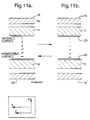
- Figure 7 is a stylised cross section of the device in which a layer 2 of nematic liquid crystal material with positive dielectric anisotropy is contained between a bistable grating surface 25 and a monostable homeotropic surface 26.
- the latter surface 26 could, for example, be a flat photoresist surface coated with lecithin.
- liquid crystal molecules can exist in two stable states. In state (a) both surfaces 25, 26 are homeotropic whereas in (b) the grating surface 25 is in its low pretilt state leading to a splayed structure.
- One particular cell consisted of a layer of nematic ZL12293 (Merck) sandwiched between a bistable grating surface and a homeotropic flat surface. The cell thickness was 3 ⁇ m. Transmission was measured through the cell during the application of dc pulses at room temperature (20°C). The polariser and analyser 13, 13' on each side of the cell 1 were crossed with respect to each other and oriented at ⁇ 45° to the grating grooves. In this set up, the two states in Figure 7, (a) and (b), appear black and white respectively when addressed as follows.
- Figure 8 shows the applied voltage pulses (lower trace) and the optical response (upper trace) as a function of time. Each pulse had a peak height of 55.0 volts and a duration of 3.3ms. Pulse separation was 300ms.
- a second positive pulse causes a transient change in transmission due to the rms effect of coupling to the positive dielectric anisotropy causing a momentary switching of the bulk material to state (a). However, in this case the cell does not latch at the surface and so remains in state (b)..
- the next pulse is negative in sign and so switches the cell from state (b) to state (a).
- the switching occurs across a wide temperature range. As the temperature is increased the voltage required for switching falls. For example at 30°C, a voltage of 44.8 V is required for bistable switching whereas at 50°C the voltage in only 28.8 V. Similarly, for a fixed voltage the required pulse length for latching decreases with temperature.
- FIG. 9 shows one particular example of such a scheme.
- pixels in four consecutive rows R1, R2, R3, R4 in one column are to be switched.
- Two possible alignment states may be arbitrarily defined as ON and OFF states.
- Rows R1 and R4 are to switched to an ON state, rows R2 and R3 are in the OFF state.
- Strobe pulses of +V s for three time slots followed by -V s for 3 time slots (ts) are applied to each row in turn.
- a data waveform is applied to the column as shown and comprises a -V d for 1 ts followed by a +V d for 1 ts for and ON pixel, and -V d for 1 ts followed by +V d for 1 ts for and OFF pixel.
- the resultant waveform consists of large positive and negative pulses which disrupt the nematic orientation and raises its energy up to the barrier that separates the two bistable surface states.
- the liquid crystal molecules align along the electric field as in conventional monostable nematic devices, and as shown in Figure 7a.
- These large 'reset' pulses of opposite polarity are followed immediately by a smaller pulse which is still large enough to dictate the final selection state of the pixel during the relaxation of the orientation.
- Electrical balance is achieved by a small pulse of polarity opposite to the switching pulse and preceding the two large pulses.
- polarity inversion in adjacent display address time may be used.
- the above bistable device achieves final state selection by virtue of the flexoelectric polarisation in one state. Therefore this configuration must contain splay.
- this configuration must contain splay.
- one surface is allowed to switch but working devices can also be made in which both surfaces switch.
- the only remaining constraint is that the low pretilt states on each surface should differ in value so that a finite splay remains.
- the cell can still be switched if it contains a two frequency nematic material, that is a material whose dielectric anisotropy is positive at low frequencies and negative at high frequencies.
- TX2A Merck
- Figure 9 shows a cross section of this configuration.
- a second example of a bistable device is now described.
- a piece of ITO coated glass to form the cell wall was cleaned with acetone and isopropanol and was then spin coated with photoresist (Shipley 1813) at 3000 rpm for 30 seconds giving a coating thickness of 1.5 ⁇ m.
- Softbaking was then carried out at 90°C for 30 minutes.
- a contact exposure was then carried out using a chrome mask containing 0.5pm lines and 0.5 ⁇ m gaps (hence an overall pitch of 1 ⁇ m). In this example the exposure was carried out at normal incidence. Exposure in this geometry leads to a symmetric intensity distribution and therefore a symmetric grating profile. Samples were exposed to light from a mercury lamp (Osram Hg/100) with an intensity of 0.8mW/cm 2 .
- the sample was released from the mask and developed in Shipley MF319 for 20 seconds followed by a rinse in de-ionised water. This left the sample patterned with a symmetric surface modulation.
- the photoresist was then hardened by exposure to deep UV radiation (254nm) followed by baking at 160°C for 45 minutes. This was done to ensure insolubility of the photoresist in the liquid crystal. Finally the grating surface is treated with a solution of a chrome complex surfactant in order to induce a homeotropic boundary condition.
- the cell was oriented between crossed polarisers so that the groove direction was at 45° to the polariser directions.
- state (a) was the bright state while state (b) was the dark state.
- Monopolar pulses of alternating sign were then applied to the cell.
- the pulse length was set to 5.4ms with a 1s pulse separation. Full switching occurred between state (a) and (b) when the peak voltage of the applied pulses was increased to 20.3 V. Pairs of pulses were also applied to the cell in a similar manner to the data shown in Figure 8. Once again only the first pulse changed the state of the system while the second pulse only induced a non-latching transient response. In this case the optical response times were also measured.
- ⁇ n av will be larger for the configuration shown in Figure 10 compared to Figure 7, hence the cell thickness can be less and therefore the optical switching speed will be larger.
- the use of a two frequency nematic limits the choice of available materials, also leads to a more complex addressing scheme, but may allow lower voltage operation.
- the bistable grating surface can also be constructed opposite a planar surface.
- One such cell consisted of a grating with the same profile to that described in example 2. This was constructed opposite a rubbed polymer surface formed using a layer of P132 polyimide (Ciba Geigy). The rubbing direction on the polyimide surface was set parallel to the grating groove direction on the grating surface. The cell gap was set to 2.5 ⁇ m and nematic E7 was used to fill the cell. Cooling to room temperature after filling revealed two states which are shown schematically in Figure 11. This Figure differs from Figure 7 in that the groove direction on the bistable surface is now in the plane of the page (in an x,y plane).
- the 90° pretilt state on the grating forms the hybrid structure shown in (a') while the 0° pretilt state on the grating forms the twisted structure shown in (b').
- the cell was placed in-between crossed polarisers 13, 13' oriented so that the grating grooves (and rubbing direction) were parallel to one polariser, although the polarisers may be rotated to optimise contrast in the two switch states.
- state (b') was the bright state while state (a') was the dark state.
- switching between (a') and (b') occurred at a peak voltage of 56.7 V.
- the optical response times were 110ms for switching from (a') to (b') and 1.4ms for switching from (b) to (a').
- the bright state (b') has a bulk twist of 90°.
- a cholesteric dopant (eg ⁇ 1% of CB15 Merck) may be added to prevent twist disclinations.
- these disclinations may be prevented by arranging the groove directions non parallel to the rubbing alignment directions, eg about 5° adjustment.
- the grating surfaces for these devices can be fabricated using a variety of techniques as listed earlier.
- the homeotropic treatment can be any surfactant which has good adhesion to the grating surface. This treatment should also lead to an unpinned alignment. That is, an alignment which favours a particular nematic orientation without inducing rigid positional ordering of the nematic on the surface.
- the grating modulation has to possess a certain h/w for a given asymmetry for bistability to exist.
- the absolute scale of the modulation is limited by other factors. If the groove depth and pitch are too large then diffractive effects will be significant and lead to loss of device throughput. Furthermore if the groove depth is similar to the cell thickness then the proximity of the groove peaks to the opposite flat surface may inhibit bistable switching. If two gratings are required as in the device shown in Figure 10 then a large groove depth compared to cell thickness would inevitably lead to switching which depends on the phase of the two modulations. This would severely complicate the device manufacturing process.
- a dichroic dye may be incorporated into the liquid crystal material This may be used with or without a polariser, to provide colour, to improve contrast, or to operate as a guest host type device; e.g. the material D124 in E63 (Merck).
- the polariser(s) of the device (with or without a dye) may be rotated to optimise contrast between the two switched states of the device.
Landscapes
- Physics & Mathematics (AREA)
- Nonlinear Science (AREA)
- Chemical & Material Sciences (AREA)
- Crystallography & Structural Chemistry (AREA)
- General Physics & Mathematics (AREA)
- Optics & Photonics (AREA)
- Spectroscopy & Molecular Physics (AREA)
- Mathematical Physics (AREA)
- Liquid Crystal (AREA)
- Liquid Crystal Substances (AREA)
Applications Claiming Priority (3)
| Application Number | Priority Date | Filing Date | Title |
|---|---|---|---|
| GBGB9521106.6A GB9521106D0 (en) | 1995-10-16 | 1995-10-16 | Bistable nematic liquid crystal device |
| GB9521106 | 1995-10-16 | ||
| PCT/GB1996/002463 WO1997014990A1 (en) | 1995-10-16 | 1996-10-09 | Bistable nematic liquid crystal device |
Publications (2)
| Publication Number | Publication Date |
|---|---|
| EP0856164A1 EP0856164A1 (en) | 1998-08-05 |
| EP0856164B1 true EP0856164B1 (en) | 2001-03-28 |
Family
ID=10782334
Family Applications (1)
| Application Number | Title | Priority Date | Filing Date |
|---|---|---|---|
| EP96932739A Expired - Lifetime EP0856164B1 (en) | 1995-10-16 | 1996-10-09 | Bistable nematic liquid crystal device |
Country Status (11)
| Country | Link |
|---|---|
| US (4) | US6249332B1 (enExample) |
| EP (1) | EP0856164B1 (enExample) |
| JP (1) | JP3596897B2 (enExample) |
| KR (1) | KR100352052B1 (enExample) |
| CN (3) | CN1149436C (enExample) |
| AT (1) | ATE200154T1 (enExample) |
| DE (1) | DE69612295T2 (enExample) |
| ES (1) | ES2155205T3 (enExample) |
| GB (2) | GB9521106D0 (enExample) |
| MY (1) | MY120509A (enExample) |
| WO (1) | WO1997014990A1 (enExample) |
Families Citing this family (72)
| Publication number | Priority date | Publication date | Assignee | Title |
|---|---|---|---|---|
| GB9521106D0 (en) * | 1995-10-16 | 1995-12-20 | Secr Defence | Bistable nematic liquid crystal device |
| GB2323956A (en) * | 1997-04-04 | 1998-10-07 | Sharp Kk | Diffractive liquid crystal device |
| GB9713164D0 (en) | 1997-06-23 | 1997-08-27 | Secr Defence | Liquid crystal device |
| JP4278297B2 (ja) | 1997-10-08 | 2009-06-10 | ヒューレット・パッカード・カンパニー | 液晶装置の配向 |
| GB9727142D0 (en) * | 1997-12-24 | 1998-02-25 | Secr Defence | Bistable nematic liquid crystal device |
| GB2345979A (en) | 1999-01-23 | 2000-07-26 | Ibm | High reflectivity bistable liquid crystal display |
| GB9904704D0 (en) | 1999-03-03 | 1999-04-21 | Secr Defence | Addressing bistable nematic liquid crystal devices |
| US6424998B2 (en) | 1999-04-28 | 2002-07-23 | World Theatre, Inc. | System permitting the display of video or still image content on selected displays of an electronic display network according to customer dictates |
| GB9928126D0 (en) | 1999-11-30 | 2000-01-26 | Secr Defence | Bistable nematic liquid crystal device |
| US7460200B2 (en) | 2000-03-27 | 2008-12-02 | Helwett-Packard Development Company, L.P. | Liquid crystal alignment |
| EP1139152A1 (en) * | 2000-03-27 | 2001-10-04 | Hewlett-Packard Company, A Delaware Corporation | Liquid crystal alignment structure |
| EP1139150A1 (en) | 2000-03-27 | 2001-10-04 | Hewlett-Packard Company, A Delaware Corporation | Liquid crystal alignment structure |
| DE60034869T2 (de) * | 2000-03-27 | 2008-02-14 | Hewlett-Packard Co. (N.D.Ges.D.Staates Delaware), Palo Alto | Bistabile nematische Flüssigkristallvorrichtung |
| US20050289015A1 (en) * | 2000-05-17 | 2005-12-29 | Hunter Charles E | System and method permitting merchants to use electronic billboard displays to carry advertisements for products that can be purchased through a universal, automated order processing system |
| GB0017312D0 (en) * | 2000-07-15 | 2000-08-30 | Secr Defence | Bistable liquid crystal devices |
| GB0018629D0 (en) | 2000-07-29 | 2000-09-13 | Secr Defence | Process for making a periodic profile |
| GB0022055D0 (en) | 2000-09-07 | 2000-10-25 | Secr Defence | Addressing multistable nematic liquid crystal devices |
| GB2373062A (en) * | 2001-03-06 | 2002-09-11 | Sharp Kk | Nematic Liquid Crystal Devices |
| GB0114998D0 (en) * | 2001-06-20 | 2001-08-08 | Secr Defence | Liquid crystal device |
| EP1271225A1 (en) | 2001-06-22 | 2003-01-02 | Hewlett-Packard Company, A Delaware Corporation | Bistable nematic liquid crystal device |
| US7015875B2 (en) | 2001-06-29 | 2006-03-21 | Novus Partners Llc | Dynamic device for billboard advertising |
| US7088352B2 (en) | 2002-06-19 | 2006-08-08 | Novus Partners Llc | Dynamic device and method for dispensing machines |
| US7098870B2 (en) | 2001-06-29 | 2006-08-29 | Novus Partners Llc | Advertising method for dynamic billboards |
| US7098869B2 (en) | 2001-06-29 | 2006-08-29 | Novus Partners Llc | Business method for billboard advertising |
| GB2380557A (en) * | 2001-10-02 | 2003-04-09 | Sharp Kk | A liquid crystal display device |
| JP3852342B2 (ja) * | 2002-01-28 | 2006-11-29 | セイコーエプソン株式会社 | 反射板、反射板の製造方法、液晶装置、電子機器 |
| EP1336874B2 (en) | 2002-02-13 | 2013-03-20 | Merck Patent GmbH | Method of preparing a security marking or device comprising an anisotropic polymer film |
| ATE470166T1 (de) | 2002-02-13 | 2010-06-15 | Merck Patent Gmbh | Verfahren zur herstellung von einem anisotropen polymerfilm auf einem substrat mit einer strukturierten oberfläche |
| CN1678948A (zh) * | 2002-03-27 | 2005-10-05 | 艾利丹尼森公司 | 可转换的电-光层压制品 |
| GB0209917D0 (en) | 2002-04-30 | 2002-06-05 | Hewlett Packard Co | Bistable nematic liquid crystal device |
| GB2388201A (en) | 2002-04-30 | 2003-11-05 | Hewlett Packard Co | Liquid crystal device |
| EP1362682A1 (en) * | 2002-05-13 | 2003-11-19 | ZBD Displays Ltd, | Method and apparatus for liquid crystal alignment |
| US20040030111A1 (en) * | 2002-06-19 | 2004-02-12 | Turner Douglas H. | Oligonucleotide directed misfolding of RNA |
| US7551258B2 (en) * | 2002-07-04 | 2009-06-23 | Zbd Displays Limited | Patterned light modulating device |
| AU2003278314A1 (en) * | 2002-10-17 | 2004-05-04 | Zbd Displays Ltd. | Liquid crystal alignment layer |
| FR2847704B1 (fr) * | 2002-11-26 | 2005-01-28 | Nemoptic | Procede et dispositif perfectionnes d'affichage a cristal liquide nematique bistable |
| US7294368B2 (en) * | 2002-12-11 | 2007-11-13 | Merck Patent Gmbh | Liquid crystal composition for use in bistable liquid crystal devices |
| EP1445645A1 (en) * | 2003-02-07 | 2004-08-11 | ZBD Displays Ltd, | Liquid crystal device |
| CN100540631C (zh) * | 2003-05-08 | 2009-09-16 | 默克专利股份有限公司 | 用于双稳态液晶器件的液晶组合物 |
| GB2403023A (en) * | 2003-06-20 | 2004-12-22 | Sharp Kk | Organic light emitting device |
| WO2005040899A1 (en) * | 2003-10-23 | 2005-05-06 | The Hong Kong University Of Science And Technology | Bistable liquid crystal device |
| GB2413646B (en) * | 2004-04-30 | 2008-08-27 | Hewlett Packard Development Co | Bistable nematic liquid crystal display device |
| US7487209B2 (en) * | 2004-07-13 | 2009-02-03 | International Business Machines Corporation | Delivering dynamic media content for collaborators to purposeful devices |
| AU2006205076B2 (en) | 2005-01-10 | 2010-12-23 | Avery Dennison Corporation | Removable curl labels |
| JP4797451B2 (ja) * | 2005-06-01 | 2011-10-19 | ソニー株式会社 | 液晶表示装置 |
| US7965268B2 (en) | 2005-07-08 | 2011-06-21 | Sharp Kabushiki Kaisha | Display device and liquid crystal display panel |
| TW200710519A (en) * | 2005-08-31 | 2007-03-16 | Nat Inst Japan Science & Technology Agency | Liquid crystal display device using nematic liquid crystal |
| WO2007030717A2 (en) * | 2005-09-09 | 2007-03-15 | Wms Gaming Inc. | Wagering game system with bistable lcd display |
| US7427201B2 (en) | 2006-01-12 | 2008-09-23 | Green Cloak Llc | Resonant frequency filtered arrays for discrete addressing of a matrix |
| GB0611141D0 (en) | 2006-06-07 | 2006-07-19 | Univ Strathclyde | Multistable reflective liquid crystal device |
| JP4817380B2 (ja) * | 2006-10-10 | 2011-11-16 | 独立行政法人科学技術振興機構 | 双安定ネマチック液晶表示装置 |
| CN101563432B (zh) | 2006-11-02 | 2014-12-03 | 艾利丹尼森公司 | 用于可洗膜的乳液粘合剂 |
| WO2008097867A1 (en) | 2007-02-07 | 2008-08-14 | Green Cloak Llc | Displays including addressable trace structures |
| US7876385B2 (en) * | 2007-02-27 | 2011-01-25 | Lachezar Komitov | Liquid crystal device |
| ATE554424T1 (de) * | 2007-02-26 | 2012-05-15 | Lachezar Komitov | Flüssigkristallvorrichtung |
| US7832093B2 (en) * | 2007-06-11 | 2010-11-16 | Kent State University | Method of creating an electro-mechanical energy conversion device |
| GB0812770D0 (en) * | 2008-07-11 | 2008-08-20 | Zbd Displays Ltd | A display system |
| EP2414473B1 (en) | 2009-03-30 | 2014-12-31 | Avery Dennison Corporation | Removable adhesive label containing inherently shrinkable polymeric film |
| ES2929654T3 (es) | 2009-03-30 | 2022-11-30 | Avery Dennison Corp | Etiqueta adhesiva despegable que contiene una capa de película polimérica de alto módulo de tracción |
| ES2622956T3 (es) | 2009-03-30 | 2017-07-10 | Avery Dennison Corporation | Etiqueta adhesiva retirable que contiene una capa de película polimérica que tiene afinidad por el agua |
| US9759974B2 (en) | 2011-10-31 | 2017-09-12 | Hewlett-Packard Development Company, L.P. | Liquid crystal display device |
| US9679506B2 (en) | 2012-06-25 | 2017-06-13 | Sharp Kabushiki Kaisha | Multiple function display system |
| US10708575B2 (en) | 2012-06-25 | 2020-07-07 | Sharp Kabushiki Kaisha | Display system with diffuse and specular reflective modes |
| JP6093166B2 (ja) * | 2012-12-06 | 2017-03-08 | スタンレー電気株式会社 | 液晶素子、液晶表示装置 |
| JP6298257B2 (ja) * | 2013-08-21 | 2018-03-20 | スタンレー電気株式会社 | 液晶素子、液晶表示装置 |
| KR101732789B1 (ko) * | 2014-04-04 | 2017-05-08 | 주식회사 엘지화학 | 액정 소자 |
| US10699612B2 (en) | 2014-10-27 | 2020-06-30 | Sharp Kabushiki Kaisha | Display system with specular reflective mode |
| CN108490695B (zh) * | 2018-04-28 | 2024-05-28 | 新辉开科技(深圳)有限公司 | 一种用于电子车牌的液晶显示器 |
| US10823990B2 (en) | 2018-05-16 | 2020-11-03 | Sharp Kabushiki Kaisha | Bistable switchable liquid crystal private device |
| US10670910B2 (en) * | 2018-09-24 | 2020-06-02 | Sharp Kabushiki Kaisha | LCD with four stable and optically distinct states |
| CN116880091B (zh) * | 2019-05-17 | 2026-01-02 | 群创光电股份有限公司 | 电子装置的制造方法 |
| WO2025008433A1 (de) | 2023-07-05 | 2025-01-09 | Eao Ag | Informationsanzeige für einen platz in einem fahrzeug des öffentlichen verkehrs |
Family Cites Families (16)
| Publication number | Priority date | Publication date | Assignee | Title |
|---|---|---|---|---|
| US4333708A (en) * | 1979-11-30 | 1982-06-08 | Bell Telephone Laboratories, Incorporated | Mechanically multistable liquid crystal cell |
| JPS56117217A (en) * | 1980-02-21 | 1981-09-14 | Sharp Corp | Liquid-crystal display recorder |
| US4775225A (en) * | 1985-05-16 | 1988-10-04 | Canon Kabushiki Kaisha | Liquid crystal device having pillar spacers with small base periphery width in direction perpendicular to orientation treatment |
| US4973138A (en) * | 1987-10-27 | 1990-11-27 | Semiconductor Energy Laboratory Co., Ltd. | Liquid crystal device and manufacturing method for the same |
| FR2666923A2 (fr) * | 1990-06-22 | 1992-03-20 | Centre Nat Rech Scient | Perfectionnements aux afficheurs a cristal liquide nematique, a bistabilite de surface, commandes par effet flexoelectrique. |
| JP2877601B2 (ja) * | 1992-01-10 | 1999-03-31 | 松下電器産業株式会社 | 液晶表示装置とその製造法 |
| US5268782A (en) * | 1992-01-16 | 1993-12-07 | Minnesota Mining And Manufacturing Company | Micro-ridged, polymeric liquid crystal display substrate and display device |
| US5384650A (en) * | 1992-04-06 | 1995-01-24 | Hughes Aircraft Company | Light valve with twisted perpendicular liquid crystal with a negative dielectric anisotropy |
| GB9402517D0 (en) * | 1994-02-09 | 1994-03-30 | Secr Defence | Ferroelectric liquid crystal alignment |
| GB9402513D0 (en) * | 1994-02-09 | 1994-03-30 | Secr Defence | Bistable nematic liquid crystal device |
| GB9402492D0 (en) * | 1994-02-09 | 1994-03-30 | Secr Defence | Liquid crystal device alignment |
| GB9502635D0 (en) * | 1995-02-10 | 1995-03-29 | Secr Defence | Liquid crystal device alignment |
| US5831700A (en) * | 1995-05-19 | 1998-11-03 | Kent State University | Polymer stabilized four domain twisted nematic liquid crystal display |
| GB9521106D0 (en) * | 1995-10-16 | 1995-12-20 | Secr Defence | Bistable nematic liquid crystal device |
| GB2348641A (en) * | 1999-04-06 | 2000-10-11 | Secr Defence | Liquid crystal alkenyl compounds incorporating a heterocyclic five-membered ring |
| GB0017953D0 (en) * | 2000-07-21 | 2000-09-13 | Secr Defence | Liquid crystal device |
-
1995
- 1995-10-16 GB GBGB9521106.6A patent/GB9521106D0/en active Pending
-
1996
- 1996-10-09 JP JP51558197A patent/JP3596897B2/ja not_active Expired - Fee Related
- 1996-10-09 KR KR10-1998-0702760A patent/KR100352052B1/ko not_active Expired - Fee Related
- 1996-10-09 EP EP96932739A patent/EP0856164B1/en not_active Expired - Lifetime
- 1996-10-09 DE DE69612295T patent/DE69612295T2/de not_active Expired - Lifetime
- 1996-10-09 US US09/043,788 patent/US6249332B1/en not_active Expired - Lifetime
- 1996-10-09 AT AT96932739T patent/ATE200154T1/de active
- 1996-10-09 CN CNB961976489A patent/CN1149436C/zh not_active Expired - Lifetime
- 1996-10-09 CN CN2006101001721A patent/CN1928684B/zh not_active Expired - Fee Related
- 1996-10-09 ES ES96932739T patent/ES2155205T3/es not_active Expired - Lifetime
- 1996-10-09 WO PCT/GB1996/002463 patent/WO1997014990A1/en not_active Ceased
- 1996-10-09 CN CNB2004100304681A patent/CN1303464C/zh not_active Expired - Fee Related
- 1996-10-09 GB GB9802806A patent/GB2318422B/en not_active Expired - Fee Related
- 1996-10-16 MY MYPI96004294A patent/MY120509A/en unknown
-
2000
- 2000-12-20 US US09/740,260 patent/US6456348B2/en not_active Expired - Lifetime
-
2002
- 2002-08-06 US US10/212,141 patent/US6714273B2/en not_active Expired - Fee Related
-
2004
- 2004-02-11 US US10/775,342 patent/US7280175B2/en not_active Expired - Fee Related
Also Published As
| Publication number | Publication date |
|---|---|
| US20050062919A1 (en) | 2005-03-24 |
| US6249332B1 (en) | 2001-06-19 |
| HK1069640A1 (en) | 2005-05-27 |
| CN1529203A (zh) | 2004-09-15 |
| GB9521106D0 (en) | 1995-12-20 |
| US6714273B2 (en) | 2004-03-30 |
| CN1928684A (zh) | 2007-03-14 |
| CN1200180A (zh) | 1998-11-25 |
| ATE200154T1 (de) | 2001-04-15 |
| HK1103452A1 (en) | 2007-12-21 |
| CN1149436C (zh) | 2004-05-12 |
| GB2318422B (en) | 1999-07-21 |
| ES2155205T3 (es) | 2001-05-01 |
| KR100352052B1 (ko) | 2003-04-10 |
| GB2318422A (en) | 1998-04-22 |
| JPH11513809A (ja) | 1999-11-24 |
| JP3596897B2 (ja) | 2004-12-02 |
| MY120509A (en) | 2005-11-30 |
| CN1928684B (zh) | 2010-12-22 |
| HK1015469A1 (en) | 1999-10-15 |
| DE69612295T2 (de) | 2001-08-23 |
| GB9802806D0 (en) | 1998-04-08 |
| KR19990064269A (ko) | 1999-07-26 |
| EP0856164A1 (en) | 1998-08-05 |
| US20010028426A1 (en) | 2001-10-11 |
| DE69612295D1 (de) | 2001-05-03 |
| CN1303464C (zh) | 2007-03-07 |
| WO1997014990A1 (en) | 1997-04-24 |
| US7280175B2 (en) | 2007-10-09 |
| US20030063246A1 (en) | 2003-04-03 |
| US6456348B2 (en) | 2002-09-24 |
Similar Documents
| Publication | Publication Date | Title |
|---|---|---|
| EP0856164B1 (en) | Bistable nematic liquid crystal device | |
| EP0744041B1 (en) | Bistable nematic liquid crystal device | |
| EP1042702B1 (en) | Bistable nematic liquid crystal device | |
| EP0808476B1 (en) | Liquid crystal device alignment | |
| EP0744040B1 (en) | Ferroelectric liquid crystal device alignment | |
| CA2182963A1 (en) | Liquid crystal device alignment | |
| EP0619030A1 (en) | Ferroelectric liquid crystal display device | |
| Armitage | Liquid-crystal display device fundamentals | |
| HK1103452B (en) | Bistable nematic liquid crystal device | |
| HK1015469B (en) | Bistable nematic liquid crystal device | |
| HK1069640B (en) | Bistable nematic liquid crystal device | |
| HK1033365A (en) | Bistable nematic liquid crystal device |
Legal Events
| Date | Code | Title | Description |
|---|---|---|---|
| PUAI | Public reference made under article 153(3) epc to a published international application that has entered the european phase |
Free format text: ORIGINAL CODE: 0009012 |
|
| 17P | Request for examination filed |
Effective date: 19980213 |
|
| AK | Designated contracting states |
Kind code of ref document: A1 Designated state(s): AT BE CH DE ES FR GB IT LI NL |
|
| GRAG | Despatch of communication of intention to grant |
Free format text: ORIGINAL CODE: EPIDOS AGRA |
|
| 17Q | First examination report despatched |
Effective date: 20000630 |
|
| GRAG | Despatch of communication of intention to grant |
Free format text: ORIGINAL CODE: EPIDOS AGRA |
|
| GRAH | Despatch of communication of intention to grant a patent |
Free format text: ORIGINAL CODE: EPIDOS IGRA |
|
| GRAH | Despatch of communication of intention to grant a patent |
Free format text: ORIGINAL CODE: EPIDOS IGRA |
|
| GRAA | (expected) grant |
Free format text: ORIGINAL CODE: 0009210 |
|
| ITF | It: translation for a ep patent filed | ||
| AK | Designated contracting states |
Kind code of ref document: B1 Designated state(s): AT BE CH DE ES FR GB IT LI NL |
|
| REF | Corresponds to: |
Ref document number: 200154 Country of ref document: AT Date of ref document: 20010415 Kind code of ref document: T |
|
| REG | Reference to a national code |
Ref country code: CH Ref legal event code: EP |
|
| REG | Reference to a national code |
Ref country code: ES Ref legal event code: FG2A Ref document number: 2155205 Country of ref document: ES Kind code of ref document: T3 |
|
| REF | Corresponds to: |
Ref document number: 69612295 Country of ref document: DE Date of ref document: 20010503 |
|
| ET | Fr: translation filed | ||
| REG | Reference to a national code |
Ref country code: CH Ref legal event code: NV Representative=s name: E. BLUM & CO. PATENTANWAELTE |
|
| RAP2 | Party data changed (patent owner data changed or rights of a patent transferred) |
Owner name: QINETIQ LIMITED |
|
| NLT2 | Nl: modifications (of names), taken from the european patent patent bulletin |
Owner name: QINETIQ LIMITED |
|
| BECA | Be: change of holder's address |
Free format text: 20011123 *QINETIQ LTD:85 BUCKINGHAM GATE, LONDON SW14 0LX |
|
| REG | Reference to a national code |
Ref country code: GB Ref legal event code: IF02 |
|
| PLBE | No opposition filed within time limit |
Free format text: ORIGINAL CODE: 0009261 |
|
| STAA | Information on the status of an ep patent application or granted ep patent |
Free format text: STATUS: NO OPPOSITION FILED WITHIN TIME LIMIT |
|
| 26N | No opposition filed | ||
| NLS | Nl: assignments of ep-patents |
Owner name: QINETIQ LIMITED |
|
| REG | Reference to a national code |
Ref country code: CH Ref legal event code: PUE Owner name: ZBD DISPLAYS LTD. Free format text: THE SECRETARY OF STATE FOR DEFENCE#DEFENCE EVALUATION AND RESEARCH AGENCY, IVELY ROAD#FARNBOROUGH, HAMPSHIRE GU14 6TD (GB) -TRANSFER TO- ZBD DISPLAYS LTD.#MALVERN HILLS SCIENCE PARK#GERALDINE ROAD, MALVERN, WORCS (GB) |
|
| BECA | Be: change of holder's address |
Owner name: *ZBD DISPLAYS LTDMALVERN HILLS SCIENCE PARK, GERAL Effective date: 20041103 |
|
| NLS | Nl: assignments of ep-patents |
Owner name: ZBD DISPLAYS LIMITED |
|
| REG | Reference to a national code |
Ref country code: FR Ref legal event code: TP |
|
| REG | Reference to a national code |
Ref country code: CH Ref legal event code: PFA Owner name: ZBD DISPLAYS LTD. Free format text: ZBD DISPLAYS LTD.#MALVERN HILLS SCIENCE PARK#GERALDINE ROAD, MALVERN, WORCS (GB) -TRANSFER TO- ZBD DISPLAYS LTD.#MALVERN HILLS SCIENCE PARK#GERALDINE ROAD, MALVERN, WORCS (GB) |
|
| REG | Reference to a national code |
Ref country code: GB Ref legal event code: 732E Free format text: REGISTERED BETWEEN 20110210 AND 20110216 |
|
| PGFP | Annual fee paid to national office [announced via postgrant information from national office to epo] |
Ref country code: CH Payment date: 20131024 Year of fee payment: 18 Ref country code: AT Payment date: 20131024 Year of fee payment: 18 Ref country code: BE Payment date: 20131031 Year of fee payment: 18 Ref country code: FR Payment date: 20131022 Year of fee payment: 18 Ref country code: DE Payment date: 20131025 Year of fee payment: 18 |
|
| PGFP | Annual fee paid to national office [announced via postgrant information from national office to epo] |
Ref country code: ES Payment date: 20131024 Year of fee payment: 18 Ref country code: NL Payment date: 20131024 Year of fee payment: 18 Ref country code: IT Payment date: 20131025 Year of fee payment: 18 |
|
| REG | Reference to a national code |
Ref country code: DE Ref legal event code: R119 Ref document number: 69612295 Country of ref document: DE |
|
| REG | Reference to a national code |
Ref country code: NL Ref legal event code: V1 Effective date: 20150501 |
|
| REG | Reference to a national code |
Ref country code: CH Ref legal event code: PL |
|
| REG | Reference to a national code |
Ref country code: AT Ref legal event code: MM01 Ref document number: 200154 Country of ref document: AT Kind code of ref document: T Effective date: 20141009 |
|
| PG25 | Lapsed in a contracting state [announced via postgrant information from national office to epo] |
Ref country code: BE Free format text: LAPSE BECAUSE OF NON-PAYMENT OF DUE FEES Effective date: 20141031 |
|
| PG25 | Lapsed in a contracting state [announced via postgrant information from national office to epo] |
Ref country code: CH Free format text: LAPSE BECAUSE OF NON-PAYMENT OF DUE FEES Effective date: 20141031 Ref country code: DE Free format text: LAPSE BECAUSE OF NON-PAYMENT OF DUE FEES Effective date: 20150501 Ref country code: LI Free format text: LAPSE BECAUSE OF NON-PAYMENT OF DUE FEES Effective date: 20141031 |
|
| REG | Reference to a national code |
Ref country code: FR Ref legal event code: ST Effective date: 20150630 |
|
| PG25 | Lapsed in a contracting state [announced via postgrant information from national office to epo] |
Ref country code: NL Free format text: LAPSE BECAUSE OF NON-PAYMENT OF DUE FEES Effective date: 20150501 Ref country code: IT Free format text: LAPSE BECAUSE OF NON-PAYMENT OF DUE FEES Effective date: 20141009 Ref country code: AT Free format text: LAPSE BECAUSE OF NON-PAYMENT OF DUE FEES Effective date: 20141009 Ref country code: FR Free format text: LAPSE BECAUSE OF NON-PAYMENT OF DUE FEES Effective date: 20141031 |
|
| REG | Reference to a national code |
Ref country code: ES Ref legal event code: FD2A Effective date: 20151127 |
|
| PGFP | Annual fee paid to national office [announced via postgrant information from national office to epo] |
Ref country code: GB Payment date: 20151026 Year of fee payment: 20 |
|
| PG25 | Lapsed in a contracting state [announced via postgrant information from national office to epo] |
Ref country code: ES Free format text: LAPSE BECAUSE OF NON-PAYMENT OF DUE FEES Effective date: 20141010 |
|
| REG | Reference to a national code |
Ref country code: GB Ref legal event code: PE20 Expiry date: 20161008 |
|
| PG25 | Lapsed in a contracting state [announced via postgrant information from national office to epo] |
Ref country code: GB Free format text: LAPSE BECAUSE OF EXPIRATION OF PROTECTION Effective date: 20161008 |