EP0849684B1 - Rechnerbuserweiterung - Google Patents
Rechnerbuserweiterung Download PDFInfo
- Publication number
- EP0849684B1 EP0849684B1 EP97310178A EP97310178A EP0849684B1 EP 0849684 B1 EP0849684 B1 EP 0849684B1 EP 97310178 A EP97310178 A EP 97310178A EP 97310178 A EP97310178 A EP 97310178A EP 0849684 B1 EP0849684 B1 EP 0849684B1
- Authority
- EP
- European Patent Office
- Prior art keywords
- connector
- line
- bus
- gate
- power
- Prior art date
- Legal status (The legal status is an assumption and is not a legal conclusion. Google has not performed a legal analysis and makes no representation as to the accuracy of the status listed.)
- Expired - Lifetime
Links
Images
Classifications
-
- G—PHYSICS
- G06—COMPUTING OR CALCULATING; COUNTING
- G06F—ELECTRIC DIGITAL DATA PROCESSING
- G06F12/00—Accessing, addressing or allocating within memory systems or architectures
- G06F12/02—Addressing or allocation; Relocation
- G06F12/06—Addressing a physical block of locations, e.g. base addressing, module addressing, memory dedication
- G06F12/0646—Configuration or reconfiguration
- G06F12/0669—Configuration or reconfiguration with decentralised address assignment
- G06F12/0676—Configuration or reconfiguration with decentralised address assignment the address being position dependent
-
- G—PHYSICS
- G06—COMPUTING OR CALCULATING; COUNTING
- G06F—ELECTRIC DIGITAL DATA PROCESSING
- G06F13/00—Interconnection of, or transfer of information or other signals between, memories, input/output devices or central processing units
- G06F13/38—Information transfer, e.g. on bus
- G06F13/40—Bus structure
- G06F13/4063—Device-to-bus coupling
- G06F13/4068—Electrical coupling
- G06F13/4081—Live connection to bus, e.g. hot-plugging
Definitions
- This invention relates to managing an expandable computer bus architecture.
- Open system architectures are well known in computer systems. Open computer system architectures are based on the provision of a computer bus which can be expanded by means of expansion cards. In order to provide for computer bus expansion, on a typical backplane, or motherboard, a computer bus will be provided with a number of sockets into which expansion cards can be inserted. There are a number of different standards for computer bus expansions.
- One conventional standard is the PCI (Peripheral Component Interface) architecture.
- the PCI architecture enables a bus to be expanded by the insertion of cards, but the standard PCI architecture is less than ideal for a highly reliable system for a number of reasons. Firstly, PCI cards are not hot replaceable, meaning that the cards cannot be inserted when the system is actually running.
- European patent application EP-A-0,632,393 describes an apparatus and a method of connecting an IC card to a motherboard. On detecting that an IC card has been inserted into a connector located on the motherboard, a power bus of and a general signal bus of the motherboard are connected to a power bus and a general signal bus of the IC card, respectively. A connector circuit located on the motherboard between the motherboard power bus and the connector and between the motherboard general signal bus and the connector controls the making of the connections.
- European patent application EP-A-0,811,932 and International application WO 93/15459 also describe similar switch circuitry on a motherboard for selectively connecting bus lines on the motherboard to a connector for receiving a circuit card.
- One aspect of the invention provides multi-contact connector for the connection of an expansion card to a computer backplane, said connector comprising a gate electrically connected in-line between a line connector pin for connection to a line on a said backplane and a line contact for connection to a corresponding line contact on an inserted expansion card, a gate signal input of said gate being electrically connected to a gate signal connector pin for connection to a gate signal line on a said backplane
- a gate in the connector between the bus line and the connector contact enables control of the input/output to a card inserted or to be inserted in the connector.
- the contact can be enabled selectively, for example continuously from some predetermined time or for a particular bus cycle.
- This control provides a basis for enabling hot insertion and removal of a card for a running system, in that the appropriate contacts can be disabled, preventing bus errors and card malfunctions.
- a PCI bus controller on the backplane is to be provided, standard cold-insertable PCI cards can be used.
- a plurality of transmission gates (for example implemented by a pair of FETs) can be provided, each electrically connected in-line between a respective connector pin for connection to a line on a backplane and a respective contact for connection to a corresponding contact on an inserted expansion card.
- Respective gate signal inputs for each of transmission gates are electrically connected to a common connector pin for connection to a gate signal line.
- the connector can also comprise a switch gate (for example implemented by an FET) electrically connected in-line between a connector pin for connection to a power line on a backplane and a contact for connection to a corresponding power contact on an inserted expansion card, a control input of the switch gate being electrically connected to a connector pin for connection to a power signal line.
- a switch gate for example implemented by an FET
- Another aspect of the invention provides a backplane for a computer system, the backplane having mounted thereon at least one such multi-contact connector for expansion cards, at least one bus line for connection to a predetermined line contact of said connector(s) and a gate signal line for supplying a gate signal to said gate signal connector pin.
- a respective gate signal line can be provided for each of a plurality of connectors, whereby selective control of the gates for respective connectors can be provided. This further enables dynamic cycle switching of the cards to be achieved.
- the bus can comprise a plurality of data lines for connection to respective data contacts of a connector, a respective transmission gate (preferably implemented by a pair of FETs - field effect transistors) being provided between each data line and the respective contact of the connector, thereby enabling selective gating of the data and address signals to and from a connected card.
- a respective gate signal line can be provided for each of a plurality of connectors, with the gate signal being supplied in parallel to each transmission gate of a connector.
- a plurality of gate signal lines can be provided for a connector so that individual transmission gates can be enabled at timings selected for the lines concerned.
- At least one power line can be provided for connection to a power contact of the connector(s), a switch gate (preferably implemented by an FET) being connected between the power line and the power contact of a connector and a power signal line for supplying a power control signal to control the switch gate.
- a switch gate preferably implemented by an FET
- At least one bus request line can be connected to a bus request contact of a connector and a bus request gate for selectively passing the bus request signal from the bus request connector to the bus request line.
- the bus request gate can be operable in use to pass a bus request signal only after a predetermined delay following power being supplied to a card connected to the connector. In this way, it is possible to allow for the circuits of card to settle after application of power to the card, avoiding transients and other false signals from disrupting the operation of a computer system incorporating the backplane.
- the gate signal line can be implemented using a strobe line common to each connector, the strobe line being active, in use, as the gate line when a radial address signal on a radial address signal line for the connector is active.
- a further aspect of the invention provides a computer system comprising such a backplane and a bus controller connected to said bus line for data transmission and connected to said gate signal line for supplying a gate signal for said gate.
- the bus controller can selectively supply a gate signal in parallel to each transmission gate of only one connector for a given bus cycle for enabling the transmissions gates of the connector for the given bus cycle, whereby dynamic cycle switching can be provided.
- the bus controller can selectively apply a power control signal on the power control signal line when a card has been inserted in the connector.
- the bus controller can comprise an address decoder providing geographic decoding of address signals for respective cards, whereby the bus controller can determine in advance the source of a response to any bus cycle before the bus cycle commences.
- an embodiment of the invention can provide a method of configuring a PCI bus mechanism to provide geographic addressing of cards connected to the bus, whereby the bus controller can determine in advance the source of a response to any bus cycle before the bus cycle commences.
- Geographic addressing in a PCI context overcomes the difficulty of prior PCI implementations in which the isolation of faults on a PCI bus is difficult and time consuming. As the bus controller can determine in advance the source of a response to any bus cycle before the bus cycle commences, the location of a faulty card can be readily identified.
- Another aspect of the invention provides a method of connecting an expansion card to a backplane of a computer system, said method comprising steps of: inserting an expansion card into a multi-contact connector as described above for said expansion card; and subsequently enabling said gate by supplying a gate signal on a gate signal line to said gate.
- the method can include the hot-insertion of the card into the multi-contact connector.
- the bus controller preferably supplies a gate signal for enabling the transmission gates of only one connector for a given bus cycle.
- the method can include a further step between the insertion step and the enabling step of: supplying a power supply signal to a power switch connected between a power line and a power contact of the connector when the card has been inserted in the connector, whereby power is supplied to the card only after insertion, thereby providing dynamic cycle switching.
- the method can also include a further step after the step of supplying a power signal of: enabling a bus request signal to be passed from a bus request contact of the connector only after a predetermined delay following the supply of power to the card.
- a method of an embodiment of the invention employs geographic addressing by a bus controller to cards connected to the computer system, whereby the bus controller can determine in advance the source of a response to any bus cycle before the bus cycle commences.
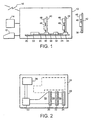
- FIG. 1 is a schematic cross-section of a computer system 10, which comprises of a backplane, or motherboard, or main board 20.
- a backplane or motherboard, or main board 20.
- FIG. 1 is a schematic cross-section of a computer system 10, which comprises of a backplane, or motherboard, or main board 20.
- a backplane it should be understood that the reference to a backplane is intended to relate to a board or other carrier plane on which at least one bus is provided, and to which at least one expansion, or additional card can be connected via a connector, or socket.
- a bus controller 22 is represented schematically on the backplane 20.
- the bus controller 22 is connected via a bus 24 to a plurality of sockets, or connectors, 30, 32 and 34.
- Each of the connectors 30, 32 and 34 is provided with a plurality of contacts for making contact with corresponding contacts on an insertable card.
- two cards 40 and 44 are shown inserted in the connectors 30 and 34, respectively.
- the individual cards 40 and 44 are provided with electronic circuits and or other components 46 which are connected by printed circuit or other wiring 48 to connectors provided at one edge of the card, either directly at the edge on the card or by means of a separate connector (not shown).
- the connector 32 is not populated in Figure 1.
- a further card, 42 could also be inserted in the connector 32 to expand the computer system 10.
- Figure 1 also illustrates the card 42 provided with circuits 46, connected by printed circuit wiring 48 to an edge connector 38.
- Figure 2 is a schematic plan view of the backplane 20 illustrated in side view in Figure 1.
- Figure 2 is a schematic diagram showing only those components relevant to the description of the present invention.
- Figure 2 schematically shows a processor 26 connected to the bus controller 22 and schematically shows additional circuitry 28.
- the computer system 10 can include any normal configuration of a computer system with additional circuitry including timing circuitry, control circuitry, data storage devices, etc.
- data entry and output devices such as a keyboard 12 and display 14 can form part of the computer system 10, as can a connection to a network 16, etc.
- Some of the connections to external devices such as a display 14, or an external network, can be provided by means of the circuitry on one of the insertable cards, or alternatively such interfaces can be provided from the backplane circuitry 28 in a manner which will be immediately apparent to one skilled in the art.
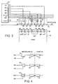
- the bus 24 shown schematically in Figures 1 and 2 comprises many different signal lines. Some of the signal lines of a bus in accordance with the present invention are shown in Figure 3. Some of the bus signal lines for connection to the insertable cards are required permanently. Such signals include, for example, power and clock signals and output signals such as a bus request signal which needs to be observed permanently. Other signals only need to be observed when a card carries out a data transaction during an appropriate bus cycle, for example data bus signals. An embodiment of the present invention can take account of this.
- FIG 3 a number of contacts 50, 54, 56, 60 and 64 in a connector 32 are illustrated schematically. These are for connection to respective contacts on a card 42.
- Figure 4 illustrates in more detail selected ones of the contacts shown in Figure 3.
- contact 50 in the connector 40 on the backplane 20 is connected to a bus line Vcc for supplying a power supply to the power supply contact 70 of an inserted card 42.
- the connector 40 or the backplane 20 is provided with a switch gate 52 (which is preferably configured as a field effect transistor) which is switched in response to a power enable PE signal also supplied over the backplane 20 from the bus controller 22.
- a contact 60 receives a bus request signal BR from a corresponding contact 80 of an inserted card 42.
- the bus request contact 60 is connected to a bus request line BR to the bus controller 22 via a bus request gate 62 which, as shown in Figure 4, can be made to be responsive to the power enable signal PE.
- the bus request gate 62 can be arranged to provide a delay after receipt of the power enable signal before enabling bus request signals to be passed from the contact 60 to the bus request line BR. The delay is set in order to give sufficient time for the circuitry on the card 42 to stabilise.
- the power enable signal PE is supplied for switching the switch 52 and for enabling the delay period to be commenced when it is detected, or the user signals, that the card 42 has been correctly inserted within the connector 32.
- bus request gate 62 it may be preferable to implement the bus request gate 62 as a simple gate operated under software control.
- a plurality of connectors 56 for data and address lines are provided.
- Each of the data/address contacts 56 is connected to a corresponding data/address line D/A on the backplane bus via a respective transmission gate 54.
- the transmission gates 58 are enabled by a gate enable signal GE, provided from the bus controller 22.
- FIG. 3 Also shown in Figure 3 is a ground contact 54 connected to a grounding line and a card enable contact 64 connected to a card enable line CE from the bus controller 22.
- Corresponding contacts 54 and 84 are provided on the card 42. It will be appreciated that additional contacts can be provided on the connector 32 and on the card 42 for additional signal lines as required by any particular implementation.
- Each of the contacts 70, 74, 76, 80 and 84 on the card 42 are connected to printed circuit or other wiring Vcc, G, D/A, BR, CE on the card 42 for connection to the appropriate functional units on that card.
- the data/address lines D/A are provided in parallel to each of the connectors 30, 32 and 34.
- the power and ground lines Vcc and G are provided in parallel to the connectors 30, 32 and 34.
- Separate bus requests, gate enable, power enable and card enable lines are provided to each of the respective connectors 30, 32 and 34.
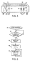
- FIG. 5 is a schematic representation of a connector for use on a backplane, which connector includes the various gates described with reference to Figure 4.
- a switch gate 52 here a FET
- the control signal PE is supplied via a PE pin.
- the PE signal is also supplied to a delay circuit 62 which is provided between a contact 60 and a pin BR.
- a plurality of transmission gates 58 are provided in line between data/address contact 60 and D/A pins.
- the control input for each transmission gate 58 is connected to a GE pin. It will be appreciated that Figure 5 is merely schematic and only illustrates selected pins. In practice, many more pins would be provided, and the connector may take on any standard or alternative connector configurations.
- the switch 52 and the transmission gates 58 would be provided in the connector, in alternative embodiments, other configurations of gates could be provided within the connector, subject to there being at least selected gates connected between critical contacts of the connector and corresponding pins for connection to printed circuit or other wiring on the backplane.
- Figure 6 is a flow diagram for schematically illustrating the selective enabling of the various contacts in the connector 32 when the card 42 is inserted.
- the process is initiated by the user inserting the edge connector 38 of the card 42 into the connector 32 on the backplane 20.
- a mechanism is provided 92 for detecting correct insertion of the card. This could be performed by the user inputting appropriate data into the computer 10 to confirm that the card has been correctly inserted.
- automatic means could be provided for detecting the correct insertion of the card. Optionally, this could be by sensing a particular signal level at a contact 66, which on insertion of the card 42 makes contact with the further contact 86 on the card, over a line (e.g. an acknowledge line ACK) to the controller 22.
- a mechanical sensor could be provided to detect the correct insertion of the card connector 38 in the backplane connector 32.
- impedance values on an existing line could be used to detect correct insertion of the card.
- a power supply signal PE is supplied at 94 from the bus controller 22 to the switch 54 for enabling power 50 to be supplied to the card 42. This ensures that power is not supplied until all the appropriate connections have been made.
- the power enable PE signal is also supplied to the delay stage 62 to prevent bus request signals being received by the bus controller 22 from the insert card 42 until circuitry on that card has stabilised. This ensures that spurious bus request signals and/or other spikes are not sent to the bus controller 22.
- the card When the bus request signal line has been enabled in step 96, the card is then fully operational and the power supply, clock and other permanently required signals are available permanently to the card 42. Also, the bus request line from the card is permanently monitored.
- the data/address contacts 56 of the connector 32 are only enabled at appropriate bus cycle times for the card 42 in question, thus providing dynamic cycle switching.
- two mechanisms are employed by the bus controller 22 for determining when the data/address contacts 56 are enabled for a particular card 42.
- the first mechanism is to enable the data/address contacts 56 by supplying a gate enable signal to the appropriate transmissions gates 58 when the card 42 in question when the controller grants the bus to the card in response to the card asserting the bus request line for that card. It will be noted that there is one bus request line on the backplane 20 for each card connector 30, 32, 34 etc. Accordingly, the bus controller 22 knows immediately which card has asserted respective bus request lines, enables the appropriate transmission gates 58 by supplying an appropriate gate enable signal to the card in question at the same time as granting bus access during the appropriate bus cycle.
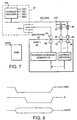
- FIG. 7 An alternative mechanism as represented in Figure 7 is employed when the card in question is operating in the slave mode under the control of the controller 22.
- the card controller 22 employs geographic addressing to address the individual cards. This achieved by employing programmable addressing (for example as provided in accordance with the PCI standard).
- programmable addressing for example as provided in accordance with the PCI standard.
- the bus controller 22 is provided with an address decoder 100 which is responsive to an address on address lines 102 to generate the gate enable signals GE0-GE3 for (in this case) up to four separate cards (it will be remembered that only three card connectors are shown and therefore only three card enable signals are needed, by way of example, in Figure 1).
- the bus controller 22 can thereby determine in advance the source of a response (acknowledgement ACK) to any cycle before the bus cycle commences, thereby enabling ready identification of a faulty card.
- the power enable signals and also the card enable signals are preferably provided under software control.
- Figure 3 illustrates a particular configuration of lines in Figure 3, it will be appreciated that this is merely one example of a possible line configuration for the backplane bus and the connectors 32/38. Alternative detailed configuration of bus lines can be provided. Also, it is possible for example, to provide the gate enable signals without the provision of separate gate enable lines on the backplane bus.
- Figure 8 illustrates the use of a radial address line, RAD, which would be provided separately for each of the individual connectors 32 and a common strobe to determine the timing of the opening of the transmission gates 58.
- the strobe signal is supplied in common to all the cards, this could be used in combination with the selectively addressed RAD signal to ensure that the transmission gates for a particular card are enabled during the appropriate cycle for that card.
- An embodiment of the invention can isolate each connector of a bus (for example PCI bus) by the placing of transmission gates (for example configured as field effect transistors) on the backplane between PCI bus connectors.
- the transmission gates can be provided as an integral component in a connector for the insertion of a backplane card or could be provided on the backplane bus itself.
- An embodiment of the invention can enable rapid and reliable fault detection through the use of geographical decoding of the bus addresses whereby the bus controller will know immediately which connector (slot) has a bus connected to it in which a fault has occurred as the bus controller will know in advance which card will respond to any cycle before that cycle issues.
- the overall effective transmission line over the backplane bus is reduced to the line length on the backplane plus the transmission line length on the selected card. This provides significant transmission line advantages enabling reduced electromagnetic interference, and reliable higher frequency operation.
- fault isolation becomes much easier as a fault, for example a short on a bus line bit, will only manifest itself when the transmission gates for the faulty card are enabled. It will be appreciated that fault isolation is therefore facilitated.
- the additional backplane transistor isolation provided for power supply lines, clocks, etc are a preferred embodiment of the invention, which are enabled when the card is turned on and are kept enabled until it is turned off. In a preferred embodiment of the invention as described herein, a number of advantages are provided.
Landscapes
- Engineering & Computer Science (AREA)
- Theoretical Computer Science (AREA)
- General Engineering & Computer Science (AREA)
- Physics & Mathematics (AREA)
- General Physics & Mathematics (AREA)
- Computer Hardware Design (AREA)
- Power Sources (AREA)
- Debugging And Monitoring (AREA)
- Coupling Device And Connection With Printed Circuit (AREA)
- Information Transfer Systems (AREA)
Claims (31)
- Anschluß (32) mit mehreren Kontakten für die Verbindung einer Erweiterungskarte (42) mit der Hauptplatine (20) eines Computers, wobei der Anschluß ein Gatter (58) aufweist, welches elektrisch in eine Leitung zwischen einen Leitungsanschlußstift (D/A) für die Verbindung mit einer Leitung auf der Hauptplatine des Computers und einen Leitungskontakt (56) für die Verbindung mit einem entsprechenden Leitungsanschluß (76) auf einer eingesteckten Erweiterungskarte geschaltet ist, wobei ein Gattersignaleingang des Gatters mit einem Anschlußstift (GE) für das Gattersignal verbunden ist für die Verbindung mit einer Gattersignalleitung auf der Hauptplatine des Computers.
- Anschluß nach Anspruch 1, welcher eine Mehrzahl von Gattern aufweist, wobei jedes elektrisch in die Leitung zwischen einen entsprechenden Leitungsanschlußstift und einen entsprechenden Leitungskontakt geschaltet ist für die Verbindung mit einem entsprechendem Leitungskontakt auf einer eingesetzten Erweiterungskarte.
- Anschluß nach Anspruch 2, wobei die jeweiligen Gattersignaleingänge für jedes der Gatter elektrisch mit einem gemeinsamen Gattersignalanschlußstift verbunden sind für den Anschluß an einer Gattersignalleitung.
- Anschluß nach Anspruch 2, wobei die jeweiligen Gattersignaleingänge für jedes der Gatter elektrisch mit getrennten Gattersignalanschlußstiften für die Verbindung mit entsprechenden Gattersignalleitungen verbunden sind.
- Anschluß nach einem der Ansprüche 1 bis 4, welcher zusätzlich einen Schalter (52) aufweist, der elektrisch in die Leitung zwischen einen Anschlußstift (Vcc) für eine Stromversorgungsleitung für die Verbindung mit einer Stromversorgungsleitung auf der Hauptplatine und einen Stromversorgungsleitungskontakt (50) für den Anschluß mit einem entsprechenden. Leitungskontakt (70) der Stromversorgung auf einer eingesetzten Erweiterungskarte geschaltet ist, wobei ein Steuerungseingang des Schaltgatters elektrisch mit einem Steuersignalanschlußstift (PE) für die Verbindung mit einer Steuersignalleitung der Stromversorgung verbunden ist.
- Anschluß nach einem der Ansprüche 1 bis 5, welcher zusätzlich ein Busanforderungsgatter (62) aufweist, welches elektrisch in die Leitung zwischen den Kontakt (60) einer Busanforderungsleitung für die Verbindung mit einem entsprechenden Kontakt (80) einer Busanforderungsleitung auf einer eingesetzten Erweiterungskarte und einen Anschlußstift (BR) einer Busanforderungsleitung für die Verbindung mit einer Busanforderungsleitung auf der Hauptplatine geschaltet ist, wobei das Busanforderungsgatter dafür ausgelegt ist, das es wahlweise das Busanforderungssignal von dem Busanforderungskontakt an die Busanforderungsleitung durchleitet.
- Hauptplatine für ein Computersystem, auf welcher zumindest ein Anschluß mit mehreren Kontakten für Erweiterungskarten gemäß einem der vorstehenden Ansprüche montiert ist, mit zumindest einer Busleitung für den Anschluß an einen vorbestimmten Leitungskontakt des Anschlusses (der Anschlüsse) und einer Gattersignalleitung für die Zufuhr eines Gattersignals zu dem Anschlußstift für das Gattersignal.
- Hauptplatine nach Anspruch 7, wobei zumindest eine entsprechende Gattersignalleitung für jeden aus einer Mehrzahl von Anschlüssen vorgesehen ist, um ein dynamisches Zyklusumschalten zu ermöglichen.
- Hauptplatine nach Anspruch 8, wobei der Bus zumindest eine Mehrzahl von Datenleitungen (D/A) für die Verbindung mit entsprechenden Datenleitungskontakten (56) des Anschlusses aufweist, wobei jeweils ein entsprechendes Gatter, welches ein Durchlaßgatter (58) bildet, zwischen je einer solchen Datenleitung und dem entsprechenden Datenleitungskontakt des Anschlusses vorgesehen ist.
- Hauptplatine nach Anspruch 9, wobei eine entsprechende Gattersignalleitung (GE) für jeden aus einer Mehrzahl von Anschlüssen vorgesehen ist, wobei das Gattersignal parallel an jedes Durchlaßgatter des Anschlusses zugeführt wird.
- Hauptplatine nach Anspruch 9, wobei eine Mehrzahl von Gattersignalleitungen (GE) für jeden Anschluß vorgesehen ist, wobei Durchlaßgatter unterschiedlicher Datenleitungskontakte eines Anschlusses unabhängig geschaltet werden können.
- Hauptplatine nach einem der Ansprüche 9 bis 11, mit zumindest einer Stromversorgungsleitung (Vcc) für die Verbindung mit einem Stromkontakt (50) des Anschlusses (beziehungsweise der Anschlüsse), wobei ein Umschaltgatter in dem Anschluß zwischen die Stromversorgungsleitung und den Stromversorgungskontakt des Anschlusses und eine Stromversorgungssignalleitung (PE) geschaltet ist, um ein Steuerungssignal für die Stromversorgung zur Steuerung des Umschaltgatters zuzuführen.
- Hauptplatine nach einem der Ansprüche 9 bis 12, welche zumindest eine Busanforderungsleitung (BR) aufweist, die mit einem Busanforderungskontakt (60) eines Anschlusses verbunden ist, wobei ein Busanforderungsgatter (62) in dem Anschluß wahlweise so betreibbar ist, daß es das Busanforderungssignal von dem Busanforderungsanschluß an die Busanforderungsleitung durchläßt.
- Hauptplatine nach Anspruch 13, wobei das Busanforderungsgatter so betreibbar ist, daß es im Gebrauch ein Busanforderungssignal nur nach einer vorbestimmten Verzögerung weiterleitet, welche auf die Stromzufuhr zu einer mit dem Anschluß verbundenen Karte folgt.
- Hauptplatine nach einem der Ansprüche 7 bis 14, wobei die Gattersignalleitung eine Abtastleitung ist, die alle Anschlüsse gemeinsam haben, wobei die Abtastleitung im Gebrauch als die Gatterleitung aktiv ist, wenn ein radiales Adreßsignal auf einer radialen Adreßsignalleitung für den Anschluß aktiv ist.
- Computersystem mit einer Hauptplatine nach einem der Ansprüche 7 bis 15 und mit einer Bussteuerung, die für eine Datenübermittlung mit der Busleitung verbunden ist und die für das Zuführen eines Gattersignals für das Gatter mit der Gattersignalleitung verbunden ist.
- System nach Anspruch 16, wobei eine entsprechende Gattersignalleitung für jeden aus einer Mehrzahl von Anschlüssen vorgesehen ist, wobei die Bussteuerung wahlweise ein Gattersignal zuführt für die Freigabe von Durchlaßgattern eines der Anschlüsse für einen gegebenen Bustakt, um ein dynamisches Taktumschalten bereitzustellen.
- System nach Anspruch 16 oder 17, wobei der Bus zumindest eine Mehrzahl von Datenleitungen für die Verbindung mit entsprechenden Datenleitungskontakten eines Anschlusses aufweist, wobei ein entsprechendes Durchlaßgatter zwischen jeder der Datenleitungen und dem entsprechenden Datenleitungskontakt des Anschlusses vorgesehen ist.
- System nach Anspruch 18, wobei eine entsprechende Gattersignalleitung für jeden aus einer Mehrzahl von Anschlüssen vorgesehen ist, wobei die Bussteuerung wahlweise für einen gegebenen Buszyklus ein Gattersignal parallel zu jedem Durchlaßgatter nur eines Anschlusses zuführt, um die Durchlaßgatter des Anschlusses für den gegebenen Buszyklus bzw. Bustaktzyklus freizuschalten.
- System nach Anspruch 18, wobei eine Mehrzahl entsprechender Gattersignalleitungen für jeden aus einer Mehrzahl von Anschlüssen vorgesehen ist, wobei die Bussteuerung wahlweise an jedes Durchlaßgatter nur eines Anschlusses ein Gattersignal für einen Buszyklus zu geeigneten Zeitpunkten zuführt, um die Durchlaßgatter des Anschlusses für den gegebenen Buszyklus freizuschalten.
- System nach einem der Ansprüche 16 bis 20, mit zumindest einer Stromversorgungsleitung für die Verbindung mit einem Stromversorgungskontakt des Anschlusses (der Anschlüsse), einem Umschaltgatter, welches zwischen die Stromversorgungsleitung und den Stromkontakt des Anschlusses geschaltet ist, einer Stromversorgungssignalleitung für die Zufuhr eines Stromsteuersignals für die Steuerung des Umschaltgatters des Anschlusses, wobei die Bussteuerung wahlweise ein Stromsteuersignal auf der Stromsteuersignalleitung anlegt, wenn eine Karte in den Anschluß eingesteckt worden ist.
- System nach einem der Ansprüche 16 bis 21, wobei die Gattersignalleitung eine Abtastleitung ist, die für jeden Anschluß gemeinsam verwendet wird, wobei die Abtastleitung im Gebrauch als die Gatterleitung aktiv ist, wenn ein radiales Adreßsignal auf einer radialen Adreßsignalleitung für den Anschluß aktiv ist.
- System nach einem der Ansprüche 16 bis 22, wobei die Bussteuerung einen Adreßdecoder aufweist, der eine geographische Dekodierung von Adreßsignalen für entsprechende Karten bereitstellt, wodurch die Bussteuerung im Voraus die Quelle einer Antwort auf irgendeinen Bustakt bestimmen kann, bevor der Buszyklus beginnt.
- System nach Anspruch 23, mit einem PCI-Bus, der eine geographische Adressierung von Adreßsignalen hat.
- Verfahren zum Verbinden einer Erweiterungskarte mit einer Hauptplatine eines Computersystems, wobei das Verfahren die Schritte aufweist:Einsetzen einer Erweiterungskarte in einen Anschluß mit mehreren Kontakten für die Erweiterungskarte nach einem der Ansprüche 1 bis 6,anschließendes Freischalten des Gatters durch Zuführen eines Gattersignals auf einer Gattersignalleitung zu dem Gatter.
- Verfahren nach Anspruch 25, wobei die Karte im laufenden Betrieb in den Anschluß mit mehreren Kontakten eingesetzt wird.
- Verfahren nach Anspruch 25 oder 26, wobei eine Steuerung für einen gegebenen Buszyklus wahlweise ein Gattersignal für das Freischalten von Durchlaßgattern nur eines Anschlusses zuführt um dadurch ein dynamisches Zyklusumschalten bereitzustellen.
- Verfahren nach Anspruch 27, welches einen weiteren Schritt zwischen dem Schritt des Einsetzens und dem Schritt des Freischaltens aufweist, nämlich:Zuführen eines Stromversorgungssignals an einen Schalter in den Anschluß, der zwischen einer Stromversorgungsleitung und einem Stromkontakt des Anschlusses vorgesehen ist, wenn die Karte in den Anschluß eingesetzt worden ist, wodurch der Karte erst nach dem Einsetzen Strom zugeführt wird.
- Verfahren nach Anspruch 28, mit einem weiteren Schritt nach dem Schritt des Zuführens eines Stromversorgungssignals, nämlich:Freischalten eines Busanforderungssignals, welches von einem Busanforderungskontakt des Anschlusses erst nach einer vorbestimmten Verzögerung im Anschluß an die Zufuhr von Strom zu der Karte weitergeleitet werden soll.
- Verfahren nach einem der Ansprüche 25 bis 29, wobei der Schritt des Einsetzens ausgeführt wird, wenn das Computersystem in Betrieb ist.
- Verfahren nach einem der Ansprüche 25 bis 30 mit einem Schritt des Anwendens einer geographischen Adressierung durch eine Bussteuerung auf Karten, die mit dem Computersystem verbunden sind, wodurch die Bussteuerung im Voraus die Quelle einer Reaktion auf jeden Buszyklus bestimmen kann, bevor der Buszyklus beginnt.
Applications Claiming Priority (2)
| Application Number | Priority Date | Filing Date | Title |
|---|---|---|---|
| US769146 | 1985-08-26 | ||
| US08/769,146 US5974489A (en) | 1996-12-18 | 1996-12-18 | Computer bus expansion |
Publications (3)
| Publication Number | Publication Date |
|---|---|
| EP0849684A2 EP0849684A2 (de) | 1998-06-24 |
| EP0849684A3 EP0849684A3 (de) | 1998-07-22 |
| EP0849684B1 true EP0849684B1 (de) | 2004-08-25 |
Family
ID=25084599
Family Applications (1)
| Application Number | Title | Priority Date | Filing Date |
|---|---|---|---|
| EP97310178A Expired - Lifetime EP0849684B1 (de) | 1996-12-18 | 1997-12-16 | Rechnerbuserweiterung |
Country Status (4)
| Country | Link |
|---|---|
| US (1) | US5974489A (de) |
| EP (1) | EP0849684B1 (de) |
| JP (1) | JP4201369B2 (de) |
| DE (1) | DE69730401D1 (de) |
Cited By (1)
| Publication number | Priority date | Publication date | Assignee | Title |
|---|---|---|---|---|
| CN107621859A (zh) * | 2017-08-28 | 2018-01-23 | 郑州云海信息技术有限公司 | 服务器及优化高速连接器与服务器连接阻抗不连续的方法 |
Families Citing this family (8)
| Publication number | Priority date | Publication date | Assignee | Title |
|---|---|---|---|---|
| US6658507B1 (en) * | 1998-08-31 | 2003-12-02 | Wistron Corporation | System and method for hot insertion of computer-related add-on cards |
| US7069047B2 (en) | 2001-01-19 | 2006-06-27 | Raze Technologies, Inc. | System and method for on-line insertion of line replaceable units in wireless and wireline access systems |
| US20020124121A1 (en) * | 2001-03-05 | 2002-09-05 | Hsiang-Chan Chen | High-density system |
| US6501660B1 (en) * | 2001-06-22 | 2002-12-31 | Sun Microsystems, Inc. | Reliable card detection in a CPCI system |
| US20030046468A1 (en) * | 2001-08-30 | 2003-03-06 | Hsiang-Chan Chen | High-density system having a plurality of system units |
| US7840732B2 (en) | 2006-09-25 | 2010-11-23 | Honeywell International Inc. | Stacked card address assignment |
| JP2008219173A (ja) * | 2007-02-28 | 2008-09-18 | Brother Ind Ltd | 多機能周辺装置 |
| US11372462B2 (en) * | 2020-03-24 | 2022-06-28 | Hitachi Energy Switzerland Ag | Protected power and data bus connection of peripheral device and host device |
Family Cites Families (14)
| Publication number | Priority date | Publication date | Assignee | Title |
|---|---|---|---|---|
| EP0266016A2 (de) * | 1986-10-28 | 1988-05-04 | Eip Microwave Incorporated | Automatische Schaltungsplatten-Konfiguration |
| US5038320A (en) * | 1987-03-13 | 1991-08-06 | International Business Machines Corp. | Computer system with automatic initialization of pluggable option cards |
| US5274769A (en) * | 1988-08-29 | 1993-12-28 | Fujitsu Limited | System for transferring data between blocks |
| JP2644554B2 (ja) * | 1988-11-15 | 1997-08-25 | 株式会社日立製作所 | 情報処理システム |
| US5202965A (en) * | 1988-12-09 | 1993-04-13 | Bull, S.A. | Electronic system with a plurality of removable units |
| US5058004A (en) * | 1990-01-19 | 1991-10-15 | Gonen Ravid | Computer gate control circuitry and apparatus to enable a single computer to simultaneously and selectively control a multiplicity of hard disk drives |
| US5134617A (en) * | 1990-03-30 | 1992-07-28 | At&T Bell Laboratories | Single wire plug-in circuit board status monitor |
| US5268592A (en) * | 1991-02-26 | 1993-12-07 | International Business Machines Corporation | Sequential connector |
| WO1993015459A1 (en) * | 1992-02-03 | 1993-08-05 | Micro Industries | Live insertion of computer modules |
| US5473499A (en) * | 1993-06-30 | 1995-12-05 | Harris Corporation | Hot pluggable motherboard bus connection method |
| US5586271A (en) * | 1994-09-27 | 1996-12-17 | Macrolink Inc. | In-line SCSI bus circuit for providing isolation and bi-directional communication between two portions of a SCSI bus |
| US5805903A (en) * | 1996-05-21 | 1998-09-08 | Compaq Computer Corporation | Protection of computer system against incorrect card insertion during start-up |
| JPH09319669A (ja) * | 1996-05-30 | 1997-12-12 | Mitsubishi Electric Corp | Pcカードシステム装置 |
| US6101322A (en) * | 1996-06-05 | 2000-08-08 | Compaq Computer Corporation | Removal and insertion of expansion cards in a computer system |
-
1996
- 1996-12-18 US US08/769,146 patent/US5974489A/en not_active Expired - Lifetime
-
1997
- 1997-12-16 EP EP97310178A patent/EP0849684B1/de not_active Expired - Lifetime
- 1997-12-16 DE DE69730401T patent/DE69730401D1/de not_active Expired - Lifetime
- 1997-12-17 JP JP34745097A patent/JP4201369B2/ja not_active Expired - Lifetime
Cited By (1)
| Publication number | Priority date | Publication date | Assignee | Title |
|---|---|---|---|---|
| CN107621859A (zh) * | 2017-08-28 | 2018-01-23 | 郑州云海信息技术有限公司 | 服务器及优化高速连接器与服务器连接阻抗不连续的方法 |
Also Published As
| Publication number | Publication date |
|---|---|
| JPH10187283A (ja) | 1998-07-14 |
| EP0849684A3 (de) | 1998-07-22 |
| DE69730401D1 (de) | 2004-09-30 |
| EP0849684A2 (de) | 1998-06-24 |
| JP4201369B2 (ja) | 2008-12-24 |
| US5974489A (en) | 1999-10-26 |
Similar Documents
| Publication | Publication Date | Title |
|---|---|---|
| KR100240921B1 (ko) | 시스템 버스를 포함하는 컴퓨터 시스템 및 시스템 버스에 의한 장치 연결 방법 | |
| KR100244836B1 (ko) | 컴퓨터시스템 및 다수의 기능카드 중 한개의 기능카드를 격리하는 방법 | |
| US7447822B2 (en) | Hot-plug control system and method | |
| EP0974085B1 (de) | Verfahren und system zum ermöglichen einer unterbrechungsfreien einsetzung und entfernung von erweiterungskarten in einem unterspannungrechnersystem | |
| US6178526B1 (en) | Testing memory modules with a PC motherboard attached to a memory-module handler by a solder-side adaptor board | |
| US5644470A (en) | Autodocking hardware for installing and/or removing adapter cards without opening the computer system cover | |
| US6425101B1 (en) | Programmable JTAG network architecture to support proprietary debug protocol | |
| US6125417A (en) | Hot plug of adapters using optical switches | |
| US6339831B1 (en) | Automatic detecting unit for diagnosing a connection and identifying an external device, information processing apparatus, and external device | |
| KR20030022780A (ko) | 내장된 자체검사를 이용하여 신호 상호접속을 테스트하기위한 시스템 및 방법 | |
| US5953243A (en) | Memory module identification | |
| US7356742B2 (en) | Method and apparatus for testing a memory device in quasi-operating conditions | |
| EP0849684B1 (de) | Rechnerbuserweiterung | |
| US12002494B2 (en) | Method and device for detecting hard disk connection and disconnection during a computer session | |
| KR19980022696A (ko) | Cpu를 갖는 컴퓨터 시스템 및 그 내부의 하드웨어 구성을 변경하는 방법 | |
| US6678776B2 (en) | System for a card proxy link architecture | |
| US6434653B1 (en) | Method and apparatus for disabling power-on in a system requiring add-in modules | |
| US6901344B2 (en) | Apparatus and method for verification of system interconnect upon hot-plugging of electronic field replaceable units | |
| KR19980063473A (ko) | Ttl 호환 시그널링을 사용한 고속 pci | |
| EP0849737B1 (de) | Verbesserungen an oder bezüglich elektronischen Systemen | |
| JP2003248796A (ja) | Pcカード検出装置 | |
| US7269672B2 (en) | Bus system design method, bus system, and device unit | |
| KR100487241B1 (ko) | 인쇄회로기판의버전관리방법및장치 | |
| US6591372B1 (en) | Zero clock skew computer module | |
| JPH11305890A (ja) | 活線挿抜装置 |
Legal Events
| Date | Code | Title | Description |
|---|---|---|---|
| PUAI | Public reference made under article 153(3) epc to a published international application that has entered the european phase |
Free format text: ORIGINAL CODE: 0009012 |
|
| PUAL | Search report despatched |
Free format text: ORIGINAL CODE: 0009013 |
|
| AK | Designated contracting states |
Kind code of ref document: A2 Designated state(s): DE FR GB IT NL SE |
|
| AX | Request for extension of the european patent |
Free format text: AL;LT;LV;MK;RO;SI |
|
| AK | Designated contracting states |
Kind code of ref document: A3 Designated state(s): AT BE CH DE DK ES FI FR GB GR IE IT LI LU MC NL PT SE |
|
| AX | Request for extension of the european patent |
Free format text: AL;LT;LV;MK;RO;SI |
|
| 17P | Request for examination filed |
Effective date: 19990115 |
|
| AKX | Designation fees paid |
Free format text: DE FR GB IT NL SE |
|
| RBV | Designated contracting states (corrected) |
Designated state(s): DE FR GB IT NL SE |
|
| 17Q | First examination report despatched |
Effective date: 20020222 |
|
| RAP1 | Party data changed (applicant data changed or rights of an application transferred) |
Owner name: SUN MICROSYSTEMS, INC. |
|
| GRAP | Despatch of communication of intention to grant a patent |
Free format text: ORIGINAL CODE: EPIDOSNIGR1 |
|
| GRAS | Grant fee paid |
Free format text: ORIGINAL CODE: EPIDOSNIGR3 |
|
| GRAA | (expected) grant |
Free format text: ORIGINAL CODE: 0009210 |
|
| AK | Designated contracting states |
Kind code of ref document: B1 Designated state(s): DE FR GB IT NL SE |
|
| PG25 | Lapsed in a contracting state [announced via postgrant information from national office to epo] |
Ref country code: NL Free format text: LAPSE BECAUSE OF FAILURE TO SUBMIT A TRANSLATION OF THE DESCRIPTION OR TO PAY THE FEE WITHIN THE PRESCRIBED TIME-LIMIT Effective date: 20040825 Ref country code: IT Free format text: LAPSE BECAUSE OF FAILURE TO SUBMIT A TRANSLATION OF THE DESCRIPTION OR TO PAY THE FEE WITHIN THE PRESCRIBED TIME-LIMIT;WARNING: LAPSES OF ITALIAN PATENTS WITH EFFECTIVE DATE BEFORE 2007 MAY HAVE OCCURRED AT ANY TIME BEFORE 2007. THE CORRECT EFFECTIVE DATE MAY BE DIFFERENT FROM THE ONE RECORDED. Effective date: 20040825 Ref country code: FR Free format text: LAPSE BECAUSE OF FAILURE TO SUBMIT A TRANSLATION OF THE DESCRIPTION OR TO PAY THE FEE WITHIN THE PRESCRIBED TIME-LIMIT Effective date: 20040825 |
|
| REG | Reference to a national code |
Ref country code: GB Ref legal event code: FG4D |
|
| REF | Corresponds to: |
Ref document number: 69730401 Country of ref document: DE Date of ref document: 20040930 Kind code of ref document: P |
|
| PG25 | Lapsed in a contracting state [announced via postgrant information from national office to epo] |
Ref country code: SE Free format text: LAPSE BECAUSE OF FAILURE TO SUBMIT A TRANSLATION OF THE DESCRIPTION OR TO PAY THE FEE WITHIN THE PRESCRIBED TIME-LIMIT Effective date: 20041125 |
|
| PG25 | Lapsed in a contracting state [announced via postgrant information from national office to epo] |
Ref country code: DE Free format text: LAPSE BECAUSE OF FAILURE TO SUBMIT A TRANSLATION OF THE DESCRIPTION OR TO PAY THE FEE WITHIN THE PRESCRIBED TIME-LIMIT Effective date: 20041126 |
|
| NLV1 | Nl: lapsed or annulled due to failure to fulfill the requirements of art. 29p and 29m of the patents act | ||
| PLBE | No opposition filed within time limit |
Free format text: ORIGINAL CODE: 0009261 |
|
| STAA | Information on the status of an ep patent application or granted ep patent |
Free format text: STATUS: NO OPPOSITION FILED WITHIN TIME LIMIT |
|
| 26N | No opposition filed |
Effective date: 20050526 |
|
| EN | Fr: translation not filed | ||
| PGFP | Annual fee paid to national office [announced via postgrant information from national office to epo] |
Ref country code: GB Payment date: 20161214 Year of fee payment: 20 |
|
| REG | Reference to a national code |
Ref country code: GB Ref legal event code: PE20 Expiry date: 20171215 |
|
| PG25 | Lapsed in a contracting state [announced via postgrant information from national office to epo] |
Ref country code: GB Free format text: LAPSE BECAUSE OF EXPIRATION OF PROTECTION Effective date: 20171215 |