EP0849684B1 - Computer bus expansion - Google Patents
Computer bus expansion Download PDFInfo
- Publication number
- EP0849684B1 EP0849684B1 EP97310178A EP97310178A EP0849684B1 EP 0849684 B1 EP0849684 B1 EP 0849684B1 EP 97310178 A EP97310178 A EP 97310178A EP 97310178 A EP97310178 A EP 97310178A EP 0849684 B1 EP0849684 B1 EP 0849684B1
- Authority
- EP
- European Patent Office
- Prior art keywords
- connector
- line
- bus
- gate
- power
- Prior art date
- Legal status (The legal status is an assumption and is not a legal conclusion. Google has not performed a legal analysis and makes no representation as to the accuracy of the status listed.)
- Expired - Lifetime
Links
Images
Classifications
-
- G—PHYSICS
- G06—COMPUTING; CALCULATING OR COUNTING
- G06F—ELECTRIC DIGITAL DATA PROCESSING
- G06F12/00—Accessing, addressing or allocating within memory systems or architectures
- G06F12/02—Addressing or allocation; Relocation
- G06F12/06—Addressing a physical block of locations, e.g. base addressing, module addressing, memory dedication
- G06F12/0646—Configuration or reconfiguration
- G06F12/0669—Configuration or reconfiguration with decentralised address assignment
- G06F12/0676—Configuration or reconfiguration with decentralised address assignment the address being position dependent
-
- G—PHYSICS
- G06—COMPUTING; CALCULATING OR COUNTING
- G06F—ELECTRIC DIGITAL DATA PROCESSING
- G06F13/00—Interconnection of, or transfer of information or other signals between, memories, input/output devices or central processing units
- G06F13/38—Information transfer, e.g. on bus
- G06F13/40—Bus structure
- G06F13/4063—Device-to-bus coupling
- G06F13/4068—Electrical coupling
- G06F13/4081—Live connection to bus, e.g. hot-plugging
Definitions
- This invention relates to managing an expandable computer bus architecture.
- Open system architectures are well known in computer systems. Open computer system architectures are based on the provision of a computer bus which can be expanded by means of expansion cards. In order to provide for computer bus expansion, on a typical backplane, or motherboard, a computer bus will be provided with a number of sockets into which expansion cards can be inserted. There are a number of different standards for computer bus expansions.
- One conventional standard is the PCI (Peripheral Component Interface) architecture.
- the PCI architecture enables a bus to be expanded by the insertion of cards, but the standard PCI architecture is less than ideal for a highly reliable system for a number of reasons. Firstly, PCI cards are not hot replaceable, meaning that the cards cannot be inserted when the system is actually running.
- European patent application EP-A-0,632,393 describes an apparatus and a method of connecting an IC card to a motherboard. On detecting that an IC card has been inserted into a connector located on the motherboard, a power bus of and a general signal bus of the motherboard are connected to a power bus and a general signal bus of the IC card, respectively. A connector circuit located on the motherboard between the motherboard power bus and the connector and between the motherboard general signal bus and the connector controls the making of the connections.
- European patent application EP-A-0,811,932 and International application WO 93/15459 also describe similar switch circuitry on a motherboard for selectively connecting bus lines on the motherboard to a connector for receiving a circuit card.
- One aspect of the invention provides multi-contact connector for the connection of an expansion card to a computer backplane, said connector comprising a gate electrically connected in-line between a line connector pin for connection to a line on a said backplane and a line contact for connection to a corresponding line contact on an inserted expansion card, a gate signal input of said gate being electrically connected to a gate signal connector pin for connection to a gate signal line on a said backplane
- a gate in the connector between the bus line and the connector contact enables control of the input/output to a card inserted or to be inserted in the connector.
- the contact can be enabled selectively, for example continuously from some predetermined time or for a particular bus cycle.
- This control provides a basis for enabling hot insertion and removal of a card for a running system, in that the appropriate contacts can be disabled, preventing bus errors and card malfunctions.
- a PCI bus controller on the backplane is to be provided, standard cold-insertable PCI cards can be used.
- a plurality of transmission gates (for example implemented by a pair of FETs) can be provided, each electrically connected in-line between a respective connector pin for connection to a line on a backplane and a respective contact for connection to a corresponding contact on an inserted expansion card.
- Respective gate signal inputs for each of transmission gates are electrically connected to a common connector pin for connection to a gate signal line.
- the connector can also comprise a switch gate (for example implemented by an FET) electrically connected in-line between a connector pin for connection to a power line on a backplane and a contact for connection to a corresponding power contact on an inserted expansion card, a control input of the switch gate being electrically connected to a connector pin for connection to a power signal line.
- a switch gate for example implemented by an FET
- Another aspect of the invention provides a backplane for a computer system, the backplane having mounted thereon at least one such multi-contact connector for expansion cards, at least one bus line for connection to a predetermined line contact of said connector(s) and a gate signal line for supplying a gate signal to said gate signal connector pin.
- a respective gate signal line can be provided for each of a plurality of connectors, whereby selective control of the gates for respective connectors can be provided. This further enables dynamic cycle switching of the cards to be achieved.
- the bus can comprise a plurality of data lines for connection to respective data contacts of a connector, a respective transmission gate (preferably implemented by a pair of FETs - field effect transistors) being provided between each data line and the respective contact of the connector, thereby enabling selective gating of the data and address signals to and from a connected card.
- a respective gate signal line can be provided for each of a plurality of connectors, with the gate signal being supplied in parallel to each transmission gate of a connector.
- a plurality of gate signal lines can be provided for a connector so that individual transmission gates can be enabled at timings selected for the lines concerned.
- At least one power line can be provided for connection to a power contact of the connector(s), a switch gate (preferably implemented by an FET) being connected between the power line and the power contact of a connector and a power signal line for supplying a power control signal to control the switch gate.
- a switch gate preferably implemented by an FET
- At least one bus request line can be connected to a bus request contact of a connector and a bus request gate for selectively passing the bus request signal from the bus request connector to the bus request line.
- the bus request gate can be operable in use to pass a bus request signal only after a predetermined delay following power being supplied to a card connected to the connector. In this way, it is possible to allow for the circuits of card to settle after application of power to the card, avoiding transients and other false signals from disrupting the operation of a computer system incorporating the backplane.
- the gate signal line can be implemented using a strobe line common to each connector, the strobe line being active, in use, as the gate line when a radial address signal on a radial address signal line for the connector is active.
- a further aspect of the invention provides a computer system comprising such a backplane and a bus controller connected to said bus line for data transmission and connected to said gate signal line for supplying a gate signal for said gate.
- the bus controller can selectively supply a gate signal in parallel to each transmission gate of only one connector for a given bus cycle for enabling the transmissions gates of the connector for the given bus cycle, whereby dynamic cycle switching can be provided.
- the bus controller can selectively apply a power control signal on the power control signal line when a card has been inserted in the connector.
- the bus controller can comprise an address decoder providing geographic decoding of address signals for respective cards, whereby the bus controller can determine in advance the source of a response to any bus cycle before the bus cycle commences.
- an embodiment of the invention can provide a method of configuring a PCI bus mechanism to provide geographic addressing of cards connected to the bus, whereby the bus controller can determine in advance the source of a response to any bus cycle before the bus cycle commences.
- Geographic addressing in a PCI context overcomes the difficulty of prior PCI implementations in which the isolation of faults on a PCI bus is difficult and time consuming. As the bus controller can determine in advance the source of a response to any bus cycle before the bus cycle commences, the location of a faulty card can be readily identified.
- Another aspect of the invention provides a method of connecting an expansion card to a backplane of a computer system, said method comprising steps of: inserting an expansion card into a multi-contact connector as described above for said expansion card; and subsequently enabling said gate by supplying a gate signal on a gate signal line to said gate.
- the method can include the hot-insertion of the card into the multi-contact connector.
- the bus controller preferably supplies a gate signal for enabling the transmission gates of only one connector for a given bus cycle.
- the method can include a further step between the insertion step and the enabling step of: supplying a power supply signal to a power switch connected between a power line and a power contact of the connector when the card has been inserted in the connector, whereby power is supplied to the card only after insertion, thereby providing dynamic cycle switching.
- the method can also include a further step after the step of supplying a power signal of: enabling a bus request signal to be passed from a bus request contact of the connector only after a predetermined delay following the supply of power to the card.
- a method of an embodiment of the invention employs geographic addressing by a bus controller to cards connected to the computer system, whereby the bus controller can determine in advance the source of a response to any bus cycle before the bus cycle commences.
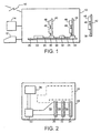
- FIG. 1 is a schematic cross-section of a computer system 10, which comprises of a backplane, or motherboard, or main board 20.
- a backplane or motherboard, or main board 20.
- FIG. 1 is a schematic cross-section of a computer system 10, which comprises of a backplane, or motherboard, or main board 20.
- a backplane it should be understood that the reference to a backplane is intended to relate to a board or other carrier plane on which at least one bus is provided, and to which at least one expansion, or additional card can be connected via a connector, or socket.
- a bus controller 22 is represented schematically on the backplane 20.
- the bus controller 22 is connected via a bus 24 to a plurality of sockets, or connectors, 30, 32 and 34.
- Each of the connectors 30, 32 and 34 is provided with a plurality of contacts for making contact with corresponding contacts on an insertable card.
- two cards 40 and 44 are shown inserted in the connectors 30 and 34, respectively.
- the individual cards 40 and 44 are provided with electronic circuits and or other components 46 which are connected by printed circuit or other wiring 48 to connectors provided at one edge of the card, either directly at the edge on the card or by means of a separate connector (not shown).
- the connector 32 is not populated in Figure 1.
- a further card, 42 could also be inserted in the connector 32 to expand the computer system 10.
- Figure 1 also illustrates the card 42 provided with circuits 46, connected by printed circuit wiring 48 to an edge connector 38.
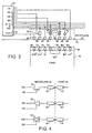
- Figure 2 is a schematic plan view of the backplane 20 illustrated in side view in Figure 1.
- Figure 2 is a schematic diagram showing only those components relevant to the description of the present invention.
- Figure 2 schematically shows a processor 26 connected to the bus controller 22 and schematically shows additional circuitry 28.
- the computer system 10 can include any normal configuration of a computer system with additional circuitry including timing circuitry, control circuitry, data storage devices, etc.
- data entry and output devices such as a keyboard 12 and display 14 can form part of the computer system 10, as can a connection to a network 16, etc.
- Some of the connections to external devices such as a display 14, or an external network, can be provided by means of the circuitry on one of the insertable cards, or alternatively such interfaces can be provided from the backplane circuitry 28 in a manner which will be immediately apparent to one skilled in the art.
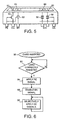
- the bus 24 shown schematically in Figures 1 and 2 comprises many different signal lines. Some of the signal lines of a bus in accordance with the present invention are shown in Figure 3. Some of the bus signal lines for connection to the insertable cards are required permanently. Such signals include, for example, power and clock signals and output signals such as a bus request signal which needs to be observed permanently. Other signals only need to be observed when a card carries out a data transaction during an appropriate bus cycle, for example data bus signals. An embodiment of the present invention can take account of this.
- FIG 3 a number of contacts 50, 54, 56, 60 and 64 in a connector 32 are illustrated schematically. These are for connection to respective contacts on a card 42.
- Figure 4 illustrates in more detail selected ones of the contacts shown in Figure 3.
- contact 50 in the connector 40 on the backplane 20 is connected to a bus line Vcc for supplying a power supply to the power supply contact 70 of an inserted card 42.
- the connector 40 or the backplane 20 is provided with a switch gate 52 (which is preferably configured as a field effect transistor) which is switched in response to a power enable PE signal also supplied over the backplane 20 from the bus controller 22.
- a contact 60 receives a bus request signal BR from a corresponding contact 80 of an inserted card 42.
- the bus request contact 60 is connected to a bus request line BR to the bus controller 22 via a bus request gate 62 which, as shown in Figure 4, can be made to be responsive to the power enable signal PE.
- the bus request gate 62 can be arranged to provide a delay after receipt of the power enable signal before enabling bus request signals to be passed from the contact 60 to the bus request line BR. The delay is set in order to give sufficient time for the circuitry on the card 42 to stabilise.
- the power enable signal PE is supplied for switching the switch 52 and for enabling the delay period to be commenced when it is detected, or the user signals, that the card 42 has been correctly inserted within the connector 32.
- bus request gate 62 it may be preferable to implement the bus request gate 62 as a simple gate operated under software control.
- a plurality of connectors 56 for data and address lines are provided.
- Each of the data/address contacts 56 is connected to a corresponding data/address line D/A on the backplane bus via a respective transmission gate 54.
- the transmission gates 58 are enabled by a gate enable signal GE, provided from the bus controller 22.
- FIG. 3 Also shown in Figure 3 is a ground contact 54 connected to a grounding line and a card enable contact 64 connected to a card enable line CE from the bus controller 22.
- Corresponding contacts 54 and 84 are provided on the card 42. It will be appreciated that additional contacts can be provided on the connector 32 and on the card 42 for additional signal lines as required by any particular implementation.
- Each of the contacts 70, 74, 76, 80 and 84 on the card 42 are connected to printed circuit or other wiring Vcc, G, D/A, BR, CE on the card 42 for connection to the appropriate functional units on that card.
- the data/address lines D/A are provided in parallel to each of the connectors 30, 32 and 34.
- the power and ground lines Vcc and G are provided in parallel to the connectors 30, 32 and 34.
- Separate bus requests, gate enable, power enable and card enable lines are provided to each of the respective connectors 30, 32 and 34.
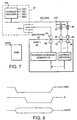
- FIG. 5 is a schematic representation of a connector for use on a backplane, which connector includes the various gates described with reference to Figure 4.
- a switch gate 52 here a FET
- the control signal PE is supplied via a PE pin.
- the PE signal is also supplied to a delay circuit 62 which is provided between a contact 60 and a pin BR.
- a plurality of transmission gates 58 are provided in line between data/address contact 60 and D/A pins.
- the control input for each transmission gate 58 is connected to a GE pin. It will be appreciated that Figure 5 is merely schematic and only illustrates selected pins. In practice, many more pins would be provided, and the connector may take on any standard or alternative connector configurations.
- the switch 52 and the transmission gates 58 would be provided in the connector, in alternative embodiments, other configurations of gates could be provided within the connector, subject to there being at least selected gates connected between critical contacts of the connector and corresponding pins for connection to printed circuit or other wiring on the backplane.
- Figure 6 is a flow diagram for schematically illustrating the selective enabling of the various contacts in the connector 32 when the card 42 is inserted.
- the process is initiated by the user inserting the edge connector 38 of the card 42 into the connector 32 on the backplane 20.
- a mechanism is provided 92 for detecting correct insertion of the card. This could be performed by the user inputting appropriate data into the computer 10 to confirm that the card has been correctly inserted.
- automatic means could be provided for detecting the correct insertion of the card. Optionally, this could be by sensing a particular signal level at a contact 66, which on insertion of the card 42 makes contact with the further contact 86 on the card, over a line (e.g. an acknowledge line ACK) to the controller 22.
- a mechanical sensor could be provided to detect the correct insertion of the card connector 38 in the backplane connector 32.
- impedance values on an existing line could be used to detect correct insertion of the card.
- a power supply signal PE is supplied at 94 from the bus controller 22 to the switch 54 for enabling power 50 to be supplied to the card 42. This ensures that power is not supplied until all the appropriate connections have been made.
- the power enable PE signal is also supplied to the delay stage 62 to prevent bus request signals being received by the bus controller 22 from the insert card 42 until circuitry on that card has stabilised. This ensures that spurious bus request signals and/or other spikes are not sent to the bus controller 22.
- the card When the bus request signal line has been enabled in step 96, the card is then fully operational and the power supply, clock and other permanently required signals are available permanently to the card 42. Also, the bus request line from the card is permanently monitored.
- the data/address contacts 56 of the connector 32 are only enabled at appropriate bus cycle times for the card 42 in question, thus providing dynamic cycle switching.
- two mechanisms are employed by the bus controller 22 for determining when the data/address contacts 56 are enabled for a particular card 42.
- the first mechanism is to enable the data/address contacts 56 by supplying a gate enable signal to the appropriate transmissions gates 58 when the card 42 in question when the controller grants the bus to the card in response to the card asserting the bus request line for that card. It will be noted that there is one bus request line on the backplane 20 for each card connector 30, 32, 34 etc. Accordingly, the bus controller 22 knows immediately which card has asserted respective bus request lines, enables the appropriate transmission gates 58 by supplying an appropriate gate enable signal to the card in question at the same time as granting bus access during the appropriate bus cycle.
- FIG. 7 An alternative mechanism as represented in Figure 7 is employed when the card in question is operating in the slave mode under the control of the controller 22.
- the card controller 22 employs geographic addressing to address the individual cards. This achieved by employing programmable addressing (for example as provided in accordance with the PCI standard).
- programmable addressing for example as provided in accordance with the PCI standard.
- the bus controller 22 is provided with an address decoder 100 which is responsive to an address on address lines 102 to generate the gate enable signals GE0-GE3 for (in this case) up to four separate cards (it will be remembered that only three card connectors are shown and therefore only three card enable signals are needed, by way of example, in Figure 1).
- the bus controller 22 can thereby determine in advance the source of a response (acknowledgement ACK) to any cycle before the bus cycle commences, thereby enabling ready identification of a faulty card.
- the power enable signals and also the card enable signals are preferably provided under software control.
- Figure 3 illustrates a particular configuration of lines in Figure 3, it will be appreciated that this is merely one example of a possible line configuration for the backplane bus and the connectors 32/38. Alternative detailed configuration of bus lines can be provided. Also, it is possible for example, to provide the gate enable signals without the provision of separate gate enable lines on the backplane bus.
- Figure 8 illustrates the use of a radial address line, RAD, which would be provided separately for each of the individual connectors 32 and a common strobe to determine the timing of the opening of the transmission gates 58.
- the strobe signal is supplied in common to all the cards, this could be used in combination with the selectively addressed RAD signal to ensure that the transmission gates for a particular card are enabled during the appropriate cycle for that card.
- An embodiment of the invention can isolate each connector of a bus (for example PCI bus) by the placing of transmission gates (for example configured as field effect transistors) on the backplane between PCI bus connectors.
- the transmission gates can be provided as an integral component in a connector for the insertion of a backplane card or could be provided on the backplane bus itself.
- An embodiment of the invention can enable rapid and reliable fault detection through the use of geographical decoding of the bus addresses whereby the bus controller will know immediately which connector (slot) has a bus connected to it in which a fault has occurred as the bus controller will know in advance which card will respond to any cycle before that cycle issues.
- the overall effective transmission line over the backplane bus is reduced to the line length on the backplane plus the transmission line length on the selected card. This provides significant transmission line advantages enabling reduced electromagnetic interference, and reliable higher frequency operation.
- fault isolation becomes much easier as a fault, for example a short on a bus line bit, will only manifest itself when the transmission gates for the faulty card are enabled. It will be appreciated that fault isolation is therefore facilitated.
- the additional backplane transistor isolation provided for power supply lines, clocks, etc are a preferred embodiment of the invention, which are enabled when the card is turned on and are kept enabled until it is turned off. In a preferred embodiment of the invention as described herein, a number of advantages are provided.
Description
- This invention relates to managing an expandable computer bus architecture.
- Open system architectures are well known in computer systems. Open computer system architectures are based on the provision of a computer bus which can be expanded by means of expansion cards. In order to provide for computer bus expansion, on a typical backplane, or motherboard, a computer bus will be provided with a number of sockets into which expansion cards can be inserted. There are a number of different standards for computer bus expansions. One conventional standard is the PCI (Peripheral Component Interface) architecture. The PCI architecture enables a bus to be expanded by the insertion of cards, but the standard PCI architecture is less than ideal for a highly reliable system for a number of reasons. Firstly, PCI cards are not hot replaceable, meaning that the cards cannot be inserted when the system is actually running. Accordingly, it is necessary to turn off the main computer system in order to carry out maintenance and insert new cards. Also, it is difficult to tell exactly which card might be generating a fault which can be identified on the bus. Accordingly, this increases maintenance and repairs costs where a fault develops. A further difficulty of PCI cards is the limitation placed on the size of the system which can be produced due to the bus trace length limit for signal propagation. This is a particular problem if easy maintenance is to be enabled. Reliable and easily maintained systems may demand a configuration of bus paths which results in particularly long signal paths. This limits the physical size of the system which can be manufactured due to transmission line factors.
- European patent application EP-A-0,632,393 describes an apparatus and a method of connecting an IC card to a motherboard. On detecting that an IC card has been inserted into a connector located on the motherboard, a power bus of and a general signal bus of the motherboard are connected to a power bus and a general signal bus of the IC card, respectively. A connector circuit located on the motherboard between the motherboard power bus and the connector and between the motherboard general signal bus and the connector controls the making of the connections. European patent application EP-A-0,811,932 and International application WO 93/15459 also describe similar switch circuitry on a motherboard for selectively connecting bus lines on the motherboard to a connector for receiving a circuit card.
- It is an aim of the present invention to address at least some of the above identified problems of conventional bus systems.
- Aspects of the invention are defined in the accompanying claims.
- One aspect of the invention provides multi-contact connector for the connection of an expansion card to a computer backplane, said connector comprising a gate electrically connected in-line between a line connector pin for connection to a line on a said backplane and a line contact for connection to a corresponding line contact on an inserted expansion card, a gate signal input of said gate being electrically connected to a gate signal connector pin for connection to a gate signal line on a said backplane
- The provision of a gate in the connector between the bus line and the connector contact enables control of the input/output to a card inserted or to be inserted in the connector.
- Thus, the contact can be enabled selectively, for example continuously from some predetermined time or for a particular bus cycle. This control provides a basis for enabling hot insertion and removal of a card for a running system, in that the appropriate contacts can be disabled, preventing bus errors and card malfunctions. Also, where a PCI bus controller on the backplane is to be provided, standard cold-insertable PCI cards can be used.
- A plurality of transmission gates (for example implemented by a pair of FETs) can be provided, each electrically connected in-line between a respective connector pin for connection to a line on a backplane and a respective contact for connection to a corresponding contact on an inserted expansion card. Respective gate signal inputs for each of transmission gates are electrically connected to a common connector pin for connection to a gate signal line.
- The connector can also comprise a switch gate (for example implemented by an FET) electrically connected in-line between a connector pin for connection to a power line on a backplane and a contact for connection to a corresponding power contact on an inserted expansion card, a control input of the switch gate being electrically connected to a connector pin for connection to a power signal line.
- Another aspect of the invention provides a backplane for a computer system, the backplane having mounted thereon at least one such multi-contact connector for expansion cards, at least one bus line for connection to a predetermined line contact of said connector(s) and a gate signal line for supplying a gate signal to said gate signal connector pin.
- A respective gate signal line can be provided for each of a plurality of connectors, whereby selective control of the gates for respective connectors can be provided. This further enables dynamic cycle switching of the cards to be achieved.
- The bus can comprise a plurality of data lines for connection to respective data contacts of a connector, a respective transmission gate (preferably implemented by a pair of FETs - field effect transistors) being provided between each data line and the respective contact of the connector, thereby enabling selective gating of the data and address signals to and from a connected card. For a multi-connector system, a respective gate signal line can be provided for each of a plurality of connectors, with the gate signal being supplied in parallel to each transmission gate of a connector. Alternatively, a plurality of gate signal lines can be provided for a connector so that individual transmission gates can be enabled at timings selected for the lines concerned.
- At least one power line can be provided for connection to a power contact of the connector(s), a switch gate (preferably implemented by an FET) being connected between the power line and the power contact of a connector and a power signal line for supplying a power control signal to control the switch gate. This enables the selective application of power to the card following correct insertion of the card.
- Also, at least one bus request line can be connected to a bus request contact of a connector and a bus request gate for selectively passing the bus request signal from the bus request connector to the bus request line. The bus request gate can be operable in use to pass a bus request signal only after a predetermined delay following power being supplied to a card connected to the connector. In this way, it is possible to allow for the circuits of card to settle after application of power to the card, avoiding transients and other false signals from disrupting the operation of a computer system incorporating the backplane.
- The gate signal line can be implemented using a strobe line common to each connector, the strobe line being active, in use, as the gate line when a radial address signal on a radial address signal line for the connector is active.
- A further aspect of the invention provides a computer system comprising such a backplane and a bus controller connected to said bus line for data transmission and connected to said gate signal line for supplying a gate signal for said gate.
- The bus controller can selectively supply a gate signal in parallel to each transmission gate of only one connector for a given bus cycle for enabling the transmissions gates of the connector for the given bus cycle, whereby dynamic cycle switching can be provided.
- The bus controller can selectively apply a power control signal on the power control signal line when a card has been inserted in the connector.
- The bus controller can comprise an address decoder providing geographic decoding of address signals for respective cards, whereby the bus controller can determine in advance the source of a response to any bus cycle before the bus cycle commences.
- Where the bus is a PCI bus, the provision of geographic addressing enables conventional PCI cards to be used with the significant advantage that isolation of faults in a particular PCI card is facilitated. Indeed, an embodiment of the invention can provide a method of configuring a PCI bus mechanism to provide geographic addressing of cards connected to the bus, whereby the bus controller can determine in advance the source of a response to any bus cycle before the bus cycle commences. Geographic addressing in a PCI context overcomes the difficulty of prior PCI implementations in which the isolation of faults on a PCI bus is difficult and time consuming. As the bus controller can determine in advance the source of a response to any bus cycle before the bus cycle commences, the location of a faulty card can be readily identified.
- Another aspect of the invention provides a method of connecting an expansion card to a backplane of a computer system, said method comprising steps of: inserting an expansion card into a multi-contact connector as described above for said expansion card; and subsequently enabling said gate by supplying a gate signal on a gate signal line to said gate. The method can include the hot-insertion of the card into the multi-contact connector.
- To facilitate fault isolation and to reduce transmission line problems, the bus controller preferably supplies a gate signal for enabling the transmission gates of only one connector for a given bus cycle.
- The method can include a further step between the insertion step and the enabling step of: supplying a power supply signal to a power switch connected between a power line and a power contact of the connector when the card has been inserted in the connector, whereby power is supplied to the card only after insertion, thereby providing dynamic cycle switching.
- The method can also include a further step after the step of supplying a power signal of: enabling a bus request signal to be passed from a bus request contact of the connector only after a predetermined delay following the supply of power to the card. These further steps facilitate the insertion of the card when the computer is system is live.
- A method of an embodiment of the invention employs geographic addressing by a bus controller to cards connected to the computer system, whereby the bus controller can determine in advance the source of a response to any bus cycle before the bus cycle commences.
- Exemplary embodiments of the present invention will be described hereinafter with reference to the accompanying drawings in which like reference signs are applied to like elements and in which;
- Figure 1 is a schematic cross section of a computer system showing a backplane and a number of expansion cards;
- Figure 2 is a schematic plan view of the backplane of Figure 1;
- Figure 3 is a schematic diagram illustrating some of the connections from a bus controller to an insertable card;
- Figure 4 illustrates in more detail some of the elements of Figure 3;
- Figure 5 is a schematic representation of a connector for an expansion card;
- Figure 6 is a flow diagram illustration hot insertion of a card;
- Figure 7 is a schematic diagram illustrating aspects of geographical addressing;
- Figure 8 represents one possible technique for providing signal in one embodiment of the invention.
-
- Figure 1 is a schematic cross-section of a
computer system 10, which comprises of a backplane, or motherboard, ormain board 20. Although reference is made hereinafter to a "backplane", it should be understood that the reference to a backplane is intended to relate to a board or other carrier plane on which at least one bus is provided, and to which at least one expansion, or additional card can be connected via a connector, or socket. - In Figure 1, a
bus controller 22 is represented schematically on thebackplane 20. Thebus controller 22 is connected via abus 24 to a plurality of sockets, or connectors, 30, 32 and 34. Each of theconnectors cards connectors individual cards other components 46 which are connected by printed circuit orother wiring 48 to connectors provided at one edge of the card, either directly at the edge on the card or by means of a separate connector (not shown). It will be noted that theconnector 32 is not populated in Figure 1. A further card, 42 could also be inserted in theconnector 32 to expand thecomputer system 10. Figure 1 also illustrates thecard 42 provided withcircuits 46, connected by printedcircuit wiring 48 to anedge connector 38. - In order to avoid having to turn off the
computer system 10 in order to be able to insert thecard 42, it would be desirable to be able to hot insert thecard 42. In accordance with an embodiment of the present invention, this would be possible as will be described hereinafter. - Figure 2 is a schematic plan view of the
backplane 20 illustrated in side view in Figure 1. Figure 2 is a schematic diagram showing only those components relevant to the description of the present invention. In addition to the components shown in Figure 1, and identified by like reference numerals, Figure 2 schematically shows aprocessor 26 connected to thebus controller 22 and schematically showsadditional circuitry 28. - It will be appreciated that the
computer system 10 can include any normal configuration of a computer system with additional circuitry including timing circuitry, control circuitry, data storage devices, etc. Also, as shown schematically in Figure 1, data entry and output devices such as akeyboard 12 anddisplay 14 can form part of thecomputer system 10, as can a connection to anetwork 16, etc. Some of the connections to external devices such as adisplay 14, or an external network, can be provided by means of the circuitry on one of the insertable cards, or alternatively such interfaces can be provided from thebackplane circuitry 28 in a manner which will be immediately apparent to one skilled in the art. - The
bus 24 shown schematically in Figures 1 and 2 comprises many different signal lines. Some of the signal lines of a bus in accordance with the present invention are shown in Figure 3. Some of the bus signal lines for connection to the insertable cards are required permanently. Such signals include, for example, power and clock signals and output signals such as a bus request signal which needs to be observed permanently. Other signals only need to be observed when a card carries out a data transaction during an appropriate bus cycle, for example data bus signals. An embodiment of the present invention can take account of this. - In Figure 3, a number of
contacts connector 32 are illustrated schematically. These are for connection to respective contacts on acard 42. Figure 4 illustrates in more detail selected ones of the contacts shown in Figure 3. - In particular,
contact 50 in theconnector 40 on thebackplane 20 is connected to a bus line Vcc for supplying a power supply to thepower supply contact 70 of an insertedcard 42. However, rather than thecontact 50 being connected directly to the power supply line Vcc, theconnector 40 or thebackplane 20 is provided with a switch gate 52 (which is preferably configured as a field effect transistor) which is switched in response to a power enable PE signal also supplied over thebackplane 20 from thebus controller 22. - A
contact 60 receives a bus request signal BR from acorresponding contact 80 of an insertedcard 42. Thebus request contact 60 is connected to a bus request line BR to thebus controller 22 via abus request gate 62 which, as shown in Figure 4, can be made to be responsive to the power enable signal PE. In this case, thebus request gate 62 can be arranged to provide a delay after receipt of the power enable signal before enabling bus request signals to be passed from thecontact 60 to the bus request line BR. The delay is set in order to give sufficient time for the circuitry on thecard 42 to stabilise. - The power enable signal PE is supplied for switching the
switch 52 and for enabling the delay period to be commenced when it is detected, or the user signals, that thecard 42 has been correctly inserted within theconnector 32. - Alternatively, and particularly where a greater degree of flexibility is required, it may be preferable to implement the
bus request gate 62 as a simple gate operated under software control. - A plurality of
connectors 56 for data and address lines are provided. Each of the data/address contacts 56 is connected to a corresponding data/address line D/A on the backplane bus via arespective transmission gate 54. Thetransmission gates 58 are enabled by a gate enable signal GE, provided from thebus controller 22. - Also shown in Figure 3 is a
ground contact 54 connected to a grounding line and a card enablecontact 64 connected to a card enable line CE from thebus controller 22.Corresponding contacts 54 and 84 are provided on thecard 42. It will be appreciated that additional contacts can be provided on theconnector 32 and on thecard 42 for additional signal lines as required by any particular implementation. - Each of the
contacts card 42 are connected to printed circuit or other wiring Vcc, G, D/A, BR, CE on thecard 42 for connection to the appropriate functional units on that card. - As represented in Figure 3, the data/address lines D/A are provided in parallel to each of the
connectors connectors respective connectors - Figure 5 is a schematic representation of a connector for use on a backplane, which connector includes the various gates described with reference to Figure 4. A switch gate 52 (here a FET) is connected between a Vcc pin and the
contact 50. The control signal PE is supplied via a PE pin. The PE signal is also supplied to adelay circuit 62 which is provided between acontact 60 and a pin BR. Also, a plurality oftransmission gates 58 are provided in line between data/address contact 60 and D/A pins. The control input for eachtransmission gate 58 is connected to a GE pin. It will be appreciated that Figure 5 is merely schematic and only illustrates selected pins. In practice, many more pins would be provided, and the connector may take on any standard or alternative connector configurations. - Although, in a preferred embodiment, at least the
switch 52 and thetransmission gates 58 would be provided in the connector, in alternative embodiments, other configurations of gates could be provided within the connector, subject to there being at least selected gates connected between critical contacts of the connector and corresponding pins for connection to printed circuit or other wiring on the backplane. - Figure 6 is a flow diagram for schematically illustrating the selective enabling of the various contacts in the
connector 32 when thecard 42 is inserted. - The process is initiated by the user inserting the
edge connector 38 of thecard 42 into theconnector 32 on thebackplane 20. A mechanism is provided 92 for detecting correct insertion of the card. This could be performed by the user inputting appropriate data into thecomputer 10 to confirm that the card has been correctly inserted. Alternatively, automatic means could be provided for detecting the correct insertion of the card. Optionally, this could be by sensing a particular signal level at acontact 66, which on insertion of thecard 42 makes contact with thefurther contact 86 on the card, over a line (e.g. an acknowledge line ACK) to thecontroller 22. As a further alternative, a mechanical sensor could be provided to detect the correct insertion of thecard connector 38 in thebackplane connector 32. As a further alternative, impedance values on an existing line could be used to detect correct insertion of the card. - Irrespective of the particular method used to detect correct insertion of the card, when this is detected at
step 92, a power supply signal PE, is supplied at 94 from thebus controller 22 to theswitch 54 for enablingpower 50 to be supplied to thecard 42. This ensures that power is not supplied until all the appropriate connections have been made. - As illustrated in Figure 4, the power enable PE signal is also supplied to the
delay stage 62 to prevent bus request signals being received by thebus controller 22 from theinsert card 42 until circuitry on that card has stabilised. This ensures that spurious bus request signals and/or other spikes are not sent to thebus controller 22. - When the bus request signal line has been enabled in
step 96, the card is then fully operational and the power supply, clock and other permanently required signals are available permanently to thecard 42. Also, the bus request line from the card is permanently monitored. - However, in preferred embodiment of the present invention, the data/
address contacts 56 of theconnector 32 are only enabled at appropriate bus cycle times for thecard 42 in question, thus providing dynamic cycle switching. - In the preferred embodiment of the invention, two mechanisms are employed by the
bus controller 22 for determining when the data/address contacts 56 are enabled for aparticular card 42. - The first mechanism is to enable the data/
address contacts 56 by supplying a gate enable signal to theappropriate transmissions gates 58 when thecard 42 in question when the controller grants the bus to the card in response to the card asserting the bus request line for that card. It will be noted that there is one bus request line on thebackplane 20 for eachcard connector bus controller 22 knows immediately which card has asserted respective bus request lines, enables theappropriate transmission gates 58 by supplying an appropriate gate enable signal to the card in question at the same time as granting bus access during the appropriate bus cycle. - An alternative mechanism as represented in Figure 7 is employed when the card in question is operating in the slave mode under the control of the
controller 22. In order that the controller can predict which card is addressed in such a mode, thecard controller 22 employs geographic addressing to address the individual cards. This achieved by employing programmable addressing (for example as provided in accordance with the PCI standard). Thus software effectively allocates a block of address space to a card (e.g. card 1) as represented schematically in Figure 7, for example, by a 256K block having a base address BASE. Accordingly, as schematically represented in Figure 7, thebus controller 22 is provided with anaddress decoder 100 which is responsive to an address onaddress lines 102 to generate the gate enable signals GE0-GE3 for (in this case) up to four separate cards (it will be remembered that only three card connectors are shown and therefore only three card enable signals are needed, by way of example, in Figure 1). Thebus controller 22 can thereby determine in advance the source of a response (acknowledgement ACK) to any cycle before the bus cycle commences, thereby enabling ready identification of a faulty card. The power enable signals and also the card enable signals are preferably provided under software control. - Although a particular configuration of lines is shown in Figure 3, it will be appreciated that this is merely one example of a possible line configuration for the backplane bus and the
connectors 32/38. Alternative detailed configuration of bus lines can be provided. Also, it is possible for example, to provide the gate enable signals without the provision of separate gate enable lines on the backplane bus. For example, Figure 8 illustrates the use of a radial address line, RAD, which would be provided separately for each of theindividual connectors 32 and a common strobe to determine the timing of the opening of thetransmission gates 58. Firstly, although the strobe signal is supplied in common to all the cards, this could be used in combination with the selectively addressed RAD signal to ensure that the transmission gates for a particular card are enabled during the appropriate cycle for that card. - There has been described a bus configuration which can enable hot insertion, fault isolation, and bus expansion for a standard backplane bus by the provision of transmission gates.
- An embodiment of the invention can isolate each connector of a bus (for example PCI bus) by the placing of transmission gates (for example configured as field effect transistors) on the backplane between PCI bus connectors. The transmission gates can be provided as an integral component in a connector for the insertion of a backplane card or could be provided on the backplane bus itself.
- An embodiment of the invention can enable rapid and reliable fault detection through the use of geographical decoding of the bus addresses whereby the bus controller will know immediately which connector (slot) has a bus connected to it in which a fault has occurred as the bus controller will know in advance which card will respond to any cycle before that cycle issues.
- By enabling the transmission gates for only the targeted connector in any bus cycle, the overall effective transmission line over the backplane bus is reduced to the line length on the backplane plus the transmission line length on the selected card. This provides significant transmission line advantages enabling reduced electromagnetic interference, and reliable higher frequency operation.
- Also, fault isolation becomes much easier as a fault, for example a short on a bus line bit, will only manifest itself when the transmission gates for the faulty card are enabled. It will be appreciated that fault isolation is therefore facilitated.
- The additional backplane transistor isolation provided for power supply lines, clocks, etc are a preferred embodiment of the invention, which are enabled when the card is turned on and are kept enabled until it is turned off. In a preferred embodiment of the invention as described herein, a number of advantages are provided.
- A) A card is hot insertable as a result of keeping all of the gates turned off while inserting or removing the card.
- B) No leading pin connector is required on a card to enable hot insertion as any signal can touch first with the gates turned off.
- C) Features A and B together mean that a standard cold insertable PCI card can be used in a hot maintained system.
- D) Transmission lines are much shorter as only one PCI slot is enabled at any one time - each individual PCI slot can have quite long bus traces which are isolated by the gates and do not effect the overall system, enabling PCI bus physical lengths which can rise from the usual 0.7 meters limit to about 2 meters, making additional physical system configuration.
- E) Where the bus talks to only one slot at a time, faults in that slot cannot effect other slots. Thus a PCI card in an embodiment of the invention can short all other PCI bus lines to ground and yet the other slots will still work perfectly. This enables good fault isolation of a single replaceable module.
-
- Although particular embodiments of the inventions have been described, it will be appreciated that the invention is not limited thereto, and many modifications and/or additions may be made within the scope of the invention.
Claims (31)
- A multi-contact connector (32) for the connection of an expansion card (42) to a computer backplane (20), said connector comprising a gate (58) electrically connected in-line between a line connector pin (D/A) for connection to a line on said computer backplane and a line contact (56) for connection to a corresponding line contact (76) on an inserted expansion card, a gate signal input of said gate being electrically connected to a gate signal connector pin (GE) for connection to a gate signal line on said computer backplane.
- A connector according to Claim 1, comprising a plurality of said gates, each electrically connected in-line between a respective line connector pin and a respective line contact for connection to a corresponding line contact on an inserted expansion card.
- A connector according to Claim 2, wherein respective gate signal inputs for each of said gates are electrically connected to a common gate signal connector pin for connection to a gate signal line.
- A connector according to Claim 2, wherein respective gate signal inputs for each of said gates are electrically connected to separate gate signal connector pins for connection to respective gate signal lines.
- A connector according to any one of Claims 1 to 4, additionally comprising a switch (52) electrically connected in-line between a power line connector pin (Vcc) for connection to a power line on a said backplane and a power line contact (50) for connection to a corresponding power line contact (70) on an inserted expansion card, a control input of said switch gate being electrically connected to a control signal connector pin (PE) for connection to a power control signal line.
- A connector according to any one of Claims 1 to 5, additionally comprising a bus request gate (62) electrically connected in-line between a bus request line contact (60) for connection to a corresponding bus request line contact (80) on an inserted expansion card and a bus request line connector pin (BR) for connection to a bus request line on a said backplane, said bus request gate being configured selectively to pass said bus request signal from said bus request contact to said bus request line.
- A backplane for a computer system, the backplane having mounted thereon at least one multi-contact connector according to any preceding claim for expansion cards, at least one bus line for connection to a predetermined line contact of said connector(s) and a gate signal line for supplying a gate signal to said gate signal connector pin.
- A backplane according to Claim 7, wherein at least a respective gate signal line is provided for each of a plurality of connectors to enable dynamic cycle switching.
- A backplane according to Claim 8, wherein said bus comprises at least a plurality of data lines (D/A) for connection to respective data line contacts (56) of a said connector, a respective said gate forming a transmission gate (58) being provided between each said data line and the respective data line contact of said connector.
- A backplane according to Claim 9, wherein a respective gate signal line (GE) is provided for each of a plurality of connectors, said gate signal being supplied in parallel to each transmission gate of a said connector.
- A backplane according to Claim 9, wherein a plurality of gate signal lines (GE) are provided for each connector, whereby transmission gates of different data line contacts of a connector may be gated independently.
- A backplane according to any one of Claims 9 to 11, comprising at least one power line (Vcc) for connection to a power contact (50) of said connector(s), a switch gate in said connector being connected between said power line and the power contact of a said connector and a power signal line (PE) for supplying a power control signal to control said switch gate.
- A backplane according to any one of Claims 9 to 12, comprising at least one bus request line (BR) connected to a bus request contact (60) of a said connector, a bus request gate (62) in said connector being operable selectively to pass said bus request signal from said bus request connector to said bus request line.
- A backplane according to Claim 13, wherein said bus request gate is operable in use to pass a bus request signal only after a predetermined delay following power being supplied to a card connected to said connector.
- A backplane according to any of Claims 7 to 14, wherein said gate signal line is a strobe line common to each connector, said strobe line being active, in use, as said gate line when a radial address signal on a radial address signal line for said connector is active.
- A computer system comprising a backplane according to any one of Claims 7 to 15, and a bus controller connected to said bus line for data transmission and connected to said gate signal line for supplying a gate signal for said gate.
- A system according to Claim 16, wherein a respective gate signal line is provided for each of a plurality of connectors, said bus controller selectively supplying a gate signal for enabling transmission gates of one said connector for a given bus cycle to provide dynamic cycle switching.
- A system according to Claim 16 or Claim 17, wherein said bus comprises at least a plurality of data lines for connection to respective data line contacts of a said connector, a respective transmission gate being provided between each said data line and the corresponding data line contact of said connector.
- A system according to Claim 18, wherein a respective gate signal line is provided for each of a plurality of connectors, said bus controller selectively supplying a gate signal in parallel to each transmission gate of only one connector for a given bus cycle for enabling said transmission gates of said connector for said given bus cycle.
- A system according to Claim 18, wherein a plurality of respective gate signal lines is provided for each of a plurality of connectors, said bus controller selectively supplying gate signal at appropriate timings to each transmission gate of only one connector for a given bus cycle for enabling said transmission gates of said connector for said given bus cycle.
- A system according to any one of Claims 16 to 20, comprising at least one power line for connection to a power contact of said connector(s), a switch gate being connected between said power line and the power contact of a said connector, a power signal line for supplying a power control signal to control said switch gate of said connector, wherein said bus controller selectively applies a power control signal on said power control signal line when a card has been inserted in said connector.
- A system according to any one of Claims 16 to 21, wherein said gate signal line is a strobe line common to each connector, said strobe line being active, in use, as said gate line when a radial address signal on a radial address signal line for said connector is active.
- A system according to any one of Claims 16 to 22, wherein said bus controller comprises an address decoder providing geographic decoding of address signals for respective cards, whereby said bus controller can determine in advance the source of a response to any bus cycle before said bus cycle commences.
- A system according to Claim 23, comprising a PCI bus having geographic addressing of address signals.
- A method of connecting an expansion card to a backplane of a computer system, said method comprising steps of:inserting an expansion card into a multi-contact connector according to any one of claims 1 to 6 for said expansion card;subsequently enabling said gate by supplying a gate signal on a gate signal line to said gate.
- A method according to Claim 25, wherein said card is hot-inserted into said multi-contact connector.
- A method according to Claim 25 or Claim 26, wherein a bus controller selectively supplies a gate signal for enabling transmission gates of only one said connector for a given bus cycle, thereby providing dynamic cycle switching.
- A method according to Claim 27, comprising a further step between said insertion step and said enabling step of:supplying a power supply signal to a switch in said connector provided between a power line and a power contact of said connector when said card has been inserted in said connector, whereby power is supplied to said card only after insertion.
- A method according to Claim 28, comprising a further step after said step of supplying a power signal of:enabling a bus request signal to be passed from a bus request contact of said connector only after a predetermined delay following the supply of power to said card.
- A method according to any one of Claims 25 to 29, wherein said insertion step is formed when said computer system is live.
- A method according to any one of Claims 25 to 30, comprising a step of applying geographic addressing by a bus controller to cards connected to said computer system, whereby said bus controller can determine in advance the source of a response to any bus cycle before said bus cycle commences.
Applications Claiming Priority (2)
| Application Number | Priority Date | Filing Date | Title |
|---|---|---|---|
| US08/769,146 US5974489A (en) | 1996-12-18 | 1996-12-18 | Computer bus expansion |
| US769146 | 1996-12-18 |
Publications (3)
| Publication Number | Publication Date |
|---|---|
| EP0849684A2 EP0849684A2 (en) | 1998-06-24 |
| EP0849684A3 EP0849684A3 (en) | 1998-07-22 |
| EP0849684B1 true EP0849684B1 (en) | 2004-08-25 |
Family
ID=25084599
Family Applications (1)
| Application Number | Title | Priority Date | Filing Date |
|---|---|---|---|
| EP97310178A Expired - Lifetime EP0849684B1 (en) | 1996-12-18 | 1997-12-16 | Computer bus expansion |
Country Status (4)
| Country | Link |
|---|---|
| US (1) | US5974489A (en) |
| EP (1) | EP0849684B1 (en) |
| JP (1) | JP4201369B2 (en) |
| DE (1) | DE69730401D1 (en) |
Cited By (1)
| Publication number | Priority date | Publication date | Assignee | Title |
|---|---|---|---|---|
| CN107621859A (en) * | 2017-08-28 | 2018-01-23 | 郑州云海信息技术有限公司 | The method that server and optimization high speed connector are connected impedance discontinuity with server |
Families Citing this family (8)
| Publication number | Priority date | Publication date | Assignee | Title |
|---|---|---|---|---|
| US6658507B1 (en) * | 1998-08-31 | 2003-12-02 | Wistron Corporation | System and method for hot insertion of computer-related add-on cards |
| US7069047B2 (en) * | 2001-01-19 | 2006-06-27 | Raze Technologies, Inc. | System and method for on-line insertion of line replaceable units in wireless and wireline access systems |
| US20020124121A1 (en) * | 2001-03-05 | 2002-09-05 | Hsiang-Chan Chen | High-density system |
| US6501660B1 (en) * | 2001-06-22 | 2002-12-31 | Sun Microsystems, Inc. | Reliable card detection in a CPCI system |
| US20030046468A1 (en) * | 2001-08-30 | 2003-03-06 | Hsiang-Chan Chen | High-density system having a plurality of system units |
| US7840732B2 (en) | 2006-09-25 | 2010-11-23 | Honeywell International Inc. | Stacked card address assignment |
| JP2008219173A (en) * | 2007-02-28 | 2008-09-18 | Brother Ind Ltd | Multi-functional peripheral |
| US11372462B2 (en) * | 2020-03-24 | 2022-06-28 | Hitachi Energy Switzerland Ag | Protected power and data bus connection of peripheral device and host device |
Family Cites Families (14)
| Publication number | Priority date | Publication date | Assignee | Title |
|---|---|---|---|---|
| EP0266016A2 (en) * | 1986-10-28 | 1988-05-04 | Eip Microwave Incorporated | Automatic circuit board configuration |
| US5038320A (en) * | 1987-03-13 | 1991-08-06 | International Business Machines Corp. | Computer system with automatic initialization of pluggable option cards |
| US5274769A (en) * | 1988-08-29 | 1993-12-28 | Fujitsu Limited | System for transferring data between blocks |
| JP2644554B2 (en) * | 1988-11-15 | 1997-08-25 | 株式会社日立製作所 | Information processing system |
| US5202965A (en) * | 1988-12-09 | 1993-04-13 | Bull, S.A. | Electronic system with a plurality of removable units |
| US5058004A (en) * | 1990-01-19 | 1991-10-15 | Gonen Ravid | Computer gate control circuitry and apparatus to enable a single computer to simultaneously and selectively control a multiplicity of hard disk drives |
| US5134617A (en) * | 1990-03-30 | 1992-07-28 | At&T Bell Laboratories | Single wire plug-in circuit board status monitor |
| US5268592A (en) * | 1991-02-26 | 1993-12-07 | International Business Machines Corporation | Sequential connector |
| WO1993015459A1 (en) * | 1992-02-03 | 1993-08-05 | Micro Industries | Live insertion of computer modules |
| US5473499A (en) * | 1993-06-30 | 1995-12-05 | Harris Corporation | Hot pluggable motherboard bus connection method |
| US5586271A (en) * | 1994-09-27 | 1996-12-17 | Macrolink Inc. | In-line SCSI bus circuit for providing isolation and bi-directional communication between two portions of a SCSI bus |
| US5805903A (en) * | 1996-05-21 | 1998-09-08 | Compaq Computer Corporation | Protection of computer system against incorrect card insertion during start-up |
| JPH09319669A (en) * | 1996-05-30 | 1997-12-12 | Mitsubishi Electric Corp | Pc card system device |
| US6101322A (en) * | 1996-06-05 | 2000-08-08 | Compaq Computer Corporation | Removal and insertion of expansion cards in a computer system |
-
1996
- 1996-12-18 US US08/769,146 patent/US5974489A/en not_active Expired - Lifetime
-
1997
- 1997-12-16 EP EP97310178A patent/EP0849684B1/en not_active Expired - Lifetime
- 1997-12-16 DE DE69730401T patent/DE69730401D1/en not_active Expired - Lifetime
- 1997-12-17 JP JP34745097A patent/JP4201369B2/en not_active Expired - Lifetime
Cited By (1)
| Publication number | Priority date | Publication date | Assignee | Title |
|---|---|---|---|---|
| CN107621859A (en) * | 2017-08-28 | 2018-01-23 | 郑州云海信息技术有限公司 | The method that server and optimization high speed connector are connected impedance discontinuity with server |
Also Published As
| Publication number | Publication date |
|---|---|
| DE69730401D1 (en) | 2004-09-30 |
| EP0849684A3 (en) | 1998-07-22 |
| US5974489A (en) | 1999-10-26 |
| JP4201369B2 (en) | 2008-12-24 |
| EP0849684A2 (en) | 1998-06-24 |
| JPH10187283A (en) | 1998-07-14 |
Similar Documents
| Publication | Publication Date | Title |
|---|---|---|
| KR100240921B1 (en) | Secondary i/o bus with expanded slot capacity and hot plugging capability | |
| KR100244836B1 (en) | Error recovery by isolation of peripheral components in a data processing system | |
| US7447822B2 (en) | Hot-plug control system and method | |
| EP0974085B1 (en) | Method and system for enabling nondisruptive live insertion and removal of feature cards in a computer system | |
| US6178526B1 (en) | Testing memory modules with a PC motherboard attached to a memory-module handler by a solder-side adaptor board | |
| US5644470A (en) | Autodocking hardware for installing and/or removing adapter cards without opening the computer system cover | |
| US7356742B2 (en) | Method and apparatus for testing a memory device in quasi-operating conditions | |
| US6339831B1 (en) | Automatic detecting unit for diagnosing a connection and identifying an external device, information processing apparatus, and external device | |
| KR20030022780A (en) | System and method for testing signal interconnections using built-in self test | |
| US5918023A (en) | System design to support either Pentium Pro processors, Pentium II processors, and future processor without having to replace the system board | |
| JP2000056871A (en) | Ems enhancement circuit for usb system | |
| US5953243A (en) | Memory module identification | |
| EP0849684B1 (en) | Computer bus expansion | |
| KR19980022696A (en) | How to change the computer system with CPU and the hardware configuration inside it | |
| US6678776B2 (en) | System for a card proxy link architecture | |
| US6434653B1 (en) | Method and apparatus for disabling power-on in a system requiring add-in modules | |
| JP2002050435A (en) | Live line insertion.extraction detecting circuit, and live line insertion.extraction detecting method | |
| US20040158424A1 (en) | Apparatus and method for verification of system interconnect upon hot-plugging of electronic field replaceable units | |
| KR19980063473A (en) | Fast PCI with TTL-compatible signaling | |
| EP0849737B1 (en) | Improvements in or relating to electronic systems | |
| JP2003248796A (en) | Pc card detection device | |
| US7269672B2 (en) | Bus system design method, bus system, and device unit | |
| JPH11305890A (en) | Hot line inserting and pulling-out device | |
| CN117290172A (en) | High-speed bus verification board, system and method | |
| CN115705270A (en) | Hard disk in-place detection device and method |
Legal Events
| Date | Code | Title | Description |
|---|---|---|---|
| PUAI | Public reference made under article 153(3) epc to a published international application that has entered the european phase |
Free format text: ORIGINAL CODE: 0009012 |
|
| PUAL | Search report despatched |
Free format text: ORIGINAL CODE: 0009013 |
|
| AK | Designated contracting states |
Kind code of ref document: A2 Designated state(s): DE FR GB IT NL SE |
|
| AX | Request for extension of the european patent |
Free format text: AL;LT;LV;MK;RO;SI |
|
| AK | Designated contracting states |
Kind code of ref document: A3 Designated state(s): AT BE CH DE DK ES FI FR GB GR IE IT LI LU MC NL PT SE |
|
| AX | Request for extension of the european patent |
Free format text: AL;LT;LV;MK;RO;SI |
|
| 17P | Request for examination filed |
Effective date: 19990115 |
|
| AKX | Designation fees paid |
Free format text: DE FR GB IT NL SE |
|
| RBV | Designated contracting states (corrected) |
Designated state(s): DE FR GB IT NL SE |
|
| 17Q | First examination report despatched |
Effective date: 20020222 |
|
| RAP1 | Party data changed (applicant data changed or rights of an application transferred) |
Owner name: SUN MICROSYSTEMS, INC. |
|
| GRAP | Despatch of communication of intention to grant a patent |
Free format text: ORIGINAL CODE: EPIDOSNIGR1 |
|
| GRAS | Grant fee paid |
Free format text: ORIGINAL CODE: EPIDOSNIGR3 |
|
| GRAA | (expected) grant |
Free format text: ORIGINAL CODE: 0009210 |
|
| AK | Designated contracting states |
Kind code of ref document: B1 Designated state(s): DE FR GB IT NL SE |
|
| PG25 | Lapsed in a contracting state [announced via postgrant information from national office to epo] |
Ref country code: NL Free format text: LAPSE BECAUSE OF FAILURE TO SUBMIT A TRANSLATION OF THE DESCRIPTION OR TO PAY THE FEE WITHIN THE PRESCRIBED TIME-LIMIT Effective date: 20040825 Ref country code: IT Free format text: LAPSE BECAUSE OF FAILURE TO SUBMIT A TRANSLATION OF THE DESCRIPTION OR TO PAY THE FEE WITHIN THE PRESCRIBED TIME-LIMIT;WARNING: LAPSES OF ITALIAN PATENTS WITH EFFECTIVE DATE BEFORE 2007 MAY HAVE OCCURRED AT ANY TIME BEFORE 2007. THE CORRECT EFFECTIVE DATE MAY BE DIFFERENT FROM THE ONE RECORDED. Effective date: 20040825 Ref country code: FR Free format text: LAPSE BECAUSE OF FAILURE TO SUBMIT A TRANSLATION OF THE DESCRIPTION OR TO PAY THE FEE WITHIN THE PRESCRIBED TIME-LIMIT Effective date: 20040825 |
|
| REG | Reference to a national code |
Ref country code: GB Ref legal event code: FG4D |
|
| REF | Corresponds to: |
Ref document number: 69730401 Country of ref document: DE Date of ref document: 20040930 Kind code of ref document: P |
|
| PG25 | Lapsed in a contracting state [announced via postgrant information from national office to epo] |
Ref country code: SE Free format text: LAPSE BECAUSE OF FAILURE TO SUBMIT A TRANSLATION OF THE DESCRIPTION OR TO PAY THE FEE WITHIN THE PRESCRIBED TIME-LIMIT Effective date: 20041125 |
|
| PG25 | Lapsed in a contracting state [announced via postgrant information from national office to epo] |
Ref country code: DE Free format text: LAPSE BECAUSE OF FAILURE TO SUBMIT A TRANSLATION OF THE DESCRIPTION OR TO PAY THE FEE WITHIN THE PRESCRIBED TIME-LIMIT Effective date: 20041126 |
|
| NLV1 | Nl: lapsed or annulled due to failure to fulfill the requirements of art. 29p and 29m of the patents act | ||
| PLBE | No opposition filed within time limit |
Free format text: ORIGINAL CODE: 0009261 |
|
| STAA | Information on the status of an ep patent application or granted ep patent |
Free format text: STATUS: NO OPPOSITION FILED WITHIN TIME LIMIT |
|
| 26N | No opposition filed |
Effective date: 20050526 |
|
| EN | Fr: translation not filed | ||
| PGFP | Annual fee paid to national office [announced via postgrant information from national office to epo] |
Ref country code: GB Payment date: 20161214 Year of fee payment: 20 |
|
| REG | Reference to a national code |
Ref country code: GB Ref legal event code: PE20 Expiry date: 20171215 |
|
| PG25 | Lapsed in a contracting state [announced via postgrant information from national office to epo] |
Ref country code: GB Free format text: LAPSE BECAUSE OF EXPIRATION OF PROTECTION Effective date: 20171215 |