EP0847589B1 - Feldemissionsanzeigevorrichtung mit fokusierungelektroden beimder anode und verfahren zu deren herstellung - Google Patents
Feldemissionsanzeigevorrichtung mit fokusierungelektroden beimder anode und verfahren zu deren herstellung Download PDFInfo
- Publication number
- EP0847589B1 EP0847589B1 EP96927327A EP96927327A EP0847589B1 EP 0847589 B1 EP0847589 B1 EP 0847589B1 EP 96927327 A EP96927327 A EP 96927327A EP 96927327 A EP96927327 A EP 96927327A EP 0847589 B1 EP0847589 B1 EP 0847589B1
- Authority
- EP
- European Patent Office
- Prior art keywords
- emitters
- anode
- layer
- display device
- voltage
- Prior art date
- Legal status (The legal status is an assumption and is not a legal conclusion. Google has not performed a legal analysis and makes no representation as to the accuracy of the status listed.)
- Expired - Lifetime
Links
Images

Classifications
-
- H—ELECTRICITY
- H01—ELECTRIC ELEMENTS
- H01J—ELECTRIC DISCHARGE TUBES OR DISCHARGE LAMPS
- H01J31/00—Cathode ray tubes; Electron beam tubes
- H01J31/08—Cathode ray tubes; Electron beam tubes having a screen on or from which an image or pattern is formed, picked up, converted, or stored
- H01J31/10—Image or pattern display tubes, i.e. having electrical input and optical output; Flying-spot tubes for scanning purposes
- H01J31/12—Image or pattern display tubes, i.e. having electrical input and optical output; Flying-spot tubes for scanning purposes with luminescent screen
-
- H—ELECTRICITY
- H01—ELECTRIC ELEMENTS
- H01J—ELECTRIC DISCHARGE TUBES OR DISCHARGE LAMPS
- H01J29/00—Details of cathode-ray tubes or of electron-beam tubes of the types covered by group H01J31/00
- H01J29/02—Electrodes; Screens; Mounting, supporting, spacing or insulating thereof
- H01J29/08—Electrodes intimately associated with a screen on or from which an image or pattern is formed, picked-up, converted or stored, e.g. backing-plates for storage tubes or collecting secondary electrons
- H01J29/085—Anode plates, e.g. for screens of flat panel displays
Definitions
- the present invention relates in general to field emission display devices, and in particular to field emission display devices with focusing electrodes.
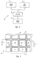
- a conventional field emission display device 10 includes a baseplate 12 having a plurality of field-induced electron emitters 14 carried by a supporting substrate 16. The emitters 14 are disposed within respective apertures in an insulating layer 18 deposited on the surface of the supporting substrate 16. Also, a conductive layer forming an extraction grid 20 is deposited on the insulating layer 18 peripherally about the respective apertures of the emitters 14.
- the conventional field emission display device 10 shown in Figure 1 also includes a faceplate 22 having a transparent viewing layer 24 separated from the baseplate 12 by spacers (not shown) between the faceplate 22 and the baseplate 12.
- An anode 26 such as an Indium tin oxide layer is deposited on a surface of the viewing layer 24 facing the baseplate 12.
- localized portions of a luminescent layer 28 are deposited on the anode 26.
- the luminescent layer 28 typically comprises a phosphorescent material, such as a cathodophosphorescent material, which emits light when bombarded by electrons.
- a black matrix 30 is deposited on the anode 26 between the localized portions of the luminescent layer 28 to improve the contrast of the field emission display device 10 by absorbing ambient light.
- a conductive voltage V c such as 40 volts applied to the extraction grid 20 and a source voltage V s such as 0 volts applied to the emitters 14 creates an intense electric field around the emitters 14. This electric field causes an electron emission to occur from each of the emitters 14 in accordance with the well-known Fowler-Nordheim equation.
- An anode voltage V a such as 1,000 volts applied to the anode 26 draws these electron emissions toward the faceplate 22. Some of these electron emissions impact on the localized portions of the luminescent layer 28 and cause the luminescent layer 28 to emit light. In this manner, the field emission display device 10 provides a display.
- field emission display device 10 is shown in Figure 1 having only two emitters 14 associated with each localized portion of the luminescent layer 28 for ease of understanding, those with skill in the field of this invention will understand that hundreds of emitters 14 may be associated with each localized portion of the luminescent layer 28 in order to average out individual differences in the electron emissions from different emitters 14.
- each localized portion of the luminescent layer of the display device comprises one pixel of the monochrome display.
- each localized portion of the luminescent layer comprises a green, red or blue sub-pixel of the color display, and a green, a red and a blue sub-pixel together comprise one pixel of the color display.
- the electron emission from an emitter associated with a first localized portion of the luminescent layer of a conventional field emission display device also impacts on a second localized portion of the luminescent layer, then it causes both localized portions to emit light.
- a first pixel or sub-pixel uniquely associated with the first localized portion correctly turns on, and a second pixel or sub-pixel uniquely associated with the second localized portion incorrectly turns on.
- this can cause, for example, a purple light to be emitted from a blue sub-pixel and a red sub-pixel together when only a red light from the red sub-pixel was desired. This is obviously problematic because it provides a poor display.
- This problem can be referred to as bleedover, and it can occur because the electron emission from each emitter in a conventional field emission display device tends to spread out from the baseplate of the display device. If the electron emission is allowed to spread out too far, it will impact on more than one localized portion of the luminescent layer of the display device. The likelihood that bleedover will occur is exacerbated by any misalignment between each localized portion of the luminescent layer and its associated set of emitters.
- the anode voltage V a applied to the anode of the conventional display device is a relatively high voltage such as 1,000 volts so the electron emissions from the emitters of the display device are rapidly accelerated toward the anode. As a result, the electron emissions have less time to spread out.
- the gap between the baseplate and the faceplate of the conventional display device is relatively small, again giving the electron emissions less time to spread out.
- the localized portions of the luminescent layer of the conventional display device are spaced relatively far from one another because of the relatively low display resolution provided by the conventional field emission display device. As a result, the electron emissions impact on the correct localized portion of the luminescent layer before they have a chance to impact on an incorrect localized portion.
- EP-A-0 635 865 discloses a field emission display device employing focusing electrodes disposed between localized portions of the luminescent layer according to the pre-characterizing portion of claim 1.
- the present invention provides a display device according to claim 1 having a baseplate and a faceplate.
- the baseplate includes an insulating layer having a plurality of apertures therein positioned on the surface of a supporting substrate.
- the baseplate also includes a plurality of field-induced electron emitters each carried by the supporting substrate and disposed within a respective aperture in the insulating layer.
- the baseplate further includes a conductive layer positioned on the insulating layer peripherally about the apertures therein such that a conductive voltage applied to the conductive layer and a source voltage applied to the emitters will cause an electron emission to occur from each of the emitters.
- the faceplate includes a substantially transparent viewing layer positioned in a substantially parallel spaced-apart relationship with the baseplate and having a substantially planar surface facing the baseplate.
- the faceplate also includes an anode positioned on the substantially planar surface of the viewing layer opposite the emitters such that an anode voltage applied to the anode will direct the electron emissions from the emitters toward the anode.
- the faceplate further includes a luminescent layer positioned on the anode opposite the emitters such that at least some of the electron emissions directed toward the anode will bombard a localized portion of the luminescent layer and cause it to emit light and to provide a display.
- the foceplate includes a focusing electrode including a conductive strip positioned on the substantially planar surface of the viewing layer around the periphery of the localized portion of the luminescent layer substantially opposite the emitters such that a focusing electrode voltage applied to the focusing electrode which is less than the anode voltage will focus the electron emissions directed toward the anode on the localized portion of the luminescent layer.
- the focusing electrode is enclosed in an insulating layer.
- the present invention provides an electronic system including a display device according to the first aspect, and is a third aspect the present invention provides a method according to claim 15 for constructing a display device.
- the method includes: providing a supporting substrate having a field-induced electron emitter disposed thereon; depositing an insulating layer on the surface of the supporting substrate such that it covers the emitter; depositing a conductive layer on the insulating layer; removing portions of the conductive and insulating layers so that the emitter is exposed and is disposed within an aperture in the conductive and insulating layers; providing a substantially transparent viewing layer in a substantially parallel spaced-apart relationship with the supporting substrate and having a surface facing the supporting substrate; providing an anode on the surface of the viewing layer opposite the emitter; providing a luminescent layer having a localized portion positioned on the anode opposite the emitter; positioning a focusing electrode comprising a conductive strip on the substantially planar surface of the viewing layer around the periphery of the localized portion of the lumi
- the present invention thus advantageously provides a display device which successfully prevents bleedover even at high display resolutions by employing an insulated focusing electrode at the anode.
- an electronic system 40 comprises a memory device 42, such as a RAM; and an input device 44, such as a keyboard or a source of video signals, both operatively coupled to a processor 48.
- the processor 48 is, in turn, operatively coupled to a display device 50.
- this preferred electronic system can be embodied in a variety of devices including personal computers, televisions, video cameras, electronic entertainment devices, and other electronic devices which use a display device.
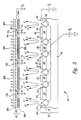
- the preferred display device 50 of Figure 2 is shown in more detail in Figure 3. It includes a baseplate 52 having a plurality of field-induced electron emitters 54 carried by a supporting substrate 56. Each emitter 54 is disposed within a respective aperture in an insulating layer 58 deposited on the surface of the supporting substrate 56. A conductive layer forming an extraction grid 60 is deposited on the insulating layer 58 peripherally about the respective apertures of the emitters 54.
- the preferred display device 50 of Figure 3 also includes a faceplate 62 having a substantially transparent viewing layer 64 positioned in a substantially parallel spaced-apart relationship with the baseplate 52 by spacers (not shown).
- An anode 66 such as an Indium tin oxide layer, having localized portions 66a, 66b, 66c and 66d is deposited on a substantially planar surface of the viewing layer 64 facing the baseplate 52 opposite respective sets of emitters 56a, 56b, 56c and 56d.
- Localized portions of a luminescent layer 68a, 68b, 68c and 68d are each deposited on respective localized portions of the anode 66a, 66b, 66c and 66d.
- the luminescent layer 68a, 68b, 68c, 68d comprises a phosphorescent material which emits light when bombarded by electrons.
- a plurality of focusing electrodes 72a, 72b and 72c comprising conductive strips are deposited on the substantially planar surface of the viewing layer 64 around the periphery of respective localized portions of the anode 66a, 66b, 66c and 66d substantially opposite the respective sets of emitters 54a, 54b, 54c and 54d of the localized portions of the anode 66a, 66b, 66c and 66d.
- a black matrix 70 which can be conductive is deposited on the plurality of focusing electrodes 72a, 72b, and 72c between the localized portions of the anode 66a, 66b, 66c, and 66d.
- an insulating layer 71 encloses each of the focusing electrodes 72a, 72b, and 72c and the black matrix 70.
- a conductive voltage V c such as 40 volts applied to the conductive layer 60 and a source voltage V s such as 0 volts applied to the emitters 54 causes an electron emission to occur from each of the emitters 54 as previously described.
- An anode voltage V a such as 1,000 volts applied to each localized portion of the anode 66a, 66b, 66c and 66d attracts these electron emissions toward the faceplate 62. Some of these electron emissions bombard the localized portions of the luminescent layer 68a, 68b, 68c and 68d and cause these localized portions to emit light and thereby provide a display.
- the display device 50 is shown in Figure 3 having only two emitters 54 associated with each of the localized portions of the luminescent layer 68a, 68b, 68c and 68d for ease of understanding, those with skill in the field of this invention will understand that many more emitters 54 are preferably associated with each of the localized portions of the luminescent layer 68a, 68b, 68c and 68d in order to average out individual differences in the electron emissions from different emitters 54.
- the electron emissions from the emitters 54 attempt to spread out. In the conventional field emission display device this would cause the previously described bleedover.
- a focusing electrode voltage V f such as 500 volts is applied to each of the focusing electrodes 72a, 72b and 72c. Because of the voltage differential between the focusing electrodes 72a, 72b and 72c and the localized portions of the anode 66a, 66b, 66c and 66d, the electron emissions from the emitters 54 are deflected toward their respective localized portion of the anode 66a, 66b, 66c and 66d and are thus prevented from causing bleedover.
- the preferred faceplate 62 of the display device 50 is shown in more detail in Figure 4.
- the localized portions of anode 66a, 66b, 66c and 66d are deposited on the substantially planar surface of the viewing layer 64 and are surrounded by the focusing electrodes 72a, 72b and 72c.
- the black matrix 70 is deposited between the localized portions of the anode 66a, 66b, 66c and 66d.
- three localized portions of the anode can be combined to form one pixel 74 of the color display having a red R, a green G, and a blue B sub-pixel.
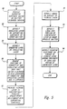
- a method for constructing a display device is shown.
- a supporting substrate having a field-induced electron emitter disposed thereon is provided.
- an insulating layer such as a silicon dioxide dielectric layer, is deposited over the surface of the supporting substrate to cover the emitter.
- a conductive layer is deposited on the insulating layer.
- portions of the conductive and insulating layers are removed so that the emitter is disposed within an aperture in the conductive and insulating layers and is exposed. This is preferably accomplished by etching.
- a substantially transparent viewing layer is provided in a substantially parallel spaced-apart relationship with the supporting substrate and having a surface facing the supporting substrate.
- an anode is deposited on the surface of the viewing layer.
- a localized portion of a luminescent layer is deposited on the anode opposite the emitter.
- a focusing electrode comprising a conductive strip is deposited on the substantially planar surface of the viewing layer around the periphery of the localized portion of the luminescent layer. In this manner a display device may be constructed.
- the present invention thus advantageously provides a field emission display device which successfully prevents bleedover even at high display resolutions by employing an insulated focusing electrode at the anode. It should also be noted that the present invention will correct for the minor misalignments between the emitters and the localized portions of the luminescent layer in a field emission display device which are more likely to occur at higher display resolutions.
Landscapes
- Cathode-Ray Tubes And Fluorescent Screens For Display (AREA)
- Formation Of Various Coating Films On Cathode Ray Tubes And Lamps (AREA)
Claims (17)
- Anzeigenvorrichtung (50), umfassend:dadurch gekennzeichnet, dass die Isolationsschicht die Fokussierelektrode umschließt.eine Basisplatte (52), umfassend:ein Trägersubstrat (56);eine Isolationsschicht (58), die auf der Oberfläche des Trägersubstrats angeordnet ist und in der sich eine Vielzahl von Öffnungen befindet;eine Vielzahl feldinduzierter Elektronenemitter (54), die jeweils vom Trägersubstrat getragen werden und innerhalb einer jeweiligen Öffnung in der Isolationsschicht angeordnet sind; undeine leitende Schicht (60), die auf der Isolationsschicht peripher um die Öffnungen darin herum angeordnet ist, so dass eine Leiterspannung (Vc), die an die leitende Schicht angelegt wird, und eine Quellenspannung (Vs), die an die Emitter angelegt wird, bewirken, dass Elektronenemission von jedem der Emitter auftritt; undeine Frontplatte (62), umfassend:eine im Wesentlichen transparente Sichtschicht (64), die in einer im Wesentlichen parallelen beabstandeten Beziehung zur Basisplatte angeordnet ist und eine im Wesentlichen planare Oberfläche aufweist, die der Basisplatte zugewandt ist;eine Anode (66), die auf der im Wesentlichen planaren Oberfläche der Sichtschicht gegenüber den Emittern angeordnet ist, so dass eine Anodenspannung (Va), die an die Anode angelegt wird, die Elektronenemissionen von den Emittern zur Anode hin lenkt;eine Lumineszenzschicht (68a, 68b, 68c und 68d), die auf der Anode gegenüber den Emittern angeordnet ist, so dass zumindest ein Teil der Elektronenemissionen, die zur Anode hin gelenkt werden, einen lokalen Abschnitt (68a, 68b, 68c, 68d) der Lumineszenzschicht bombardieren und bewirken, dass er Licht aussendet, wodurch eine Anzeige bereitgestellt wird;eine Fokussierelektrode (72a, 72b, 72c), die einen leitenden Streifen umfasst, der auf der im Wesentlichen planaren Oberfläche der Sichtschicht um den Umfang des lokalen Abschnitts der Lumineszenzschicht herum im Wesentlichen gegenüber den Emittern angeordnet ist, so dass eine an die Fokussierelektrode angelegte Fokussierelektrodenspannung (Vf), die geringer ist als die Anodenspannung, die zur Anode hin gelenkten Elektronenemissionen auf den lokalen Abschnitt der Lumineszenzschicht fokussiert; undeine Isolationsschicht (71), die um den Umfang des lokalen Abschnitts der Lumineszenzschicht herum angeordnet ist,
- Anzeigenvorrichtung nach Anspruch 1, worin während der Verwendung die Quellenspannung (Vs), die Anodenspannung (Va), die Fokussierelektrodenspannung (Vf) und die Leiterspannung (Vc) unterschiedlich sind.
- Anzeigenvorrichtung nach Anspruch 1, worin die Lumineszenzschicht (68) eine phosphoreszierende Schicht umfasst.
- Anzeigenvorrichtung nach Anspruch 3, worin die phosphoreszierende Schicht eine Kathodophosphoreszenzschicht umfasst.
- Anzeigenvorrichtung nach Anspruch 1, worin die Lumineszenzschicht (68) eine Vielzahl lokaler Abschnitte (68a-68d) aufweist, die jeweils einem einer Vielzahl von Sätzen der Emitter (54) zugeordnet sind, wobei die Frontplatte weiters eine Vielzahl von Fokussierelektroden (72) umfasst, die jeweils einen leitenden Streifen umfassen, der auf der im Wesentlichen planaren Oberfläche der Sichtschicht um den Umfang eines der Vielzahl lokaler Abschnitte der Lumineszenzschicht herum im Wesentlichen gegenüber den Sätzen der Emitter, die dem lokalen Abschnitt zugeordnet sind, angeordnet ist, so dass eine an die Fokussierelektrode angelegte Fokussierelektrodenspannung, die niedriger ist als die Anodenspannung, die Elektronenemissionen, die zur Anode hin gelenkt sind, von diesen Sätzen der Emitter weg auf den lokalen Abschnitt fokussieren.
- Anzeigenvorrichtung nach Anspruch 5, worin die Anzeigenvorrichtung eine Vielzahl von Pixel aufweist, die jeweils einen der Vielzahl der lokalen Abschnitte (68a-68d) der Lumineszenzschicht umfassen, wobei jedes Pixel dadurch einem der Sätze der Emitter (54) zugeordnet ist, wobei die Basisplatte (52) weiters eine Vielzahl von Emitterleitern umfasst, die jeweils operativ an die Emitter eines der Sätze von Emittern gekoppelt sind, so dass jeder der Sätze von Emittern allein adressierbar ist, indem die Leiterspannung an die leitende Schicht angelegt wird und die Quellenspannung an den Emitterleiter angelegt wird, der operativ an die Emitter des Satzes der Emitter gekoppelt ist.
- Anzeigenvorrichtung nach Anspruch 5, worin die Anzeigenvorrichtung eine Vielzahl von Farbpixel aufweist, die jeweils ein rotes, ein blaues und ein grünes Sub-Pixel umfassen, wobei jedes Sub-Pixel einen der Vielzahl lokaler Abschnitte der Lumineszenzschicht umfasst, wodurch jedes Sub-Pixel einem der Sätze der Emitter zugeordnet ist, wobei die Basisplatte weiters eine Vielzahl von Emitterleitern umfasst, die jeweils operativ an die Emitter eines der Sätze der Emitter gekoppelt sind, so dass jeder Satz der Emitter allein adressierbar ist, indem die Leiterspannung an die leitende Schicht angelegt wird und indem die Quellenspannung an den Emitterleiter angelegt wird, der operativ an die Emitter des Satzes der Emitter gekoppelt ist.
- Anzeigenvorrichtung nach Anspruch 5, worin die Anode (66) eine Vielzahl lokaler Abschnitte (66a - 66d) aufweist, die jeweils allein einem der Vielzahl lokaler Abschnitte (68a - 68d) der Lumineszenzschicht zugeordnet sind.
- Anzeigenvorrichtung nach Anspruch 1, weiters eine schwarze Matrix (70) umfassend, die um den Umfang des lokalen Abschnitts der Lumineszenzschicht herum angeordnet ist.
- Anzeigenvorrichtung nach Anspruch 9, worin die schwarze Matrix elektrisch leitend ist.
- Anzeigenvorrichtung nach Anspruch 9 oder 10, worin die schwarze Matrix auf der Fokussierelektrode (72) angeordnet ist und der Basisplatte (52) zugewandt ist.
- Anzeigenvorrichtung nach einem der Ansprüche 9 bis 11, worin die schwarze Matrix von der Isolationsschicht (71) eingeschlossen ist.
- Elektronisches System (40) zum Bereitstellen einer Anzeige, wobei das elektronische System umfasst:eine Eingabevorrichtung (44);eine Speichervorrichtung (42);einen Prozessor (48), der operativ an die Eingabe- und die Speichervorrichtung gekoppelt ist; sowieeine Anzeigenvorrichtung (50) nach einem der vorangegangenen Ansprüche, wobei die Anzeigenvorrichtung operativ an den Prozessor gekoppelt ist.
- Verfahren zum Konstruieren einer Anzeigenvorrichtung (50), umfassend:das Bereitstellen eines Trägersubstrats (56), auf dem ein feldinduzierter Elektronenemitter (54) angeordnet ist;das Auftragen einer Isolationsschicht (58) auf die Oberfläche des Trägersubstrats, so dass sie den Emitter bedeckt;das Auftragen einer leitenden Schicht (60) auf die Isolationsschicht;das Entfernen von Abschnitten der Leiter- und der Isolationsschicht, so dass der Emitter freiliegt und innerhalb einer Öffnung in der Leiter- und der Isolationsschicht angeordnet ist, wodurch eine Quellenspannung (Vs), die an den Emitter angelegt wird, und eine Leiterspannung (Vc), die an die Leiterschicht angelegt wird, bewirken, dass Elektronenemission aus dem Emitter auftritt;das Bereitstellen einer im Wesentlichen transparenten Sichtschicht (64) in einer im Wesentlichen parallelen beabstandeten Beziehung zum Trägersubstrat, wobei sie eine dem Trägersubstrat zugewandte Oberfläche aufweist;das Bereitstellen einer Anode (66) auf der Oberfläche der Sichtschicht, die dem Emitter gegenüberliegt, so dass eine Anodenspannung (Va), die an die Anode angelegt wird, die Elektronenemission aus dem Emitter zur Anode hin lenkt;das Bereitstellen einer Lumineszenzschicht (68) mit einem lokalen Abschnitt (68a-68d), der auf der Anode gegenüber dem Emitter angeordnet ist, so dass die Elektronenemission, die zur Anode hin gelenkt wird, den lokalen Abschnitt bombardieren kann und bewirken kann, dass er Licht aussendet, wodurch eine Anzeige bereitgestellt wird;das Anordnen einer Fokussierelektrode (72), die einen leitenden Streifen, auf der im Wesentlichen planaren Oberfläche der Sichtschicht um den Umfang des lokalen Abschnitts der Lumineszenzschicht herum im Wesentlichen gegenüber dem Emitter umasst, so dass eine an die Fokussierelektrode angelegte Fokussierelektrodenspannung (Vf), die geringer als die Anodenspannung ist, die zur Anode hin gelenkte Elektronenemission zum lokalen Abschnitt der Lumineszenzschicht fokussiert;und das Einschließen der Fokussierelektrode in einer Isolationsschicht (71).
- Verfahren nach Anspruch 14, weiters umfassend den Schritt des Bereitstellens einer schwarzen Matrix (70) um den Umfang des lokalen Abschnitts der Lumineszenzschicht herum.
- Verfahren nach Anspruch 15, worin die schwarze Matrix so auf der Fokussierelektrode (72) angeordnet wird, dass sie der Basisplatte (52) zugewandt ist.
- Verfahren nach Anspruch 15 oder 16, worin beim Schritt des Einschließens der Fokussierelektrode (72) in der Isolationsschicht (71) auch die schwarze Matrix eingeschlossen wird.
Applications Claiming Priority (3)
| Application Number | Priority Date | Filing Date | Title |
|---|---|---|---|
| US520886 | 1995-08-30 | ||
| US08/520,886 US5773927A (en) | 1995-08-30 | 1995-08-30 | Field emission display device with focusing electrodes at the anode and method for constructing same |
| PCT/US1996/012793 WO1997008731A1 (en) | 1995-08-30 | 1996-08-07 | Field emission display device with focusing electrodes at the anode and method for constructing same |
Publications (2)
| Publication Number | Publication Date |
|---|---|
| EP0847589A1 EP0847589A1 (de) | 1998-06-17 |
| EP0847589B1 true EP0847589B1 (de) | 2001-12-05 |
Family
ID=24074453
Family Applications (1)
| Application Number | Title | Priority Date | Filing Date |
|---|---|---|---|
| EP96927327A Expired - Lifetime EP0847589B1 (de) | 1995-08-30 | 1996-08-07 | Feldemissionsanzeigevorrichtung mit fokusierungelektroden beimder anode und verfahren zu deren herstellung |
Country Status (8)
| Country | Link |
|---|---|
| US (2) | US5773927A (de) |
| EP (1) | EP0847589B1 (de) |
| JP (2) | JP3696887B2 (de) |
| KR (1) | KR19990044246A (de) |
| AU (1) | AU6718896A (de) |
| DE (1) | DE69617704T2 (de) |
| TW (1) | TW319884B (de) |
| WO (1) | WO1997008731A1 (de) |
Families Citing this family (31)
| Publication number | Priority date | Publication date | Assignee | Title |
|---|---|---|---|---|
| US5475705A (en) * | 1993-04-29 | 1995-12-12 | Ericsson Ge Mobile Communications Inc. | Demodulator for Manchester-coded FM signals |
| US5773927A (en) * | 1995-08-30 | 1998-06-30 | Micron Display Technology, Inc. | Field emission display device with focusing electrodes at the anode and method for constructing same |
| US6140986A (en) * | 1997-02-13 | 2000-10-31 | Micron Technology, Inc. | Combined monochrome and color display |
| JP3199682B2 (ja) * | 1997-03-21 | 2001-08-20 | キヤノン株式会社 | 電子放出装置及びそれを用いた画像形成装置 |
| FR2762927A1 (fr) * | 1997-04-30 | 1998-11-06 | Pixtech Sa | Anode d'ecran plat de visualisation |
| US6369497B1 (en) * | 1999-03-01 | 2002-04-09 | Micron Technology, Inc. | Method of fabricating row lines of a field emission array and forming pixel openings therethrough by employing two masks |
| US6008063A (en) * | 1999-03-01 | 1999-12-28 | Micron Technology, Inc. | Method of fabricating row lines of a field emission array and forming pixel openings therethrough |
| WO2001011646A2 (en) * | 1999-08-05 | 2001-02-15 | Ipc-Transtech Display Pte Ltd. | Cathodoluminescent flat panel displays with reduced electron scattering and improved luminance uniformity |
| JP2001188507A (ja) * | 1999-12-28 | 2001-07-10 | Futaba Corp | 蛍光発光型表示器及び蛍光発光型表示装置 |
| KR100499120B1 (ko) * | 2000-02-25 | 2005-07-04 | 삼성에스디아이 주식회사 | 카본 나노튜브를 이용한 3전극 전계 방출 표시소자 |
| US6448717B1 (en) | 2000-07-17 | 2002-09-10 | Micron Technology, Inc. | Method and apparatuses for providing uniform electron beams from field emission displays |
| US6894665B1 (en) | 2000-07-20 | 2005-05-17 | Micron Technology, Inc. | Driver circuit and matrix type display device using driver circuit |
| AU2001280892A1 (en) * | 2000-07-28 | 2002-02-13 | Clairvoyante Laboratories, Inc. | Arrangement of color pixels for full color imaging devices with simplified addressing |
| US7274383B1 (en) * | 2000-07-28 | 2007-09-25 | Clairvoyante, Inc | Arrangement of color pixels for full color imaging devices with simplified addressing |
| US7283142B2 (en) * | 2000-07-28 | 2007-10-16 | Clairvoyante, Inc. | Color display having horizontal sub-pixel arrangements and layouts |
| US7005787B2 (en) * | 2001-01-24 | 2006-02-28 | Industrial Technology Research Institute | Anodic bonding of spacer for field emission display |
| US7123277B2 (en) * | 2001-05-09 | 2006-10-17 | Clairvoyante, Inc. | Conversion of a sub-pixel format data to another sub-pixel data format |
| US7070472B2 (en) * | 2001-08-29 | 2006-07-04 | Motorola, Inc. | Field emission display and methods of forming a field emission display |
| US6891319B2 (en) | 2001-08-29 | 2005-05-10 | Motorola, Inc. | Field emission display and methods of forming a field emission display |
| US6879097B2 (en) * | 2001-09-28 | 2005-04-12 | Candescent Technologies Corporation | Flat-panel display containing electron-emissive regions of non-uniform spacing or/and multi-part lateral configuration |
| AU2002353139A1 (en) * | 2001-12-14 | 2003-06-30 | Clairvoyante Laboratories, Inc. | Improvements to color flat panel display sub-pixel arrangements and layouts with reduced visibility of a blue luminance well |
| US20030117423A1 (en) * | 2001-12-14 | 2003-06-26 | Brown Elliott Candice Hellen | Color flat panel display sub-pixel arrangements and layouts with reduced blue luminance well visibility |
| US7492379B2 (en) | 2002-01-07 | 2009-02-17 | Samsung Electronics Co., Ltd. | Color flat panel display sub-pixel arrangements and layouts for sub-pixel rendering with increased modulation transfer function response |
| US7417648B2 (en) | 2002-01-07 | 2008-08-26 | Samsung Electronics Co. Ltd., | Color flat panel display sub-pixel arrangements and layouts for sub-pixel rendering with split blue sub-pixels |
| US7755652B2 (en) | 2002-01-07 | 2010-07-13 | Samsung Electronics Co., Ltd. | Color flat panel display sub-pixel rendering and driver configuration for sub-pixel arrangements with split sub-pixels |
| US7720541B2 (en) * | 2003-08-18 | 2010-05-18 | Cardiac Pacemakers, Inc. | Adaptive therapy for disordered breathing |
| KR20060037878A (ko) * | 2004-10-29 | 2006-05-03 | 삼성에스디아이 주식회사 | 전자방출 표시장치 |
| KR20060037877A (ko) * | 2004-10-29 | 2006-05-03 | 삼성에스디아이 주식회사 | 전자방출 표시장치 및 이의 제조방법 |
| JP4949083B2 (ja) * | 2007-03-09 | 2012-06-06 | 株式会社ピュアロンジャパン | フィールドエミッションランプ、バックライトユニットおよび表示板 |
| CN102148119B (zh) * | 2010-11-27 | 2012-12-05 | 福州大学 | 发射单元双栅单阴式无介质三极fed装置及其驱动方法 |
| CN102097272B (zh) * | 2011-01-10 | 2012-06-27 | 福州大学 | 阳栅同基板的三极结构场致发射显示器 |
Family Cites Families (16)
| Publication number | Priority date | Publication date | Assignee | Title |
|---|---|---|---|---|
| US3500102A (en) * | 1967-05-15 | 1970-03-10 | Us Army | Thin electron tube with electron emitters at intersections of crossed conductors |
| JPS6188432A (ja) * | 1984-10-08 | 1986-05-06 | Nec Corp | ドツトマトリクス螢光表示管 |
| JPS62290050A (ja) * | 1986-06-07 | 1987-12-16 | Futaba Corp | 蛍光表示管及びその製造方法 |
| FR2623013A1 (fr) * | 1987-11-06 | 1989-05-12 | Commissariat Energie Atomique | Source d'electrons a cathodes emissives a micropointes et dispositif de visualisation par cathodoluminescence excitee par emission de champ,utilisant cette source |
| US5212426A (en) * | 1991-01-24 | 1993-05-18 | Motorola, Inc. | Integrally controlled field emission flat display device |
| WO1992016012A1 (en) * | 1991-03-01 | 1992-09-17 | Seiko Epson Corporation | Light projecting device |
| US5129850A (en) * | 1991-08-20 | 1992-07-14 | Motorola, Inc. | Method of making a molded field emission electron emitter employing a diamond coating |
| US5191217A (en) * | 1991-11-25 | 1993-03-02 | Motorola, Inc. | Method and apparatus for field emission device electrostatic electron beam focussing |
| US5186670A (en) * | 1992-03-02 | 1993-02-16 | Micron Technology, Inc. | Method to form self-aligned gate structures and focus rings |
| US5371431A (en) * | 1992-03-04 | 1994-12-06 | Mcnc | Vertical microelectronic field emission devices including elongate vertical pillars having resistive bottom portions |
| US5359256A (en) * | 1992-07-30 | 1994-10-25 | The United States Of America As Represented By The Secretary Of The Navy | Regulatable field emitter device and method of production thereof |
| JP3252545B2 (ja) * | 1993-07-21 | 2002-02-04 | ソニー株式会社 | 電界放出型カソードを用いたフラットディスプレイ |
| US5541478A (en) * | 1994-03-04 | 1996-07-30 | General Motors Corporation | Active matrix vacuum fluorescent display using pixel isolation |
| US5491376A (en) * | 1994-06-03 | 1996-02-13 | Texas Instruments Incorporated | Flat panel display anode plate having isolation grooves |
| US5508584A (en) * | 1994-12-27 | 1996-04-16 | Industrial Technology Research Institute | Flat panel display with focus mesh |
| US5773927A (en) * | 1995-08-30 | 1998-06-30 | Micron Display Technology, Inc. | Field emission display device with focusing electrodes at the anode and method for constructing same |
-
1995
- 1995-08-30 US US08/520,886 patent/US5773927A/en not_active Expired - Lifetime
-
1996
- 1996-08-07 WO PCT/US1996/012793 patent/WO1997008731A1/en not_active Application Discontinuation
- 1996-08-07 KR KR1019980701482A patent/KR19990044246A/ko active Search and Examination
- 1996-08-07 DE DE69617704T patent/DE69617704T2/de not_active Expired - Lifetime
- 1996-08-07 AU AU67188/96A patent/AU6718896A/en not_active Abandoned
- 1996-08-07 JP JP51028997A patent/JP3696887B2/ja not_active Expired - Fee Related
- 1996-08-07 EP EP96927327A patent/EP0847589B1/de not_active Expired - Lifetime
- 1996-08-28 TW TW085110457A patent/TW319884B/zh not_active IP Right Cessation
-
1998
- 1998-04-06 US US09/055,811 patent/US6242865B1/en not_active Expired - Fee Related
-
2004
- 2004-10-01 JP JP2004290005A patent/JP3813158B2/ja not_active Expired - Fee Related
Also Published As
| Publication number | Publication date |
|---|---|
| US6242865B1 (en) | 2001-06-05 |
| JP2005011823A (ja) | 2005-01-13 |
| US5773927A (en) | 1998-06-30 |
| DE69617704D1 (de) | 2002-01-17 |
| JP3813158B2 (ja) | 2006-08-23 |
| EP0847589A1 (de) | 1998-06-17 |
| TW319884B (de) | 1997-11-11 |
| KR19990044246A (ko) | 1999-06-25 |
| AU6718896A (en) | 1997-03-19 |
| DE69617704T2 (de) | 2002-07-18 |
| WO1997008731A1 (en) | 1997-03-06 |
| JP2002509634A (ja) | 2002-03-26 |
| JP3696887B2 (ja) | 2005-09-21 |
Similar Documents
| Publication | Publication Date | Title |
|---|---|---|
| EP0847589B1 (de) | Feldemissionsanzeigevorrichtung mit fokusierungelektroden beimder anode und verfahren zu deren herstellung | |
| US5015912A (en) | Matrix-addressed flat panel display | |
| US5229691A (en) | Electronic fluorescent display | |
| EP0404022B1 (de) | Flache Bildwiedergabevorrichtung und Verfahren zur Herstellung derselben | |
| US4857799A (en) | Matrix-addressed flat panel display | |
| US5801485A (en) | Display device | |
| US5621284A (en) | Electronic fluorescent display system | |
| US5504387A (en) | Flat display where a first film electrode, a dielectric film, and a second film electrode are successively formed on a base plate and electrons are directly emitted from the first film electrode | |
| US6011567A (en) | Image forming apparatus | |
| JP2001297724A (ja) | 平面ディスプレースクリーン・カソードプレート | |
| US4034255A (en) | Vane structure for a flat image display device | |
| US6843697B2 (en) | Black matrix for flat panel field emission displays | |
| US5565754A (en) | Colour field emission display | |
| US5940163A (en) | Photon coupled color flat panel display and method of manufacture | |
| US6107733A (en) | Anode for a flat display screen | |
| US4099085A (en) | Parallel vane structure for a flat display device | |
| KR100989419B1 (ko) | 더미 전극을 구비한 전계 방출 표시장치 | |
| US20050020176A1 (en) | Field emission device fabrication methods, field emission base plates, and field emission display devices | |
| US20080088220A1 (en) | Electron emission device | |
| KR100378003B1 (ko) | 전계방출소자 | |
| JPH01298628A (ja) | 平板状ディスプレイ装置 | |
| Woodhead | Flat cathode ray tubes | |
| EP1772893A1 (de) | Flachdisplay-einrichtung | |
| JPH11339697A (ja) | 画像表示装置 | |
| JPH0836976A (ja) | 表示装置 |
Legal Events
| Date | Code | Title | Description |
|---|---|---|---|
| PUAI | Public reference made under article 153(3) epc to a published international application that has entered the european phase |
Free format text: ORIGINAL CODE: 0009012 |
|
| 17P | Request for examination filed |
Effective date: 19980319 |
|
| AK | Designated contracting states |
Kind code of ref document: A1 Designated state(s): DE GB IT |
|
| 17Q | First examination report despatched |
Effective date: 19980528 |
|
| GRAG | Despatch of communication of intention to grant |
Free format text: ORIGINAL CODE: EPIDOS AGRA |
|
| GRAG | Despatch of communication of intention to grant |
Free format text: ORIGINAL CODE: EPIDOS AGRA |
|
| GRAG | Despatch of communication of intention to grant |
Free format text: ORIGINAL CODE: EPIDOS AGRA |
|
| GRAH | Despatch of communication of intention to grant a patent |
Free format text: ORIGINAL CODE: EPIDOS IGRA |
|
| GRAH | Despatch of communication of intention to grant a patent |
Free format text: ORIGINAL CODE: EPIDOS IGRA |
|
| RBV | Designated contracting states (corrected) |
Designated state(s): DE GB IT |
|
| GRAA | (expected) grant |
Free format text: ORIGINAL CODE: 0009210 |
|
| AK | Designated contracting states |
Kind code of ref document: B1 Designated state(s): DE GB IT |
|
| REG | Reference to a national code |
Ref country code: GB Ref legal event code: IF02 |
|
| REF | Corresponds to: |
Ref document number: 69617704 Country of ref document: DE Date of ref document: 20020117 |
|
| PLBE | No opposition filed within time limit |
Free format text: ORIGINAL CODE: 0009261 |
|
| STAA | Information on the status of an ep patent application or granted ep patent |
Free format text: STATUS: NO OPPOSITION FILED WITHIN TIME LIMIT |
|
| 26N | No opposition filed | ||
| PGFP | Annual fee paid to national office [announced via postgrant information from national office to epo] |
Ref country code: GB Payment date: 20090805 Year of fee payment: 14 Ref country code: DE Payment date: 20090730 Year of fee payment: 14 |
|
| PGFP | Annual fee paid to national office [announced via postgrant information from national office to epo] |
Ref country code: IT Payment date: 20090814 Year of fee payment: 14 |
|
| GBPC | Gb: european patent ceased through non-payment of renewal fee |
Effective date: 20100807 |
|
| PG25 | Lapsed in a contracting state [announced via postgrant information from national office to epo] |
Ref country code: IT Free format text: LAPSE BECAUSE OF NON-PAYMENT OF DUE FEES Effective date: 20100807 |
|
| REG | Reference to a national code |
Ref country code: DE Ref legal event code: R119 Ref document number: 69617704 Country of ref document: DE Effective date: 20110301 |
|
| PG25 | Lapsed in a contracting state [announced via postgrant information from national office to epo] |
Ref country code: DE Free format text: LAPSE BECAUSE OF NON-PAYMENT OF DUE FEES Effective date: 20110301 |
|
| PG25 | Lapsed in a contracting state [announced via postgrant information from national office to epo] |
Ref country code: GB Free format text: LAPSE BECAUSE OF NON-PAYMENT OF DUE FEES Effective date: 20100807 |