EP0845770A1 - Dispositif d'affichage électroluminescent organique - Google Patents
Dispositif d'affichage électroluminescent organique Download PDFInfo
- Publication number
- EP0845770A1 EP0845770A1 EP97120761A EP97120761A EP0845770A1 EP 0845770 A1 EP0845770 A1 EP 0845770A1 EP 97120761 A EP97120761 A EP 97120761A EP 97120761 A EP97120761 A EP 97120761A EP 0845770 A1 EP0845770 A1 EP 0845770A1
- Authority
- EP
- European Patent Office
- Prior art keywords
- organic
- display apparatus
- type fet
- layer
- filter
- Prior art date
- Legal status (The legal status is an assumption and is not a legal conclusion. Google has not performed a legal analysis and makes no representation as to the accuracy of the status listed.)
- Withdrawn
Links
- 238000005401 electroluminescence Methods 0.000 title claims description 96
- 239000000758 substrate Substances 0.000 claims abstract description 28
- 239000003990 capacitor Substances 0.000 claims abstract description 7
- 239000000203 mixture Substances 0.000 claims abstract description 4
- VYPSYNLAJGMNEJ-UHFFFAOYSA-N silicon dioxide Inorganic materials O=[Si]=O VYPSYNLAJGMNEJ-UHFFFAOYSA-N 0.000 claims description 27
- 229910021420 polycrystalline silicon Inorganic materials 0.000 claims description 12
- 229920005591 polysilicon Polymers 0.000 claims description 12
- XUIMIQQOPSSXEZ-UHFFFAOYSA-N Silicon Chemical compound [Si] XUIMIQQOPSSXEZ-UHFFFAOYSA-N 0.000 claims description 8
- 229910021417 amorphous silicon Inorganic materials 0.000 claims description 8
- 229910052710 silicon Inorganic materials 0.000 claims description 8
- 239000010703 silicon Substances 0.000 claims description 8
- 239000011521 glass Substances 0.000 claims description 7
- 239000010453 quartz Substances 0.000 claims description 5
- PNEYBMLMFCGWSK-UHFFFAOYSA-N aluminium oxide Inorganic materials [O-2].[O-2].[O-2].[Al+3].[Al+3] PNEYBMLMFCGWSK-UHFFFAOYSA-N 0.000 claims description 3
- 239000000919 ceramic Substances 0.000 claims description 3
- 239000013078 crystal Substances 0.000 claims description 3
- 229920001296 polysiloxane Polymers 0.000 claims 1
- 239000010410 layer Substances 0.000 description 63
- 229910052681 coesite Inorganic materials 0.000 description 12
- 229910052906 cristobalite Inorganic materials 0.000 description 12
- 229910052682 stishovite Inorganic materials 0.000 description 12
- 229910052905 tridymite Inorganic materials 0.000 description 12
- 238000010586 diagram Methods 0.000 description 11
- 239000000377 silicon dioxide Substances 0.000 description 10
- 239000000463 material Substances 0.000 description 9
- 238000004519 manufacturing process Methods 0.000 description 8
- 238000002347 injection Methods 0.000 description 7
- 239000007924 injection Substances 0.000 description 7
- 239000010408 film Substances 0.000 description 6
- 239000000126 substance Substances 0.000 description 6
- 230000005525 hole transport Effects 0.000 description 5
- 229910052751 metal Inorganic materials 0.000 description 4
- 239000002184 metal Substances 0.000 description 4
- 239000010409 thin film Substances 0.000 description 4
- 239000007789 gas Substances 0.000 description 3
- 230000010354 integration Effects 0.000 description 3
- 239000011229 interlayer Substances 0.000 description 3
- 239000011159 matrix material Substances 0.000 description 3
- 230000002093 peripheral effect Effects 0.000 description 3
- 229920001721 polyimide Polymers 0.000 description 3
- 239000004642 Polyimide Substances 0.000 description 2
- 230000002411 adverse Effects 0.000 description 2
- 238000005229 chemical vapour deposition Methods 0.000 description 2
- PJXISJQVUVHSOJ-UHFFFAOYSA-N indium(III) oxide Inorganic materials [O-2].[O-2].[O-2].[In+3].[In+3] PJXISJQVUVHSOJ-UHFFFAOYSA-N 0.000 description 2
- 238000000034 method Methods 0.000 description 2
- 229910021421 monocrystalline silicon Inorganic materials 0.000 description 2
- 239000007790 solid phase Substances 0.000 description 2
- XOLBLPGZBRYERU-UHFFFAOYSA-N tin dioxide Chemical compound O=[Sn]=O XOLBLPGZBRYERU-UHFFFAOYSA-N 0.000 description 2
- 239000005725 8-Hydroxyquinoline Substances 0.000 description 1
- UFHFLCQGNIYNRP-UHFFFAOYSA-N Hydrogen Chemical compound [H][H] UFHFLCQGNIYNRP-UHFFFAOYSA-N 0.000 description 1
- OAICVXFJPJFONN-UHFFFAOYSA-N Phosphorus Chemical compound [P] OAICVXFJPJFONN-UHFFFAOYSA-N 0.000 description 1
- 229910007264 Si2H6 Inorganic materials 0.000 description 1
- 229910052581 Si3N4 Inorganic materials 0.000 description 1
- 239000007983 Tris buffer Substances 0.000 description 1
- 239000004411 aluminium Substances 0.000 description 1
- 229910052782 aluminium Inorganic materials 0.000 description 1
- XAGFODPZIPBFFR-UHFFFAOYSA-N aluminium Chemical compound [Al] XAGFODPZIPBFFR-UHFFFAOYSA-N 0.000 description 1
- 239000012298 atmosphere Substances 0.000 description 1
- 230000015572 biosynthetic process Effects 0.000 description 1
- 230000007547 defect Effects 0.000 description 1
- PZPGRFITIJYNEJ-UHFFFAOYSA-N disilane Chemical compound [SiH3][SiH3] PZPGRFITIJYNEJ-UHFFFAOYSA-N 0.000 description 1
- 239000002019 doping agent Substances 0.000 description 1
- 238000001312 dry etching Methods 0.000 description 1
- 238000005538 encapsulation Methods 0.000 description 1
- 230000002708 enhancing effect Effects 0.000 description 1
- 238000005530 etching Methods 0.000 description 1
- 125000001495 ethyl group Chemical group [H]C([H])([H])C([H])([H])* 0.000 description 1
- 230000001747 exhibiting effect Effects 0.000 description 1
- 230000002349 favourable effect Effects 0.000 description 1
- -1 for example Substances 0.000 description 1
- 239000001257 hydrogen Substances 0.000 description 1
- 229910052739 hydrogen Inorganic materials 0.000 description 1
- 238000005984 hydrogenation reaction Methods 0.000 description 1
- 239000012535 impurity Substances 0.000 description 1
- AMGQUBHHOARCQH-UHFFFAOYSA-N indium;oxotin Chemical compound [In].[Sn]=O AMGQUBHHOARCQH-UHFFFAOYSA-N 0.000 description 1
- 150000002500 ions Chemical class 0.000 description 1
- WABPQHHGFIMREM-UHFFFAOYSA-N lead(0) Chemical compound [Pb] WABPQHHGFIMREM-UHFFFAOYSA-N 0.000 description 1
- 238000003754 machining Methods 0.000 description 1
- 125000002496 methyl group Chemical group [H]C([H])([H])* 0.000 description 1
- 239000012299 nitrogen atmosphere Substances 0.000 description 1
- 229960003540 oxyquinoline Drugs 0.000 description 1
- 229910052698 phosphorus Inorganic materials 0.000 description 1
- 239000011574 phosphorus Substances 0.000 description 1
- 238000005268 plasma chemical vapour deposition Methods 0.000 description 1
- 239000009719 polyimide resin Substances 0.000 description 1
- MCJGNVYPOGVAJF-UHFFFAOYSA-N quinolin-8-ol Chemical compound C1=CN=C2C(O)=CC=CC2=C1 MCJGNVYPOGVAJF-UHFFFAOYSA-N 0.000 description 1
- 239000004065 semiconductor Substances 0.000 description 1
- 238000000926 separation method Methods 0.000 description 1
- HQVNEWCFYHHQES-UHFFFAOYSA-N silicon nitride Chemical compound N12[Si]34N5[Si]62N3[Si]51N64 HQVNEWCFYHHQES-UHFFFAOYSA-N 0.000 description 1
- 238000004544 sputter deposition Methods 0.000 description 1
- 239000007858 starting material Substances 0.000 description 1
- 238000007740 vapor deposition Methods 0.000 description 1
- YVTHLONGBIQYBO-UHFFFAOYSA-N zinc indium(3+) oxygen(2-) Chemical compound [O--].[Zn++].[In+3] YVTHLONGBIQYBO-UHFFFAOYSA-N 0.000 description 1
- XLOMVQKBTHCTTD-UHFFFAOYSA-N zinc oxide Inorganic materials [Zn]=O XLOMVQKBTHCTTD-UHFFFAOYSA-N 0.000 description 1
- 239000011787 zinc oxide Substances 0.000 description 1
Images


Classifications
-
- G—PHYSICS
- G09—EDUCATION; CRYPTOGRAPHY; DISPLAY; ADVERTISING; SEALS
- G09G—ARRANGEMENTS OR CIRCUITS FOR CONTROL OF INDICATING DEVICES USING STATIC MEANS TO PRESENT VARIABLE INFORMATION
- G09G3/00—Control arrangements or circuits, of interest only in connection with visual indicators other than cathode-ray tubes
- G09G3/20—Control arrangements or circuits, of interest only in connection with visual indicators other than cathode-ray tubes for presentation of an assembly of a number of characters, e.g. a page, by composing the assembly by combination of individual elements arranged in a matrix no fixed position being assigned to or needed to be assigned to the individual characters or partial characters
- G09G3/22—Control arrangements or circuits, of interest only in connection with visual indicators other than cathode-ray tubes for presentation of an assembly of a number of characters, e.g. a page, by composing the assembly by combination of individual elements arranged in a matrix no fixed position being assigned to or needed to be assigned to the individual characters or partial characters using controlled light sources
- G09G3/30—Control arrangements or circuits, of interest only in connection with visual indicators other than cathode-ray tubes for presentation of an assembly of a number of characters, e.g. a page, by composing the assembly by combination of individual elements arranged in a matrix no fixed position being assigned to or needed to be assigned to the individual characters or partial characters using controlled light sources using electroluminescent panels
- G09G3/32—Control arrangements or circuits, of interest only in connection with visual indicators other than cathode-ray tubes for presentation of an assembly of a number of characters, e.g. a page, by composing the assembly by combination of individual elements arranged in a matrix no fixed position being assigned to or needed to be assigned to the individual characters or partial characters using controlled light sources using electroluminescent panels semiconductive, e.g. using light-emitting diodes [LED]
- G09G3/3208—Control arrangements or circuits, of interest only in connection with visual indicators other than cathode-ray tubes for presentation of an assembly of a number of characters, e.g. a page, by composing the assembly by combination of individual elements arranged in a matrix no fixed position being assigned to or needed to be assigned to the individual characters or partial characters using controlled light sources using electroluminescent panels semiconductive, e.g. using light-emitting diodes [LED] organic, e.g. using organic light-emitting diodes [OLED]
- G09G3/3225—Control arrangements or circuits, of interest only in connection with visual indicators other than cathode-ray tubes for presentation of an assembly of a number of characters, e.g. a page, by composing the assembly by combination of individual elements arranged in a matrix no fixed position being assigned to or needed to be assigned to the individual characters or partial characters using controlled light sources using electroluminescent panels semiconductive, e.g. using light-emitting diodes [LED] organic, e.g. using organic light-emitting diodes [OLED] using an active matrix
- G09G3/3233—Control arrangements or circuits, of interest only in connection with visual indicators other than cathode-ray tubes for presentation of an assembly of a number of characters, e.g. a page, by composing the assembly by combination of individual elements arranged in a matrix no fixed position being assigned to or needed to be assigned to the individual characters or partial characters using controlled light sources using electroluminescent panels semiconductive, e.g. using light-emitting diodes [LED] organic, e.g. using organic light-emitting diodes [OLED] using an active matrix with pixel circuitry controlling the current through the light-emitting element
-
- G—PHYSICS
- G09—EDUCATION; CRYPTOGRAPHY; DISPLAY; ADVERTISING; SEALS
- G09G—ARRANGEMENTS OR CIRCUITS FOR CONTROL OF INDICATING DEVICES USING STATIC MEANS TO PRESENT VARIABLE INFORMATION
- G09G2300/00—Aspects of the constitution of display devices
- G09G2300/08—Active matrix structure, i.e. with use of active elements, inclusive of non-linear two terminal elements, in the pixels together with light emitting or modulating elements
- G09G2300/0809—Several active elements per pixel in active matrix panels
- G09G2300/0842—Several active elements per pixel in active matrix panels forming a memory circuit, e.g. a dynamic memory with one capacitor
-
- G—PHYSICS
- G09—EDUCATION; CRYPTOGRAPHY; DISPLAY; ADVERTISING; SEALS
- G09G—ARRANGEMENTS OR CIRCUITS FOR CONTROL OF INDICATING DEVICES USING STATIC MEANS TO PRESENT VARIABLE INFORMATION
- G09G2320/00—Control of display operating conditions
- G09G2320/02—Improving the quality of display appearance
- G09G2320/0271—Adjustment of the gradation levels within the range of the gradation scale, e.g. by redistribution or clipping
- G09G2320/0276—Adjustment of the gradation levels within the range of the gradation scale, e.g. by redistribution or clipping for the purpose of adaptation to the characteristics of a display device, i.e. gamma correction
-
- H—ELECTRICITY
- H10—SEMICONDUCTOR DEVICES; ELECTRIC SOLID-STATE DEVICES NOT OTHERWISE PROVIDED FOR
- H10K—ORGANIC ELECTRIC SOLID-STATE DEVICES
- H10K59/00—Integrated devices, or assemblies of multiple devices, comprising at least one organic light-emitting element covered by group H10K50/00
- H10K59/10—OLED displays
- H10K59/12—Active-matrix OLED [AMOLED] displays
- H10K59/123—Connection of the pixel electrodes to the thin film transistors [TFT]
-
- H—ELECTRICITY
- H10—SEMICONDUCTOR DEVICES; ELECTRIC SOLID-STATE DEVICES NOT OTHERWISE PROVIDED FOR
- H10K—ORGANIC ELECTRIC SOLID-STATE DEVICES
- H10K59/00—Integrated devices, or assemblies of multiple devices, comprising at least one organic light-emitting element covered by group H10K50/00
- H10K59/30—Devices specially adapted for multicolour light emission
- H10K59/38—Devices specially adapted for multicolour light emission comprising colour filters or colour changing media [CCM]
Definitions
- the present invention relates to an active matrix organic EL (Electro Luminescence) display apparatus, and more particularly to an organic EL display apparatus which is small in size and highly integrated.
- active matrix organic EL Electro Luminescence
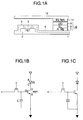
- a color organic EL display apparatus as illustrated in Fig. 7A, has a thin film transistor (hereinafter referred to as "TFT") 41 formed on a quartz or glass substrate 40 as well as a filter 45, a transparent electrode 42 made of a material such as ITO (Indium Tin Oxide), an organic EL layer 43 composed of a hole transport layer, a light emitting layer, an electron transport layer and so on, and a cathode 44 made of a material such as Ag-Mg formed on the same substrate 40.
- TFT thin film transistor
- Fig. 7A is a schematic diagram illustrating one unit of R, G, B pixels constituting one pixel of a color organic EL display apparatus.
- a large step-like difference is formed in a wire 46 which connects the TFT 41 to the transparent electrode 42 of the organic EL element.
- the filter 45 is positioned on the rear surface of the substrate 40 opposite to the surface on which the organic EL element is formed, as illustrated in Fig. 7B, for purposes of eliminating the drawback mentioned above, the thickness of the substrate 40 causes emitted light to spread, so that the size of one pixel is larger and the resolution is degraded.
- the TFT 41 is connected to the transparent electrode 42, which serves as an anode of the organic EL element, and the TFT 41 is formed of a P-type FET since the transparent electrode 42 performing a hole injecting function through the boundary with the organic EL layer.
- an active matrix EL image display apparatus comprising pixels each of which is formed of a thin film EL element, a non-linear element such as the above-mentioned TFT for controlling light emission for an EL element, a capacitor connected to a gate electrode of the non-linear element for holding a signal, and a non-linear element for writing data into the capacitor
- the intensity of light emitted from the organic EL is determined by a current, which flows into the non-linear element for controlling the light emission, where the current is controlled by a voltage accumulated in the capacitor for holding a signal
- An organic EL element has a structure, for example, composed of a substrate, an anode / a hole injection layer / a light emitting layer / an electron transport layer / a cathode, wherein an organic composition is used at least in the light emitting layer. While the hole injection layer and the electron transport layer are not necessarily provided, they are desirable for improving the light emitting performance.
- the element is separated by performing fine machining on the anode, while one terminal of the non-linear element for controlling the light emission such as TFT is connected to the anode by performing element separation (see USP No. 5,550,066).
- a source electrode of the FET is connected to the anode of the organic EL element due to the nature of the N-type FET. As illustrated in Fig. 7C, this connection forms a source follower circuit of the N-type FET including the organic EL element as a load.
- an image display apparatus employing this circuit requires a correcting means in a peripheral circuit for inputting a non-linearly corrected image signal, or the like in order to realize a good gradation representation.
- the addition of such a correcting means results in an increase in cost of the entire image display apparatus.
- the anode of the organic EL element is connected to a drain electrode of the FET due to the nature of the P-type FET.
- These elements form a source-grounded circuit of the P-type FET including the organic EL element as a load.
- an image signal may only be linearly amplified to a value appropriate to the circuit and then inputted thereto. It should be noted however that since the P-type FET is inferior in mobility to the N-type FET, the size of the P-type FET must be larger for providing good characteristics. In addition, the P-type FET is not appropriate to a high resolution image display apparatus.
- the high-temperature resistance of the organic EL material is approximately 100°C.
- color resists when applied on a substrate for forming color filters, they must be baked at temperatures ranging from 120 to 150°C. Thus, a problem arises in that the baking adversely affects the organic EL element.
- an N-type FET 2 is formed on a substrate 1 made of quartz, glass, ceramic, alumina, or the like, as illustrated in Fig. 1A.
- the N-type FET 2 is provided with a gate electrode 3 and wires 4, 5.
- An organic EL element 10 comprising a cathode 7, an organic EL layer 8, and a transparent electrode 9 is arranged on the wire 4 on the drain side.
- a transparent plate 12 such as a glass plate, on which a color filter 11 is formed opposite to the transparent electrode 9 which functions as an anode of the organic EL element.
- the cathode 7 is formed, for example, of an AgMg electrode, the organic EL layer is composed of an electron transport layer, a light emitting layer, a hole injection layer and so on, and the transparent electrode 9, i.e., the anode, is made, for example, of IZO (indium zinc oxide).
- the organic El element is separated by the cathode 7.
- the N-type FET has its drain electrode connected to the cathode 7 of the organic EL element 10 due to the nature of the N-type FET.
- a source grounded circuit of the N-type FET is configured with the organic EL element 10 included as a load element, as illustrated in Fig. 1B.
- an image signal may be linearly amplified to a value appropriate to the circuit and then inputted thereto.
- an image signal For displaying a signal in accordance with the NTSC standard, an image signal has been applied with ⁇ correction with a supposed ⁇ value being 2.2 or less when it is outputted from an image device.
- the ⁇ characteristic of the luminance for an input signal voltage of an image display apparatus using a source grounded circuit of an N-type FET, including the organic EL element as a load is approximately two which is close to the supposed ⁇ value, so that favorable gradation can be provided only by linearly amplifying the image signal to a value appropriate to this circuit.
- a drain electrode of an N-type FET is connected to a cathode of an organic EL element, and a load having a good linear load characteristic is arranged at a source electrode of the N-type FET.
- a source grounded circuit of the N-type FET including a load element having good linearity is configured as illustrated in Fig. 1C.
- polysilicon or a source resistor of the FET may be utilized.
- the ⁇ characteristic of the luminance to an input signal voltage to an image display apparatus using this circuit is one and coincident with the ⁇ value of an image system, so that good gradation can be realized only by linearly amplifying an image signal to a value appropriate to the circuit.
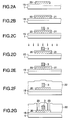
- Figs. 2A - 2G are explanatory diagrams for illustrating various steps of manufacturing an N-type FET used in the present invention
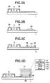
- Figs. 3A - 3D are explanatory diagrams for showing how an organic EL element is formed for the FET
- Fig. 4 is a graph for explaining the light emitting characteristics of the organic EL element used in the present invention
- Fig. 5 is a cross-sectional view illustrating color filters used in the present invention
- Fig. 6 is a perspective view showing how the organic EL element and the color filters are combined in the present invention.
- a SiO 2 layer 15 is formed on a quartz or glass substrate 1, for example, by a sputtering method in a thickness of approximately 1000 ⁇ . Then, an amorphous silicon layer is formed on the SiO 2 layer, for example, by a CVD method in a thickness of approximately 1000 ⁇ .
- These layers are formed under conditions, for example, as follows:
- the amorphous silicon layer is grown in a solid phase to be transformed into a polysilicon layer.
- the solid phase growth is performed under conditions, for example, as follows:
- the polysilicon layer is patterned to form an active silicon layer 20 (Fig. 2A).
- a Si0 2 layer eventually serving as a gate oxide film 21, is formed on the active silicon layer 20, for example, by a plasma CVD method in a thickness of approximately 1000 ⁇ .
- the Si0 2 layer is formed under conditions, for example, as follows:
- an amorphous silicon layer is formed on the SiO 2 layer 21 by a CVD method in a thickness of approximately 4000 ⁇ , for example, under the same conditions as the aforementioned step of Fig. 2A.
- the amorphous silicon layer is annealed, for example, under the same conditions as the aforementioned step of Fig. 2A to form a polysilicon layer which eventually serves as the gate electrode 3.
- the polysilicon layer and the SiO 2 layer formed in the above step of Fig. 2B are patterned together, for example, by dry etching to form the gate electrode 3 and the gate oxide film 21.
- the gate electrode 3 is used as a mask to dope an N-type impurity, for example, phosphorus (P) into regions within the silicon active layer 20, which are to function as a source region and a drain region, by an ion doping method.
- an N-type impurity for example, phosphorus (P)
- the structure is annealed in a nitrogen atmosphere at approximately 550°C for five hours to activate the dopants.
- the structure is further annealed in a hydrogen atmosphere at approximately 400°C for 30 minutes for hydrogenation to reduce a defect level density of the semiconductor.
- a SiO 2 layer eventually serving as an inter-layer insulating layer 22, is formed over the entire substrate in a thickness of approximately 4000 ⁇ , with TEOS used as a starting material.
- the SiO 2 layer serving as the inter-layer insulating layer 22 is formed under conditions, for example, as follows:
- the SiO 2 layer eventually serving as the inter-layer insulating layer 22 is formed with a hole 23 for etching contact.
- Al ⁇ Mg metal (Mg: 90 mole percent) 25, eventually serving as a cathode, is vapor deposited in a region in which the organic EL element is positioned.
- Al ⁇ Mg metal Mg: 90 mole percent
- any material having a work function equal to or lower than approximately 4 eV may be used instead of the Al ⁇ Mg metal.
- wire portions are patterned.
- Polyimide 26 is covered over the region in which the organic EL element is positioned, while the Al ⁇ Mg metal is exposed only for a light emitting portion (see Fig. 3C).
- the Al ⁇ Mg metal 25 in the light emitting portion is sputter etched in a multi-chamber to etch an oxide film on the surface thereof.
- DQX as represented by Chemical Formula 1 for constituting an electron transport layer 8-1 DPA as represented by Chemical Formula 2 for constituting a light emitting layer 8-2
- TPD as represented by Chemical Formula 3 for constituting a hole transport layer 8-3
- MTDATA as represented by Chemical Formula 4 for constituting a hole injection layer 8-4 are formed in this order, for example, by vapor deposition to form the organic EL layers.
- Rn represents a methyl group or an ethyl group.
- a transparent conductive film, IZO 9 (In 2 O 3 ⁇ ZnO (5 mol%) is formed as an anode on the organic EL layers, and a SiO 2 film 10 is formed on the IZO 9 for SiO 2 encapsulation to connect the organic EL element to a drain side of the N-type FET, as illustrated in Fig. 3D.
- a load resistor exhibiting a linear characteristic is implemented by using the gate polysilicon or the active silicon of the N-type FET.
- ITO In 2 O 3 , SnO 2 (10 mol%)
- the like may be employed as the transparent conductive film instead of IZO.
- the organic EL element exhibits waveform versus output intensity characteristics (relative value) as illustrated in Fig. 4 and emits blue green light.
- a color filter for use in this organic EL element is such one as illustrated in Fig. 5 which has a read filter 31, a green filter 32, and a blue filter 33 arranged on a glass plate 30.
- a fluorescent filter 34 is stacked only on the red filter 31.
- the color filter as illustrated in Fig. 5 is aligned to the substrate 1 on which the N-type FET and the organic EL element have been formed as illustrated in Fig. 3H, and both are bonded.
- the substrate 1, FET, fluorescent filter 34, and so on are omitted from Fig. 6.
- the AlMg cathode is separated into regions 7-1, 7-2, 7-3 corresponding to N-type FETs for controlling R, G, B. Therefore, this organic EL element has a separate cathode configuration.
- the present invention is not limited to this particular material.
- the TFT may be formed of crystal silicon or amorphous silicon.
- crystal silicon When crystal silicon is used, a high mobility N-type FET can be provided, so that the size of the N-type FET can be reduced.
- amorphous silicon When using amorphous silicon, the N-type FET can be formed at a lower cost.
- the present invention is not limited to this particular substrate.
- the conventional organic EL display apparatus light is emitted through a transparent substrate, whereas in the structure of the present invention, the light emitting surface is positioned on the opposite surface, so that the substrate need not be transparent. It is therefore possible to use a ceramic substrate, an alumina substrate, or the like as long as it has required mechanical strength, flatness, and high-temperature resistance.
- a source resistor is used as a linear load connected to a source electrode
- the present invention is not limited to this load.
- a load having linear characteristics may be connected to the source electrode using an N-type polysilicon for the lead wire.
- a load resistor may be formed of gate polysilicon.
- the aforementioned polyimide resin (polyimide 26 shown in Fig. 3C) is provided for separating a light emitting element, and may be formed using SiO 2 , silicon nitride, or the like.
- the organic EL element has been described as having an anode - a hole injection layer - a hole transport layer - a light emitting layer - an electron transport layer - a cathode, the present invention is not of course limited to this particular structure of organic EL element.
- the organic EL element may be formed of an anode - a hole transport layer - a light emitting layer - an electron transport layer - a cathode, an anode - a light emitting layer - an electron injection layer - a cathode, or any other appropriate structure.
- a portion for controlling the organic EL element can be entirely formed of high mobility N-type FETs, it is possible to provide a reduced size, a higher integration degree, and an improved resolution at a lower manufacturing cost.
- an organic EL element for emitting blue green light that exhibits the characteristics as illustrated in Fig. 4
- the present invention is not of course limited to this particular type of organic EL element.
- a variety of other organic EL elements may be used, for example, an organic EL element for emitting white light which is provided with a RGB color filter, an organic EL element for emitting blue light which is provided with G, R fluorescent filters and a RGB color filter overlying the fluorescent filters, and an organic EL element for emitting blue light and red light which is provided with a G fluorescent filter and a RGB color filter overlying the fluorescent filter.
- n-type amorphous SiC When n-type amorphous SiC is used as an electron injection layer, p-type amorphous SiC is used as a hole transport layer, and tris(8-hydroxyquinoline) aluminium represented by the following Chemical Formula 5 is used as a light emitting layer, a mixture of n-type amorphous SiC and p-type amorphous SiC may be used as a light emitting layer.
- a cathode of a non-linear element for controlling light emission of an organic EL element is connected to the drain side of an N-type FET, a light emission control circuit for the organic EL element can be formed of a high mobility N-type FET, thereby making it possible to provide an organic EL display apparatus having a higher integration degree, a smaller size, and an improved resolution.
- the N-type FET is formed of single crystal silicon, the resulting light emission control circuit exhibits a particularly high mobility, thereby making it possible to provide a small and high resolution organic EL display apparatus with a much higher integration degree.
- the N-type FET is formed of polysilicon, a high mobility light emission control circuit can be reduced in size.
- an arbitrary substrate may be used unlike the case where single crystal silicon is used, so that selection freedom can be increased for the substrate.
- the N-type FET is formed of amorphous silicon, a high mobility light emission control circuit can be configured using an inexpensive substrate.
- the organic EL element and the color filter can be formed on separate substrates. For this reason, the yield can be improved as compared with the formation of those components on the same substrate wherein an overall yield is calculated by accumulating yields at respective manufacturing processes.
- the high-temperature resistance of the current organic EL material is approximately 100°C.
- color resists When color resists are applied for forming a color filter on the organic EL material, they must be baked at 120°C - 150°C. Thus, it has been quite difficult for the prior art to form the color filter without adversely affecting the organic EL material.
- the present invention can manufacture these components separately, it is possible to provide a good organic EL display apparatus at a high yield because the organic EL element is not deteriorated by the baking of color resists.
- the load can be formed by ordinary silicon TFT manufacturing techniques without using special materials or manufacturing steps.
- the circuit can be operated without additionally providing a special load in the circuit.
Landscapes
- Engineering & Computer Science (AREA)
- Physics & Mathematics (AREA)
- Computer Hardware Design (AREA)
- General Physics & Mathematics (AREA)
- Theoretical Computer Science (AREA)
- Electroluminescent Light Sources (AREA)
- Devices For Indicating Variable Information By Combining Individual Elements (AREA)
Applications Claiming Priority (2)
| Application Number | Priority Date | Filing Date | Title |
|---|---|---|---|
| JP8319307A JPH10161563A (ja) | 1996-11-29 | 1996-11-29 | 有機el表示装置 |
| JP319307/96 | 1996-11-29 |
Publications (1)
| Publication Number | Publication Date |
|---|---|
| EP0845770A1 true EP0845770A1 (fr) | 1998-06-03 |
Family
ID=18108742
Family Applications (1)
| Application Number | Title | Priority Date | Filing Date |
|---|---|---|---|
| EP97120761A Withdrawn EP0845770A1 (fr) | 1996-11-29 | 1997-11-26 | Dispositif d'affichage électroluminescent organique |
Country Status (2)
| Country | Link |
|---|---|
| EP (1) | EP0845770A1 (fr) |
| JP (1) | JPH10161563A (fr) |
Cited By (14)
| Publication number | Priority date | Publication date | Assignee | Title |
|---|---|---|---|---|
| DE19950839A1 (de) * | 1999-10-21 | 2001-05-23 | Fraunhofer Ges Forschung | Vorrichtung zur Ansteuerung der Anzeigeelemente eines Anzeigeelementenarrays und Verfahren zur Herstellung derselben |
| US6350996B1 (en) * | 1998-04-24 | 2002-02-26 | Canon Kabushiki Kaisha | Light emitting diode device |
| WO2003056539A1 (fr) * | 2001-12-28 | 2003-07-10 | Osram Opto Semiconductors Gmbh | Circuit d'attaque a transistors a couches minces et a source de tension pour afficheurs electroluminescents a matrice active |
| US6949879B1 (en) | 1999-04-07 | 2005-09-27 | Microemissive Displays Limited | Optoelectronic display |
| CN100358172C (zh) * | 2004-04-14 | 2007-12-26 | 友达光电股份有限公司 | 有源式有机电致发光元件及其制造方法 |
| US7518146B2 (en) | 1999-09-17 | 2009-04-14 | Semiconductor Energy Laboratory Co., Ltd. | EL display device including color filter and light shielding film |
| EP2073190A1 (fr) * | 2007-12-21 | 2009-06-24 | Commissariat à l'Energie Atomique | Dispositif d'affichage comportant des filtres colorés et des éléments photoémissifs alignés électroniquement |
| EP1732058A3 (fr) * | 2001-01-04 | 2010-02-17 | TPO Displays Corp. | Circuit de pixels a diode electroluminescente organique a faible consomation d'energie |
| US7989812B2 (en) | 1999-10-12 | 2011-08-02 | Semiconductor Energy Laboratory Co., Ltd. | EL display device and a method of manufacturing the same |
| US7995010B2 (en) | 2000-02-29 | 2011-08-09 | Semiconductor Energy Laboratory Co., Ltd. | Light-emitting device |
| US8436790B2 (en) | 1999-09-24 | 2013-05-07 | Semiconductor Energy Laboratory Co., Ltd. | EL display device and electronic device |
| US8466482B2 (en) | 2000-02-01 | 2013-06-18 | Semiconductor Energy Laboratory Co., Ltd. | Semiconductor device and manufacturing method thereof |
| US8956895B2 (en) | 2000-04-25 | 2015-02-17 | Semiconductor Energy Laboratory Co., Ltd. | Light emitting device |
| US20230049123A1 (en) * | 2021-08-10 | 2023-02-16 | Innolux Corporation | Electronic device and manufacturing method and inspection method thereof |
Families Citing this family (10)
| Publication number | Priority date | Publication date | Assignee | Title |
|---|---|---|---|---|
| JP3203227B2 (ja) * | 1998-02-27 | 2001-08-27 | 三洋電機株式会社 | 表示装置の製造方法 |
| JPH11251059A (ja) * | 1998-02-27 | 1999-09-17 | Sanyo Electric Co Ltd | カラー表示装置 |
| JP2000077191A (ja) * | 1998-08-31 | 2000-03-14 | Sanyo Electric Co Ltd | 表示装置 |
| JP2001035663A (ja) * | 1999-07-27 | 2001-02-09 | Pioneer Electronic Corp | 有機エレクトロルミネッセンス素子表示装置及びその製造方法 |
| JP2001035662A (ja) * | 1999-07-27 | 2001-02-09 | Pioneer Electronic Corp | 有機エレクトロルミネッセンス素子表示装置及びその製造方法 |
| TW465122B (en) * | 1999-12-15 | 2001-11-21 | Semiconductor Energy Lab | Light-emitting device |
| US6995736B2 (en) | 2000-03-07 | 2006-02-07 | Idemitsu Kosan Co., Ltd. | Active-driving type organic EL display device, and a method of producing the same |
| JP4095830B2 (ja) * | 2002-01-29 | 2008-06-04 | 統寶光電股▲ふん▼有限公司 | 有機ledデバイスおよびその製造方法 |
| KR100669708B1 (ko) | 2004-02-11 | 2007-01-16 | 삼성에스디아이 주식회사 | 유기 전계 발광 표시 장치와, 이를 제조하기 위한 방법 |
| CN100433361C (zh) * | 2006-07-10 | 2008-11-12 | 友达光电股份有限公司 | 有机电致发光结构 |
Citations (4)
| Publication number | Priority date | Publication date | Assignee | Title |
|---|---|---|---|---|
| EP0653741A1 (fr) * | 1993-10-12 | 1995-05-17 | Nec Corporation | Réseaux d'éléments lumineux contrôlés en courant et procédé pour sa fabrication |
| EP0717445A2 (fr) * | 1994-12-14 | 1996-06-19 | Eastman Kodak Company | Dispositif électroluminescent avec une couche organique électroluminescente |
| WO1996025020A1 (fr) * | 1995-02-06 | 1996-08-15 | Idemitsu Kosan Co., Ltd. | Dispositif emetteur de lumiere en plusieurs couleurs et procede de production de ce dispositif |
| EP0762374A1 (fr) * | 1995-08-21 | 1997-03-12 | Motorola, Inc. | Commande active pour matrices de diodes électroluminescentes |
Family Cites Families (3)
| Publication number | Priority date | Publication date | Assignee | Title |
|---|---|---|---|---|
| JP2689916B2 (ja) * | 1994-08-09 | 1997-12-10 | 日本電気株式会社 | アクティブマトリクス型電流制御型発光素子の駆動回路 |
| JP2689917B2 (ja) * | 1994-08-10 | 1997-12-10 | 日本電気株式会社 | アクティブマトリクス型電流制御型発光素子の駆動回路 |
| JP3962436B2 (ja) * | 1995-02-14 | 2007-08-22 | 出光興産株式会社 | 多色発光装置 |
-
1996
- 1996-11-29 JP JP8319307A patent/JPH10161563A/ja active Pending
-
1997
- 1997-11-26 EP EP97120761A patent/EP0845770A1/fr not_active Withdrawn
Patent Citations (5)
| Publication number | Priority date | Publication date | Assignee | Title |
|---|---|---|---|---|
| EP0653741A1 (fr) * | 1993-10-12 | 1995-05-17 | Nec Corporation | Réseaux d'éléments lumineux contrôlés en courant et procédé pour sa fabrication |
| EP0717445A2 (fr) * | 1994-12-14 | 1996-06-19 | Eastman Kodak Company | Dispositif électroluminescent avec une couche organique électroluminescente |
| WO1996025020A1 (fr) * | 1995-02-06 | 1996-08-15 | Idemitsu Kosan Co., Ltd. | Dispositif emetteur de lumiere en plusieurs couleurs et procede de production de ce dispositif |
| EP0809420A1 (fr) * | 1995-02-06 | 1997-11-26 | Idemitsu Kosan Company Limited | Dispositif emetteur de lumiere en plusieurs couleurs et procede de production de ce dispositif |
| EP0762374A1 (fr) * | 1995-08-21 | 1997-03-12 | Motorola, Inc. | Commande active pour matrices de diodes électroluminescentes |
Cited By (37)
| Publication number | Priority date | Publication date | Assignee | Title |
|---|---|---|---|---|
| US6350996B1 (en) * | 1998-04-24 | 2002-02-26 | Canon Kabushiki Kaisha | Light emitting diode device |
| US6949879B1 (en) | 1999-04-07 | 2005-09-27 | Microemissive Displays Limited | Optoelectronic display |
| US8450745B2 (en) | 1999-09-17 | 2013-05-28 | Semiconductor Energy Laboratory Co., Ltd. | EL display device |
| US8735900B2 (en) | 1999-09-17 | 2014-05-27 | Semiconductor Energy Laboratory Co., Ltd. | EL display device |
| US9735218B2 (en) | 1999-09-17 | 2017-08-15 | Semiconductor Energy Laboratory Co., Ltd. | EL display device and method for manufacturing the same |
| US8183571B2 (en) | 1999-09-17 | 2012-05-22 | Semiconductor Energy Laboratory Co., Ltd. | EL display device and method for manufacturing the same |
| US7518146B2 (en) | 1999-09-17 | 2009-04-14 | Semiconductor Energy Laboratory Co., Ltd. | EL display device including color filter and light shielding film |
| US9059049B2 (en) | 1999-09-17 | 2015-06-16 | Semiconductor Energy Laboratory Co., Ltd. | EL display device |
| US7952103B2 (en) | 1999-09-17 | 2011-05-31 | Semiconductor Energy Laboratory Co., Ltd. | EL display device and method for manufacturing the same |
| US9431470B2 (en) | 1999-09-17 | 2016-08-30 | Semiconductor Energy Laboratory Co., Ltd. | Display device |
| US8436790B2 (en) | 1999-09-24 | 2013-05-07 | Semiconductor Energy Laboratory Co., Ltd. | EL display device and electronic device |
| US8884301B2 (en) | 1999-10-12 | 2014-11-11 | Semiconductor Energy Laboratory Co., Ltd. | EL display device and a method of manufacturing the same |
| US7989812B2 (en) | 1999-10-12 | 2011-08-02 | Semiconductor Energy Laboratory Co., Ltd. | EL display device and a method of manufacturing the same |
| US8319224B2 (en) | 1999-10-12 | 2012-11-27 | Semiconductor Energy Laboratory Co., Ltd. | EL display device and a method of manufacturing the same |
| US8133748B2 (en) | 1999-10-12 | 2012-03-13 | Semiconductor Energy Laboratory Co., Ltd. | EL display device and method of manufacturing the same |
| DE19950839A1 (de) * | 1999-10-21 | 2001-05-23 | Fraunhofer Ges Forschung | Vorrichtung zur Ansteuerung der Anzeigeelemente eines Anzeigeelementenarrays und Verfahren zur Herstellung derselben |
| US9105521B2 (en) | 2000-02-01 | 2015-08-11 | Semiconductor Energy Laboratory Co., Ltd. | Display device having light emitting elements with red color filters |
| US9263469B2 (en) | 2000-02-01 | 2016-02-16 | Semiconductor Energy Laboratory Co., Ltd. | Semiconductor device and manufacturing method thereof |
| US8466482B2 (en) | 2000-02-01 | 2013-06-18 | Semiconductor Energy Laboratory Co., Ltd. | Semiconductor device and manufacturing method thereof |
| US9613989B2 (en) | 2000-02-01 | 2017-04-04 | Semiconductor Energy Laboratory Co., Ltd. | Semiconductor device and manufacturing method thereof |
| US10032840B2 (en) | 2000-02-29 | 2018-07-24 | Semiconductor Energy Laboratory Co., Ltd. | Light-emitting device |
| US8493295B2 (en) | 2000-02-29 | 2013-07-23 | Semiconductor Energy Laboratory Co., Ltd. | Light-emitting device |
| US8674909B2 (en) | 2000-02-29 | 2014-03-18 | Semiconductor Energy Laboratory Co., Ltd. | Light-emitting device |
| US7995010B2 (en) | 2000-02-29 | 2011-08-09 | Semiconductor Energy Laboratory Co., Ltd. | Light-emitting device |
| US9035853B2 (en) | 2000-02-29 | 2015-05-19 | Semiconductor Energy Laboratory Co., Ltd. | Light-emitting device |
| US9502483B2 (en) | 2000-02-29 | 2016-11-22 | Semiconductor Energy Laboratory Co., Ltd. | Light-emitting device |
| US9331130B2 (en) | 2000-02-29 | 2016-05-03 | Semiconductor Energy Laboratory Co., Ltd. | Light-emitting device |
| US9178004B2 (en) | 2000-02-29 | 2015-11-03 | Semiconductor Energy Laboratory Co., Ltd. | Light-emitting device |
| US8956895B2 (en) | 2000-04-25 | 2015-02-17 | Semiconductor Energy Laboratory Co., Ltd. | Light emitting device |
| EP1732058A3 (fr) * | 2001-01-04 | 2010-02-17 | TPO Displays Corp. | Circuit de pixels a diode electroluminescente organique a faible consomation d'energie |
| US6747639B2 (en) | 2001-12-28 | 2004-06-08 | Osram Opto Semiconductors Gmbh | Voltage-source thin film transistor driver for active matrix displays |
| WO2003056539A1 (fr) * | 2001-12-28 | 2003-07-10 | Osram Opto Semiconductors Gmbh | Circuit d'attaque a transistors a couches minces et a source de tension pour afficheurs electroluminescents a matrice active |
| CN100358172C (zh) * | 2004-04-14 | 2007-12-26 | 友达光电股份有限公司 | 有源式有机电致发光元件及其制造方法 |
| EP2073190A1 (fr) * | 2007-12-21 | 2009-06-24 | Commissariat à l'Energie Atomique | Dispositif d'affichage comportant des filtres colorés et des éléments photoémissifs alignés électroniquement |
| FR2925746A1 (fr) * | 2007-12-21 | 2009-06-26 | Commissariat Energie Atomique | Dispositif d'affichage comportant des filtres colores et des elements photoemissifs alignes electroniquement |
| US7990056B2 (en) | 2007-12-21 | 2011-08-02 | Commissariat A L'energie Atomique | Display device comprising color filters and electronically aligned photo-emissive elements |
| US20230049123A1 (en) * | 2021-08-10 | 2023-02-16 | Innolux Corporation | Electronic device and manufacturing method and inspection method thereof |
Also Published As
| Publication number | Publication date |
|---|---|
| JPH10161563A (ja) | 1998-06-19 |
Similar Documents
| Publication | Publication Date | Title |
|---|---|---|
| EP0845770A1 (fr) | Dispositif d'affichage électroluminescent organique | |
| JP5105842B2 (ja) | 酸化物半導体を用いた表示装置及びその製造方法 | |
| JP4664604B2 (ja) | 画像表示装置 | |
| US7131884B2 (en) | Organic electroluminescent display panel device and method of fabricating the same | |
| US8742658B2 (en) | Full-color active matrix organic light emitting display with hybrid | |
| CN1971970B (zh) | 半导体器件及其制造方法 | |
| US20040195963A1 (en) | Organic electro-luminescent display device | |
| KR101475362B1 (ko) | 박막 트랜지스터 및 그 제조 방법, 및 표시 장치 | |
| EP2541603A2 (fr) | Affichage électroluminescent organique à matrice active en couleur avec hybride | |
| CN102171833A (zh) | 薄膜晶体管和显示器件 | |
| TW201125115A (en) | Light-emitting device and manufacturing method thereof | |
| US20040079945A1 (en) | Device including OLED controlled by n-type transistor | |
| US7935578B2 (en) | Thin film transistor, thin film transistor panel, and method of manufacturing the same | |
| US7592635B2 (en) | Organic electroluminescent device | |
| WO2020120692A1 (fr) | Réseau de del à matrice active | |
| US6590554B1 (en) | Color image display system | |
| EP1536472A1 (fr) | Panneau d'affichage électroluminescent en matière organique et procédé pour sa fabrication | |
| US20080197354A1 (en) | Thin film transistor, an organic light emitting device including the same, and a manufacturing method thereof | |
| US20010010374A1 (en) | Thin-film display system | |
| US8426863B2 (en) | Thin film transistor; method of manufacturing same; and organic light emitting device including the thin film transistor | |
| WO2000016361A1 (fr) | Dispositif electroluminescent organique (oled) emettant par le haut comportant des composes metalliques refractaires comme cathode inferieure | |
| JP5553868B2 (ja) | 酸化物半導体を用いた表示装置及びその製造方法 | |
| JP2001060691A (ja) | 半導体装置 | |
| JP2005283922A (ja) | 画像表示装置 | |
| JP2000306680A (ja) | 有機el素子の駆動装置および有機el表示装置 |
Legal Events
| Date | Code | Title | Description |
|---|---|---|---|
| PUAI | Public reference made under article 153(3) epc to a published international application that has entered the european phase |
Free format text: ORIGINAL CODE: 0009012 |
|
| AK | Designated contracting states |
Kind code of ref document: A1 Designated state(s): DE NL |
|
| AX | Request for extension of the european patent |
Free format text: AL;LT;LV;MK;RO;SI |
|
| 17P | Request for examination filed |
Effective date: 19981119 |
|
| AKX | Designation fees paid |
Free format text: DE NL |
|
| RBV | Designated contracting states (corrected) |
Designated state(s): DE NL |
|
| STAA | Information on the status of an ep patent application or granted ep patent |
Free format text: STATUS: THE APPLICATION HAS BEEN WITHDRAWN |
|
| 18W | Application withdrawn |
Withdrawal date: 20020308 |