EP0845359A2 - Heizelementchips für Matrixen mit grossen Abmessungen für thermische Tintenstrahldruckköpfe - Google Patents
Heizelementchips für Matrixen mit grossen Abmessungen für thermische Tintenstrahldruckköpfe Download PDFInfo
- Publication number
- EP0845359A2 EP0845359A2 EP97309382A EP97309382A EP0845359A2 EP 0845359 A2 EP0845359 A2 EP 0845359A2 EP 97309382 A EP97309382 A EP 97309382A EP 97309382 A EP97309382 A EP 97309382A EP 0845359 A2 EP0845359 A2 EP 0845359A2
- Authority
- EP
- European Patent Office
- Prior art keywords
- cells
- cell
- die
- ink
- wafer
- Prior art date
- Legal status (The legal status is an assumption and is not a legal conclusion. Google has not performed a legal analysis and makes no representation as to the accuracy of the status listed.)
- Granted
Links
Images


Classifications
-
- G—PHYSICS
- G03—PHOTOGRAPHY; CINEMATOGRAPHY; ANALOGOUS TECHNIQUES USING WAVES OTHER THAN OPTICAL WAVES; ELECTROGRAPHY; HOLOGRAPHY
- G03F—PHOTOMECHANICAL PRODUCTION OF TEXTURED OR PATTERNED SURFACES, e.g. FOR PRINTING, FOR PROCESSING OF SEMICONDUCTOR DEVICES; MATERIALS THEREFOR; ORIGINALS THEREFOR; APPARATUS SPECIALLY ADAPTED THEREFOR
- G03F7/00—Photomechanical, e.g. photolithographic, production of textured or patterned surfaces, e.g. printing surfaces; Materials therefor, e.g. comprising photoresists; Apparatus specially adapted therefor
- G03F7/70—Microphotolithographic exposure; Apparatus therefor
- G03F7/70425—Imaging strategies, e.g. for increasing throughput or resolution, printing product fields larger than the image field or compensating lithography- or non-lithography errors, e.g. proximity correction, mix-and-match, stitching or double patterning
-
- B—PERFORMING OPERATIONS; TRANSPORTING
- B41—PRINTING; LINING MACHINES; TYPEWRITERS; STAMPS
- B41J—TYPEWRITERS; SELECTIVE PRINTING MECHANISMS, i.e. MECHANISMS PRINTING OTHERWISE THAN FROM A FORME; CORRECTION OF TYPOGRAPHICAL ERRORS
- B41J2/00—Typewriters or selective printing mechanisms characterised by the printing or marking process for which they are designed
- B41J2/005—Typewriters or selective printing mechanisms characterised by the printing or marking process for which they are designed characterised by bringing liquid or particles selectively into contact with a printing material
- B41J2/01—Ink jet
- B41J2/135—Nozzles
- B41J2/16—Production of nozzles
- B41J2/1601—Production of bubble jet print heads
- B41J2/1603—Production of bubble jet print heads of the front shooter type
-
- B—PERFORMING OPERATIONS; TRANSPORTING
- B41—PRINTING; LINING MACHINES; TYPEWRITERS; STAMPS
- B41J—TYPEWRITERS; SELECTIVE PRINTING MECHANISMS, i.e. MECHANISMS PRINTING OTHERWISE THAN FROM A FORME; CORRECTION OF TYPOGRAPHICAL ERRORS
- B41J2/00—Typewriters or selective printing mechanisms characterised by the printing or marking process for which they are designed
- B41J2/005—Typewriters or selective printing mechanisms characterised by the printing or marking process for which they are designed characterised by bringing liquid or particles selectively into contact with a printing material
- B41J2/01—Ink jet
- B41J2/135—Nozzles
- B41J2/16—Production of nozzles
- B41J2/1621—Manufacturing processes
- B41J2/1623—Manufacturing processes bonding and adhesion
-
- B—PERFORMING OPERATIONS; TRANSPORTING
- B41—PRINTING; LINING MACHINES; TYPEWRITERS; STAMPS
- B41J—TYPEWRITERS; SELECTIVE PRINTING MECHANISMS, i.e. MECHANISMS PRINTING OTHERWISE THAN FROM A FORME; CORRECTION OF TYPOGRAPHICAL ERRORS
- B41J2/00—Typewriters or selective printing mechanisms characterised by the printing or marking process for which they are designed
- B41J2/005—Typewriters or selective printing mechanisms characterised by the printing or marking process for which they are designed characterised by bringing liquid or particles selectively into contact with a printing material
- B41J2/01—Ink jet
- B41J2/135—Nozzles
- B41J2/16—Production of nozzles
- B41J2/1621—Manufacturing processes
- B41J2/1631—Manufacturing processes photolithography
-
- B—PERFORMING OPERATIONS; TRANSPORTING
- B41—PRINTING; LINING MACHINES; TYPEWRITERS; STAMPS
- B41J—TYPEWRITERS; SELECTIVE PRINTING MECHANISMS, i.e. MECHANISMS PRINTING OTHERWISE THAN FROM A FORME; CORRECTION OF TYPOGRAPHICAL ERRORS
- B41J2/00—Typewriters or selective printing mechanisms characterised by the printing or marking process for which they are designed
- B41J2/005—Typewriters or selective printing mechanisms characterised by the printing or marking process for which they are designed characterised by bringing liquid or particles selectively into contact with a printing material
- B41J2/01—Ink jet
- B41J2/135—Nozzles
- B41J2/16—Production of nozzles
- B41J2/1621—Manufacturing processes
- B41J2/1635—Manufacturing processes dividing the wafer into individual chips
-
- G—PHYSICS
- G03—PHOTOGRAPHY; CINEMATOGRAPHY; ANALOGOUS TECHNIQUES USING WAVES OTHER THAN OPTICAL WAVES; ELECTROGRAPHY; HOLOGRAPHY
- G03F—PHOTOMECHANICAL PRODUCTION OF TEXTURED OR PATTERNED SURFACES, e.g. FOR PRINTING, FOR PROCESSING OF SEMICONDUCTOR DEVICES; MATERIALS THEREFOR; ORIGINALS THEREFOR; APPARATUS SPECIALLY ADAPTED THEREFOR
- G03F7/00—Photomechanical, e.g. photolithographic, production of textured or patterned surfaces, e.g. printing surfaces; Materials therefor, e.g. comprising photoresists; Apparatus specially adapted therefor
- G03F7/70—Microphotolithographic exposure; Apparatus therefor
- G03F7/70425—Imaging strategies, e.g. for increasing throughput or resolution, printing product fields larger than the image field or compensating lithography- or non-lithography errors, e.g. proximity correction, mix-and-match, stitching or double patterning
- G03F7/70433—Layout for increasing efficiency or for compensating imaging errors, e.g. layout of exposure fields for reducing focus errors; Use of mask features for increasing efficiency or for compensating imaging errors
-
- B—PERFORMING OPERATIONS; TRANSPORTING
- B41—PRINTING; LINING MACHINES; TYPEWRITERS; STAMPS
- B41J—TYPEWRITERS; SELECTIVE PRINTING MECHANISMS, i.e. MECHANISMS PRINTING OTHERWISE THAN FROM A FORME; CORRECTION OF TYPOGRAPHICAL ERRORS
- B41J2202/00—Embodiments of or processes related to ink-jet or thermal heads
- B41J2202/01—Embodiments of or processes related to ink-jet heads
- B41J2202/20—Modules
Definitions
- the present invention relates to ink jet printers, and more particularly, relates to increased resolution thermal ink jet printhead construction and a method for forming the same.
- the present invention is advantageously employed in an ink jetting method which employs kinetic energy for ejecting ink droplets by transferring thermal energy into the ink.
- a rapid volumetric change occurs in the ink resulting from a liquid to vapour transition of the ink caused by the thermal energy.
- an ink droplet is ejected from an ejection outlet (nozzle) formed in a recording head, thereby creating an ink droplet.
- the ink receiving, or recording medium is placed close to the nozzle, and the ejected droplet contacts the surface of the recording medium to establish information recording.
- a recording head, or printhead, used in the above described ink ejecting method in general, has the ink ejection outlet or nozzle for ejecting ink droplets and an ink liquid passage which communicates with the ink ejection outlet which includes an electro-thermal converting element for generating the thermal energy.
- the electro-thermal converting element includes a resistance layer or resistor for heating by applying a voltage between two electrodes in the resistive material.
- Thermal ink jet heater chips are conventionally formed with active semiconductor devices in silicon.
- the heater silicon chips include arrays of resistive and active elements oriented both horizontally and vertically that, in conjunction with mating nozzle plates, form nozzles for thermal ejection of ink drops.
- the vertical height or extent, diameter of the nozzles and spacings between nozzles determine the vertical size of the print swath and the horizontal width and spacing determine the packing density and firing rate ability of the printhead.
- the print receiving medium e.g. paper
- the vertical height or extent, diameter of the nozzles and spacings between nozzles determine the vertical size of the print swath and the horizontal width and spacing determine the packing density and firing rate ability of the printhead.
- TAB Pe Automated Bonding
- the present invention is related to a high yield, low cost, very large array nozzle heater chip ("megachip” or “die”) for ink jet printheads, and a method of fabricating the same.
- the present invention recognises the problem of lower yield associated with the production of larger chips and provides a solution of making a plurality of smaller chips, which have less chance of containing defective heating elements, and then abutting them together.
- difficulties in multiple chip alignment increase as the number of chips in an ink jet printhead increases.
- This alignment problem is avoided in the present invention by clustering banks or cells composed of arrays of heaters and nozzles on a single die, or chip.
- the present invention provides a method of manufacturing ink jet printhead dies, comprising the steps of:
- Present ink jet heater array silicon wafer processes form single bank or cells on a die or chip having a single active and passive pattern thereon for mating with an associated nozzle plate. Prior to dicing and separation from the silicon wafer, these chips are tested and defective ones are marked to indicate that they should not be used. Yield studies of the locations for good and bad banks or cells indicate that most bad banks are adjacent the outer periphery of the wafer and that the highest yield banks are on the interior of the wafer.
- the method of the present invention may further comprise the steps of:
- One advantage of the present invention is that it can be used to produce a chip in which hundreds of heater elements are constructed in a single chip multiple element array with precision relative positioning tolerances, and with a high yield from each wafer.
- the present invention provides a method to accommodate both high and low end ink jet market needs with a common process using a single array geometry to form multiple banks of heater/nozzles on a common silicon wafer process line.
- a preferred method of the invention for manufacturing chips for use in ink jet printheads includes the steps of processing a silicon wafer to establish a plurality of individual cells having electrical components formed therein, defining a first die having multiple cells in at least a high yield portion of the silicon wafer; defining at least a second die in a portion of the silicon wafer, wherein the second die has a quantity of cells different from the number of cells included in the first die; and dicing the wafer to separate the respective dies from the remainder of the silicon wafer.
- a preferred ink jet printhead of the invention includes a unitary megachip having a plurality of cells and a layer forming a plurality of ink chambers, wherein each of the cells includes multiple heater elements and circuitry to selectively energize the heater elements.
- the printhead further includes at least one nozzle plate overlying the megachip, wherein the nozzle plate includes a plurality of nozzles and wherein each of the plurality of nozzles overlies a corresponding ink chamber which receives a supply of ink.
- a heater element corresponding to an ink chamber heats ink in the corresponding ink chamber.
- the plurality of cells are arranged so that a first cell is offset from a second cell to provide at least some relative overlap of the nozzles associated with the first cell in relation to the nozzles associated with the second cell.
- multiple single cell patterns are oriented in vertical alignment, but are offset horizontally such that subsequent columns of cells overlap the space between the vertical ones.
- the references used herein to "horizontal” or “vertical” are not intended to be interpreted strictly with reference to gravity but instead intended to refer to the position of a given cell with respect to the "rows” and “columns” of cells.
- individual cells can be grouped and expanded to form a larger array of cells, as desired.
- the overlap allows the array to maintain its density of droplet spacing and permits the single patterns or individual banks to be separated into individual die, if necessary.
- This "mega" chip having multiple cells allows precision relative positioning of the cell patterns, since these cell patterns are established during wafer processing.
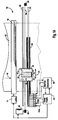
- a printing cartridge 28 is mounted on a carrier 22, which is carried in close proximity to a print receiving media 12, which in turn is transported by roller pairs 16,18. As shown by the arrow 24, the cartridge 28 (and thus the printhead carrier 22) is mounted for orthogonal, reciprocatory motion relative to the print receiving media 12. To this end, and as shown in Fig. 1A, the carrier 22 is mounted for reciprocation along a pair of guide shafts 26,27.
- Cartridge 28 includes a recording head unit, or printhead 29, which includes a chip 20 attached to a nozzle plate 30 having a plurality of individually selectable and actuable nozzles 30a (see Fig.
- the nozzle plate portion 30 is preferably made of stainless steel (sometimes coated on opposite sides with gold and/or tantalum, for attachment to the thick film side) or a hard, thin and high wear resistant polymer layer.
- Nozzle plate 30 is shown in the drawings as being transparent to better view the silicon structure thereunder. A typical nozzle plate implemented in conjunction with the invention, however, would not be transparent.
- Ink ejection nozzles 30a in the nozzle plate 30 of the ink jet printhead 29 confront the print receiving media 12, and ink may be ejected by thermally heating the ink in the nozzles, to effect printing on the print receiving media 12. It should be noted that the nozzles 30a shown in Fig. 2 are not to scale, and while a plurality are shown, the number is only by way of example.
- the reciprocatory or side-to-side motion of the carrier 22 is established by a carrier drive, in the illustrated instance, having a transmission mechanism including a cable or drive belt 34 and pulleys 36,38 which carry the belt 34 driven by a motor 40.
- a carrier drive in the illustrated instance, having a transmission mechanism including a cable or drive belt 34 and pulleys 36,38 which carry the belt 34 driven by a motor 40.
- the print cartridge 28 may be moved and positioned at designated positions along a path defined by and under control of the carrier drive and machine electronics 46.
- the carrier 22 and the cartridge 28 are connected electrically by a flexible printed circuit cable 42 for supplying power from the power supply 44 to cartridge 29, and to supply control and data signals to cartridge 29 from the machine electronics 46, which includes the printer control logic (PCL).
- PCL printer control logic
- the nozzle plate 30 is bonded to chip 20 which in turn is bonded to the reservoir 32.
- the chip I/O including control signals and power, is applied through TAB circuit 31 and spaced apart integrated lands 33 therein (see Figs. 1C, 5 and 6) for making I/O (including electrical) connection to the chip 20.
- the tape 31 extends along one surface of the reservoir 32 with terminal pads 31a (see Fig.
- the electro-thermal converting element associated with each nozzle 30a, is driven selectively in accordance with recording data so that ink droplets eject from the nozzles 30a in the nozzle plate 30 and impinge upon the surface of the print receiving media 12, wherein the ink drops form the recording information on the print receiving media 12.
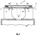
- Fig. 2 is a greatly enlarged, schematic representation of an Integrated Circuit (IC) chip 20, having a bank or cell 21 of electrical components, which forms part of printhead 29.
- IC Integrated Circuit
- chip 20 is approximately 1 / 3 inch (about 8.5mm) by 1/9 inch (about 2.8mm).
- Chip 20 is one of many cut from, in a conventional manner, a silicon wafer which has been coated with photo resist, photo lithographically exposed through a mask, subjected to an etch bath and doped by processes well known in the art of semiconductor manufacturing. The process is repeated through several layers, including metalization for I/O pads 35, usually making multiple integrated circuit chips on a single wafer, which is then cut or diced, into individual chips, or dies.
- cell 21 of chip 20 includes electrical components, such as resistors 23 and active circuits 25a and 25b.
- Resistors 23 are preferably arranged in longitudinally extending arrays, wherein one resistor is associated with each nozzle 30a.
- Each resistor is connected to an active circuit 25a or 25b comprising, for example, a field effect transistor (FET), arranged, as shown in Fig. 2, on opposite sides of the arrays of resistors 23 (shown in Fig. 3).
- the FETs are represented by two columns 25a, 25b.
- the active circuits may be arranged e.g. in a matrix and include data lines and address lines. I/O pads 35, along the periphery of the chip 20, may be connected to an address and data line bus (not shown) in the chip.
- chip 20 includes a via or vias 52 through the silicon to allow the passing of ink from ink reservoir 32 behind the chip into the channels or chambers 54 over the heater resistors 23.
- the vias 52 may be cut by means of grit blasting or laser cutting.
- the channels or chambers 54 may be formed in conjunction with and as defined by the nozzle plate 30 and a thick spacer or insulating film 56.
- the thick film layer 56 may be etched to expose the heater resistor 23, which may include a protective metal over the heater resistors, thus placing the resistors 23 beneath the ink channels.
- the ink channels and nozzles may be created from a single polymer material as known in the art.
- Such a polymer nozzle plate would include slots or openings to expose electrical connection points, such as pads 35.
- the ink flows from the via hole 52 into the channels 54 and out through the nozzles 30a, as illustrated by the arrows.
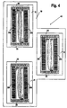
- a single large megachip containing multiple cells or banks 21 is formed in which at least a pair of overlapping, horizontally displaced cells 21 are cut from a single semiconductor wafer.
- elements shown in Figs. 2-8 which are functionally equivalent are identified using common element numbers.
- cell 21 of Fig. 2 is substantially identical to cells 21 of Figs. 4-8.
- Fig. 4 illustrates a partial view of a printhead 48 including a single chip, or megachip 50, having multiple silicon cells or banks 21 which has been extracted from a semiconductor silicon wafer by dicing a single silicon substrate 100 (see Figs. 7 and 8).
- Megachip 50 is covered with a nozzle plate 30, which includes nozzles or orifices 30a for the expulsion of ink.
- Nozzles 30a may be provided by a single nozzle plate covering all the cells or banks 21 of megachip 50, or may be comprised of multiple nozzle plates corresponding to the number of cells 21.
- the cells 21 are substantially identical and correspond generally to cells 21 illustrated in Fig. 2.
- the number of individual cell patterns comprising megachip 50 will depend in part upon the number of heater resistors 23 in each of the individual cells 21. Other considerations for the choice of the number of individual cell patterns include structural strength and yield considerations. A choice of three cell patterns provides more structural strength than two in columnar alignment, but two that are adjacent but columnarly offset with overlap are also stronger than two cells that are aligned in a column. While megachips with additional cells are also possible, and may even be desirable in certain requirements for extremely high resolution, additional cell requirements become expensive due to a concomitant decrease in yield.
- any known silicon technology method may be employed for fabrication of the silicon cells.
- the active circuits (FETs 25a and 25b) and the passive elements (such as the heater resistors 23) may all be formed on each silicon cell 21 on the megachip 50 by typical large scale integrated circuit techniques as is known by those skilled in the art.
- Example manufacturing techniques are taught in U.S. Patent Re 32,572 to Hawkins, et al., and US-A-5,000,811 to Campunelli, et al.
- the TAB circuitry or tape 31 is schematically shown in a position relative to the megachip 50.
- the tape 31 is formed with multiple cutouts or openings to receive megachip 50, with enough space therebetween to permit bonding of the beam ends of lands 33 to selected, individual pads of the pads 35.
- the position of the megachip 50 relative to the tape 31 is shown in dotted or hidden lines.
- the lands 33 in the tape are connected to the terminal pads 31a or, depending upon the ink jet head configuration, may include a cell interconnection scheme depending upon the desire of the machine designer for parallel operation of selected nozzles or independent control of each nozzle.
- the terminal pads 31a are in turn engaged with the protrusion 43 of Fig. 1C of circuit 42 for electrical coupling to machine electronics 46. (See Figs. 1A and 1C).
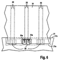
- Fig. 6 is a fragmentary, enlarged, view in plan of a portion of TAB circuitry or tape 31 connected to the chip 21 of Fig 2.
- the extended beam ends 33a of the lands 33 are bonded to individual pads 35 of cell 21.
- the area 21a (bounded by phantom lines) along the edge 21b is conventionally covered by an encapsulant, such as potting compound, to inhibit ink bridging (and therefore shorts) between the beams 33a and the chip I/O pads 35.
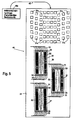
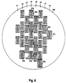
- Fig. 7 is a partial schematic representation of a silicon semiconductor wafer 100 incorporating a layout of multiple banks or cells 21 of heater and active semiconductor matrix arrays.
- the multiple silicon cells 21 are positioned in a line vertically, but are offset horizontally such that, for example, the cells of a first column overlap the space between cells of an adjacent column.
- multiple cells form a megachip and the number of cells can be expanded as desired to form larger arrays.
- the individual cell layout in the wafer has deliberately been expanded to increase spacing at appropriate or selected intervals, and is dependent upon the particular design of a megachip 50 desired.
- the cell layout may be uniform with small row spacing between the cells 21 in the columns c1, c2, c3, ....cn, but with adjacent columns being offset so that the columns of dies are overlapping such that each cell in an adjacent column overlaps two of the cells in its previous adjacent column.
- the columns With a megachip 50 layout or design of three cells 21, such as shown in Fig. 4, the columns may be laid out in the manner illustrated in Fig. 7, or as suggested above, the cell spacing in each column may be uniform, depending upon the megachip 50 design.
- the design requirement simply stated, is based upon the amount of cell or nozzle overlap needed or desired. If the design layout is as shown in Fig. 4, the overlap is about 1/3, i.e. the cell overlap between the cells in adjacent columns of the megachip is approximately 1/3.
- the overlap is only critical to the resolution and coverage desired by the designer. For example, such overlap may result in increased resolution by horizontally interleaving the nozzles associated with a first cell with the nozzles associated with a second cell.
- Fig. 8 shows an array of cell patterns structured such that a laser selective cutting process can be performed.
- the selective cutting process begins with testing and a yield study of the silicon cells 21. Then an optimum arrangement is determined for dicing the cells 21.
- three cell megachips, 50a, 50b are designated or selected (by way of example only) for dicing as by the heavier megachip outline.
- megachip 50c as shown by the heavier megachip outline 51c, includes two cells 21 instead of three.
- the selective cutting process is performed by a laser dicing tool, but other suitable die cutting methods may be employed, as is known in the art.
- the designated number of cells for the megachip may be cut as one unit if the yield is appropriate, or they may be cut into individual chips if an individual cell cannot be grouped with an adjacent cell.
- the alignment or fiducial marks (+ -), as shown for example in Fig. 2, may be employed for proper alignment of the nozzle plates and the individual chips relative to one another.
- Some of the cells 21 may be indicated as "good”, i.e. completely functional and of acceptable quality, in accordance with their initial tests, but an adjacent cell, for example, near the periphery of the wafer 100, may not be of sufficient yield or quality to allow its use in a megachip.
- "good" chips such as chips 50d and 50e, may be extracted and employed in single ink jet printheads for a low end design, or may be mated in overlapping relation (such as the cell pattern of chip 50c) to form a megachip.
- the effective yield of a silicon wafer is improved.
- An advantage of the unitary, or single cutout, multi-cell megachip over separate chips is that the alignment of the silicon cells in the megachip is more precise than a bonding alignment because the silicon cells are processed together on the wafer, and the tolerances involved are predominantly the wafer fabrication tolerances. Thus, precision relative positioning of the heater elements among silicon cells can be accomplished.
- An additional enhancement to this concept may include a wiring connection scheme between single cell patterns, such that common connections are made on the megachip to reduce the total number of off chip connections needed on the TAB bonder. Accordingly, some cell-to-cell wiring on the megachip with the metalization fabrication stages already utilized in the processing of the megachip is possible. In embodiments which include a polymer nozzle plate, slots or openings may be formed therein to expose electrical connection points associated with such cell-to-cell wiring.
- a unitary multiple cell "mega" chip may be achieved.
- Such a megachip is preferably formed near the center of the silicon wafer where yield is high, and increased nozzle resolution per die may be realized. For example, resolution of 1000 or more heaters per chip capacity may be achieved.
- Single cells, or banks, may be formed (or salvaged) on the die near the wafer edges where yields are lower, and such single banks or cells may be employed where very high resolution may not be a prime factor, or may be combined to form megachips.
Landscapes
- Engineering & Computer Science (AREA)
- Manufacturing & Machinery (AREA)
- Physics & Mathematics (AREA)
- General Physics & Mathematics (AREA)
- Particle Formation And Scattering Control In Inkjet Printers (AREA)
Applications Claiming Priority (2)
| Application Number | Priority Date | Filing Date | Title |
|---|---|---|---|
| US08/752,091 US5719605A (en) | 1996-11-20 | 1996-11-20 | Large array heater chips for thermal ink jet printheads |
| US752091 | 2000-12-29 |
Publications (3)
| Publication Number | Publication Date |
|---|---|
| EP0845359A2 true EP0845359A2 (de) | 1998-06-03 |
| EP0845359A3 EP0845359A3 (de) | 1999-03-10 |
| EP0845359B1 EP0845359B1 (de) | 2003-03-12 |
Family
ID=25024841
Family Applications (1)
| Application Number | Title | Priority Date | Filing Date |
|---|---|---|---|
| EP97309382A Expired - Lifetime EP0845359B1 (de) | 1996-11-20 | 1997-11-20 | Heizelementchips für Matrixen mit grossen Abmessungen für thermische Tintenstrahldruckköpfe |
Country Status (5)
| Country | Link |
|---|---|
| US (1) | US5719605A (de) |
| EP (1) | EP0845359B1 (de) |
| JP (1) | JPH10181029A (de) |
| AU (1) | AU715596B2 (de) |
| DE (1) | DE69719683T2 (de) |
Cited By (1)
| Publication number | Priority date | Publication date | Assignee | Title |
|---|---|---|---|---|
| WO2002074545A1 (en) * | 2001-03-21 | 2002-09-26 | Olivetti I-Jet S.P.A. | Substrate for a thermal ink jet printhead, a colour printhead in particular, and ink jet printhead incorporation this substrate |
Families Citing this family (49)
| Publication number | Priority date | Publication date | Assignee | Title |
|---|---|---|---|---|
| US6190931B1 (en) * | 1997-07-15 | 2001-02-20 | Silverbrook Research Pty. Ltd. | Method of manufacture of a linear spring electromagnetic grill ink jet printer |
| US6110754A (en) * | 1997-07-15 | 2000-08-29 | Silverbrook Research Pty Ltd | Method of manufacture of a thermal elastic rotary impeller ink jet print head |
| US6350013B1 (en) | 1997-10-28 | 2002-02-26 | Hewlett-Packard Company | Carrier positioning for wide-array inkjet printhead assembly |
| US6164762A (en) * | 1998-06-19 | 2000-12-26 | Lexmark International, Inc. | Heater chip module and process for making same |
| ITTO980592A1 (it) * | 1998-07-06 | 2000-01-06 | Olivetti Lexikon Spa | Testina di stampa a getto di inchiostro con piastrina di silicio di grandi dimensioni e relativo processo di fabbricazione |
| KR100325526B1 (ko) | 1998-10-26 | 2002-04-17 | 윤종용 | 잉크 분사 장치의 제조 방법 |
| US6705705B2 (en) * | 1998-12-17 | 2004-03-16 | Hewlett-Packard Development Company, L.P. | Substrate for fluid ejection devices |
| US6341845B1 (en) | 2000-08-25 | 2002-01-29 | Hewlett-Packard Company | Electrical connection for wide-array inkjet printhead assembly with hybrid carrier for printhead dies |
| US6450614B1 (en) | 1998-12-17 | 2002-09-17 | Hewlett-Packard Company | Printhead die alignment for wide-array inkjet printhead assembly |
| US6464333B1 (en) | 1998-12-17 | 2002-10-15 | Hewlett-Packard Company | Inkjet printhead assembly with hybrid carrier for printhead dies |
| US6428145B1 (en) | 1998-12-17 | 2002-08-06 | Hewlett-Packard Company | Wide-array inkjet printhead assembly with internal electrical routing system |
| US6213587B1 (en) | 1999-07-19 | 2001-04-10 | Lexmark International, Inc. | Ink jet printhead having improved reliability |
| US6427597B1 (en) | 2000-01-27 | 2002-08-06 | Patrice M. Aurenty | Method of controlling image resolution on a substrate |
| JP2001260366A (ja) * | 2000-03-21 | 2001-09-25 | Nec Corp | インクジェット記録ヘッドおよびその製造方法 |
| US6543880B1 (en) | 2000-08-25 | 2003-04-08 | Hewlett-Packard Company | Inkjet printhead assembly having planarized mounting layer for printhead dies |
| KR100406943B1 (ko) * | 2000-10-28 | 2003-11-21 | 삼성전자주식회사 | 프린트 어레이 헤드 및 그 제조방법 |
| DE60204485T2 (de) * | 2001-01-05 | 2006-03-16 | Hewlett-Packard Development Co., L.P., Houston | Integrierter programmierbarer Auslösepulsgenerator für Tintenstrahldruckkopf |
| US6585339B2 (en) | 2001-01-05 | 2003-07-01 | Hewlett Packard Co | Module manager for wide-array inkjet printhead assembly |
| US6726298B2 (en) | 2001-02-08 | 2004-04-27 | Hewlett-Packard Development Company, L.P. | Low voltage differential signaling communication in inkjet printhead assembly |
| US6409307B1 (en) | 2001-02-14 | 2002-06-25 | Hewlett-Packard Company | Coplanar mounting of printhead dies for wide-array inkjet printhead assembly |
| US6557976B2 (en) * | 2001-02-14 | 2003-05-06 | Hewlett-Packard Development Company, L.P. | Electrical circuit for wide-array inkjet printhead assembly |
| US6394580B1 (en) | 2001-03-20 | 2002-05-28 | Hewlett-Packard Company | Electrical interconnection for wide-array inkjet printhead assembly |
| US6431683B1 (en) | 2001-03-20 | 2002-08-13 | Hewlett-Packard Company | Hybrid carrier for wide-array inkjet printhead assembly |
| US6428141B1 (en) * | 2001-04-23 | 2002-08-06 | Hewlett-Packard Company | Reference datums for inkjet printhead assembly |
| US6619786B2 (en) * | 2001-06-08 | 2003-09-16 | Lexmark International, Inc. | Tab circuit for ink jet printer cartridges |
| US6852241B2 (en) * | 2001-08-14 | 2005-02-08 | Lexmark International, Inc. | Method for making ink jet printheads |
| US6679581B2 (en) | 2001-10-25 | 2004-01-20 | Hewlett-Packard Development Company, L.P. | Surface deformation of carrier for printhead dies |
| US6575559B2 (en) | 2001-10-31 | 2003-06-10 | Hewlett-Packard Development Company, L.P. | Joining of different materials of carrier for fluid ejection devices |
| US6935727B2 (en) * | 2001-12-18 | 2005-08-30 | Agilent Technologies, Inc. | Pulse jet print head assembly having multiple reservoirs and methods for use in the manufacture of biopolymeric arrays |
| US20030113730A1 (en) * | 2001-12-18 | 2003-06-19 | Daquino Lawrence J. | Pulse jet print head having multiple printhead dies and methods for use in the manufacture of biopolymeric arrays |
| US6726300B2 (en) * | 2002-04-29 | 2004-04-27 | Hewlett-Packard Development Company, L.P. | Fire pulses in a fluid ejection device |
| KR100428793B1 (ko) * | 2002-06-26 | 2004-04-28 | 삼성전자주식회사 | 잉크젯 프린터 헤드 및 그 제조 방법 |
| CN101521254B (zh) * | 2003-02-07 | 2011-06-01 | 三洋电机株式会社 | 半导体元件及其制造方法 |
| US7372077B2 (en) * | 2003-02-07 | 2008-05-13 | Sanyo Electric Co., Ltd. | Semiconductor device |
| US6736488B1 (en) | 2003-05-23 | 2004-05-18 | Hewlett-Packard Development Company, L.P. | Electrical interconnect for printhead assembly |
| US7621625B2 (en) * | 2005-03-31 | 2009-11-24 | Heidelberger Druckmaschinen Ag | Ink jet device with individual shut-off |
| JP2006315306A (ja) * | 2005-05-13 | 2006-11-24 | Sony Corp | 液体吐出ヘッドの製造方法、液体吐出ヘッド及び液体吐出装置 |
| US7549736B2 (en) * | 2006-06-29 | 2009-06-23 | Lexmark International, Inc. | Printhead assembly having ink flow channels to accommodate offset chips |
| WO2010063744A1 (en) * | 2008-12-02 | 2010-06-10 | Oce-Technologies B.V. | Method of manufacturing an ink jet print head |
| US8118405B2 (en) * | 2008-12-18 | 2012-02-21 | Eastman Kodak Company | Buttable printhead module and pagewide printhead |
| US20100154190A1 (en) * | 2008-12-19 | 2010-06-24 | Sanger Kurt M | Method of making a composite device |
| KR20100082216A (ko) * | 2009-01-08 | 2010-07-16 | 삼성전자주식회사 | 잉크젯 헤드 칩 및 이를 채용한 잉크젯 프린트 헤드 |
| JP5196086B2 (ja) * | 2011-02-09 | 2013-05-15 | 大日本印刷株式会社 | 金めっき層を有するステンレス基板とステンレス基板への部分金めっきパターンの形成方法 |
| US9446587B2 (en) * | 2013-02-28 | 2016-09-20 | Hewlett-Packard Development Company, L.P. | Molded printhead |
| EP2961612B1 (de) | 2013-02-28 | 2019-08-07 | Hewlett-Packard Development Company, L.P. | Formung einer fluidströmungsstruktur |
| BR112015020862B1 (pt) | 2013-02-28 | 2021-05-25 | Hewlett-Packard Development Company, L.P. | barra de impressão moldada |
| US9724920B2 (en) | 2013-03-20 | 2017-08-08 | Hewlett-Packard Development Company, L.P. | Molded die slivers with exposed front and back surfaces |
| US9808812B2 (en) | 2014-06-20 | 2017-11-07 | The Procter & Gamble Company | Microfluidic delivery system |
| US9434165B2 (en) | 2014-08-28 | 2016-09-06 | Funai Electric Co., Ltd. | Chip layout to enable multiple heater chip vertical resolutions |
Family Cites Families (20)
| Publication number | Priority date | Publication date | Assignee | Title |
|---|---|---|---|---|
| US3842491A (en) * | 1972-12-08 | 1974-10-22 | Ibm | Manufacture of assorted types of lsi devices on same wafer |
| US4047184A (en) * | 1976-01-28 | 1977-09-06 | International Business Machines Corporation | Charge electrode array and combination for ink jet printing and method of manufacture |
| JPS58107633A (ja) * | 1981-12-21 | 1983-06-27 | Canon Inc | 特殊チツプを逃げたシヨツト配列方法 |
| US4472875A (en) * | 1983-06-27 | 1984-09-25 | Teletype Corporation | Method for manufacturing an integrated circuit device |
| US4812859A (en) * | 1987-09-17 | 1989-03-14 | Hewlett-Packard Company | Multi-chamber ink jet recording head for color use |
| US4829324A (en) * | 1987-12-23 | 1989-05-09 | Xerox Corporation | Large array thermal ink jet printhead |
| US4851371A (en) * | 1988-12-05 | 1989-07-25 | Xerox Corporation | Fabricating process for large array semiconductive devices |
| US5041190A (en) * | 1990-05-16 | 1991-08-20 | Xerox Corporation | Method of fabricating channel plates and ink jet printheads containing channel plates |
| US5057854A (en) * | 1990-06-26 | 1991-10-15 | Xerox Corporation | Modular partial bars and full width array printheads fabricated from modular partial bars |
| JP2902506B2 (ja) * | 1990-08-24 | 1999-06-07 | キヤノン株式会社 | 半導体装置の製造方法及び半導体装置 |
| US5160945A (en) * | 1991-05-10 | 1992-11-03 | Xerox Corporation | Pagewidth thermal ink jet printhead |
| US5160403A (en) * | 1991-08-09 | 1992-11-03 | Xerox Corporation | Precision diced aligning surfaces for devices such as ink jet printheads |
| US5218754A (en) * | 1991-11-08 | 1993-06-15 | Xerox Corporation | Method of manufacturing page wide thermal ink-jet heads |
| US5278584A (en) * | 1992-04-02 | 1994-01-11 | Hewlett-Packard Company | Ink delivery system for an inkjet printhead |
| US5648806A (en) * | 1992-04-02 | 1997-07-15 | Hewlett-Packard Company | Stable substrate structure for a wide swath nozzle array in a high resolution inkjet printer |
| US5504507A (en) * | 1992-10-08 | 1996-04-02 | Xerox Corporation | Electronically readable performance data on a thermal ink jet printhead chip |
| US5410340A (en) * | 1993-11-22 | 1995-04-25 | Xerox Corporation | Off center heaters for thermal ink jet printheads |
| US5680702A (en) * | 1994-09-19 | 1997-10-28 | Fuji Xerox Co., Ltd. | Method for manufacturing ink jet heads |
| EP0709740A1 (de) * | 1994-09-30 | 1996-05-01 | Texas Instruments Incorporated | Integrierte Schaltung und Verfahren zur Herstellung derselben |
| EP0771272A1 (de) * | 1995-04-12 | 1997-05-07 | Eastman Kodak Company | Monolithische druckköpfe und verfahren zu deren herstellung |
-
1996
- 1996-11-20 US US08/752,091 patent/US5719605A/en not_active Expired - Lifetime
-
1997
- 1997-10-21 AU AU42809/97A patent/AU715596B2/en not_active Ceased
- 1997-11-20 DE DE69719683T patent/DE69719683T2/de not_active Expired - Fee Related
- 1997-11-20 JP JP9336339A patent/JPH10181029A/ja not_active Withdrawn
- 1997-11-20 EP EP97309382A patent/EP0845359B1/de not_active Expired - Lifetime
Cited By (2)
| Publication number | Priority date | Publication date | Assignee | Title |
|---|---|---|---|---|
| WO2002074545A1 (en) * | 2001-03-21 | 2002-09-26 | Olivetti I-Jet S.P.A. | Substrate for a thermal ink jet printhead, a colour printhead in particular, and ink jet printhead incorporation this substrate |
| US7008047B2 (en) | 2001-03-21 | 2006-03-07 | Olivetti I-Jet S.P.A. | Substrate for a thermal ink jet printhead, a colour printhead in particular, and ink jet printhead incorporation this substrate |
Also Published As
| Publication number | Publication date |
|---|---|
| DE69719683T2 (de) | 2003-10-16 |
| EP0845359A3 (de) | 1999-03-10 |
| MX9708937A (es) | 1998-05-31 |
| AU715596B2 (en) | 2000-02-03 |
| EP0845359B1 (de) | 2003-03-12 |
| US5719605A (en) | 1998-02-17 |
| DE69719683D1 (de) | 2003-04-17 |
| JPH10181029A (ja) | 1998-07-07 |
| AU4280997A (en) | 1998-05-28 |
Similar Documents
| Publication | Publication Date | Title |
|---|---|---|
| EP0845359B1 (de) | Heizelementchips für Matrixen mit grossen Abmessungen für thermische Tintenstrahldruckköpfe | |
| US4985710A (en) | Buttable subunits for pagewidth "Roofshooter" printheads | |
| EP0705694B1 (de) | Drucksystem | |
| US5192959A (en) | Alignment of pagewidth bars | |
| US6705705B2 (en) | Substrate for fluid ejection devices | |
| JP3268937B2 (ja) | インクジェット記録ヘッド用基板及びそれを用いたヘッド | |
| JP4006256B2 (ja) | 記録ヘッド、および、それを備える記録装置 | |
| CA2084344C (en) | Structure and method for aligning a substrate with respect to orifices in an inkjet printhead | |
| US5434607A (en) | Attachment of nozzle plate to flexible circuit for facilitating assembly of printhead | |
| US5563642A (en) | Inkjet printhead architecture for high speed ink firing chamber refill | |
| EP0705705A2 (de) | Tintenstrahldruckpatrone | |
| EP0705695A2 (de) | Tintenzuführsystem | |
| EP0646462B1 (de) | Zum Eliminieren von Tintenbahnfehlern ausgebildeter Tintenstrahldruckkopf | |
| EP0705706A2 (de) | Tintenstrahldrucksystem | |
| KR20070011360A (ko) | 유체 방출 장치 | |
| EP0970812B1 (de) | Tintentrahldruckkopf mit grossem Silizium-wafer und zugehöriges Herstellungsverfahren | |
| US5410340A (en) | Off center heaters for thermal ink jet printheads | |
| JPH11216872A (ja) | インクジェット式プリントヘッドの製造方法 | |
| US6137506A (en) | Ink jet recording head with a plurality of orifice plates | |
| MXPA97008937A (en) | Large systems of chips heaters for impression heads of ink jet | |
| JP2006502023A (ja) | 並行インクジェット印刷装置とその製造方法 | |
| JPH0858101A (ja) | インクジェット記録ヘッド及びこれを搭載するインクジェット記録装置 | |
| JPH06171087A (ja) | インクジェット記録ヘッド |
Legal Events
| Date | Code | Title | Description |
|---|---|---|---|
| PUAI | Public reference made under article 153(3) epc to a published international application that has entered the european phase |
Free format text: ORIGINAL CODE: 0009012 |
|
| AK | Designated contracting states |
Kind code of ref document: A2 Designated state(s): DE FR GB |
|
| AX | Request for extension of the european patent |
Free format text: AL;LT;LV;MK;RO;SI |
|
| PUAL | Search report despatched |
Free format text: ORIGINAL CODE: 0009013 |
|
| AK | Designated contracting states |
Kind code of ref document: A3 Designated state(s): AT BE CH DE DK ES FI FR GB GR IE IT LI LU MC NL PT SE |
|
| AX | Request for extension of the european patent |
Free format text: AL;LT;LV;MK;RO;SI |
|
| 17P | Request for examination filed |
Effective date: 19990331 |
|
| AKX | Designation fees paid |
Free format text: DE FR GB |
|
| 17Q | First examination report despatched |
Effective date: 20010219 |
|
| GRAG | Despatch of communication of intention to grant |
Free format text: ORIGINAL CODE: EPIDOS AGRA |
|
| GRAG | Despatch of communication of intention to grant |
Free format text: ORIGINAL CODE: EPIDOS AGRA |
|
| GRAH | Despatch of communication of intention to grant a patent |
Free format text: ORIGINAL CODE: EPIDOS IGRA |
|
| GRAH | Despatch of communication of intention to grant a patent |
Free format text: ORIGINAL CODE: EPIDOS IGRA |
|
| GRAA | (expected) grant |
Free format text: ORIGINAL CODE: 0009210 |
|
| AK | Designated contracting states |
Designated state(s): DE FR GB |
|
| REG | Reference to a national code |
Ref country code: GB Ref legal event code: FG4D |
|
| REF | Corresponds to: |
Ref document number: 69719683 Country of ref document: DE Date of ref document: 20030417 Kind code of ref document: P |
|
| ET | Fr: translation filed | ||
| PLBE | No opposition filed within time limit |
Free format text: ORIGINAL CODE: 0009261 |
|
| STAA | Information on the status of an ep patent application or granted ep patent |
Free format text: STATUS: NO OPPOSITION FILED WITHIN TIME LIMIT |
|
| 26N | No opposition filed |
Effective date: 20031215 |
|
| PGFP | Annual fee paid to national office [announced via postgrant information from national office to epo] |
Ref country code: FR Payment date: 20081117 Year of fee payment: 12 |
|
| PGFP | Annual fee paid to national office [announced via postgrant information from national office to epo] |
Ref country code: DE Payment date: 20081223 Year of fee payment: 12 |
|
| PGFP | Annual fee paid to national office [announced via postgrant information from national office to epo] |
Ref country code: GB Payment date: 20081128 Year of fee payment: 12 |
|
| GBPC | Gb: european patent ceased through non-payment of renewal fee |
Effective date: 20091120 |
|
| REG | Reference to a national code |
Ref country code: FR Ref legal event code: ST Effective date: 20100730 |
|
| PG25 | Lapsed in a contracting state [announced via postgrant information from national office to epo] |
Ref country code: FR Free format text: LAPSE BECAUSE OF NON-PAYMENT OF DUE FEES Effective date: 20091130 |
|
| PG25 | Lapsed in a contracting state [announced via postgrant information from national office to epo] |
Ref country code: DE Free format text: LAPSE BECAUSE OF NON-PAYMENT OF DUE FEES Effective date: 20100601 |
|
| PG25 | Lapsed in a contracting state [announced via postgrant information from national office to epo] |
Ref country code: GB Free format text: LAPSE BECAUSE OF NON-PAYMENT OF DUE FEES Effective date: 20091120 |