EP0844720A2 - Verfahren und Vorrichtung zur Stromüberwachung für Halbleiterschaltungen - Google Patents
Verfahren und Vorrichtung zur Stromüberwachung für Halbleiterschaltungen Download PDFInfo
- Publication number
- EP0844720A2 EP0844720A2 EP97115865A EP97115865A EP0844720A2 EP 0844720 A2 EP0844720 A2 EP 0844720A2 EP 97115865 A EP97115865 A EP 97115865A EP 97115865 A EP97115865 A EP 97115865A EP 0844720 A2 EP0844720 A2 EP 0844720A2
- Authority
- EP
- European Patent Office
- Prior art keywords
- voltage
- switch
- ufp
- bot
- voltages
- Prior art date
- Legal status (The legal status is an assumption and is not a legal conclusion. Google has not performed a legal analysis and makes no representation as to the accuracy of the status listed.)
- Granted
Links
Images

Classifications
-
- H—ELECTRICITY
- H03—ELECTRONIC CIRCUITRY
- H03K—PULSE TECHNIQUE
- H03K17/00—Electronic switching or gating, i.e. not by contact-making and –breaking
- H03K17/08—Modifications for protecting switching circuit against overcurrent or overvoltage
- H03K17/082—Modifications for protecting switching circuit against overcurrent or overvoltage by feedback from the output to the control circuit
- H03K17/0822—Modifications for protecting switching circuit against overcurrent or overvoltage by feedback from the output to the control circuit in field-effect transistor switches
-
- H—ELECTRICITY
- H02—GENERATION; CONVERSION OR DISTRIBUTION OF ELECTRIC POWER
- H02H—EMERGENCY PROTECTIVE CIRCUIT ARRANGEMENTS
- H02H7/00—Emergency protective circuit arrangements specially adapted for specific types of electric machines or apparatus or for sectionalised protection of cable or line systems, and effecting automatic switching in the event of an undesired change from normal working conditions
- H02H7/10—Emergency protective circuit arrangements specially adapted for specific types of electric machines or apparatus or for sectionalised protection of cable or line systems, and effecting automatic switching in the event of an undesired change from normal working conditions for converters; for rectifiers
- H02H7/12—Emergency protective circuit arrangements specially adapted for specific types of electric machines or apparatus or for sectionalised protection of cable or line systems, and effecting automatic switching in the event of an undesired change from normal working conditions for converters; for rectifiers for static converters or rectifiers
- H02H7/122—Emergency protective circuit arrangements specially adapted for specific types of electric machines or apparatus or for sectionalised protection of cable or line systems, and effecting automatic switching in the event of an undesired change from normal working conditions for converters; for rectifiers for static converters or rectifiers for inverters, i.e. DC/AC converters
- H02H7/1227—Emergency protective circuit arrangements specially adapted for specific types of electric machines or apparatus or for sectionalised protection of cable or line systems, and effecting automatic switching in the event of an undesired change from normal working conditions for converters; for rectifiers for static converters or rectifiers for inverters, i.e. DC/AC converters responsive to abnormalities in the output circuit, e.g. short circuit
-
- H—ELECTRICITY
- H02—GENERATION; CONVERSION OR DISTRIBUTION OF ELECTRIC POWER
- H02P—CONTROL OR REGULATION OF ELECTRIC MOTORS, ELECTRIC GENERATORS OR DYNAMO-ELECTRIC CONVERTERS; CONTROLLING TRANSFORMERS, REACTORS OR CHOKE COILS
- H02P7/00—Arrangements for regulating or controlling the speed or torque of electric DC motors
- H02P7/03—Arrangements for regulating or controlling the speed or torque of electric DC motors for controlling the direction of rotation of DC motors
- H02P7/04—Arrangements for regulating or controlling the speed or torque of electric DC motors for controlling the direction of rotation of DC motors by means of a H-bridge circuit
-
- H—ELECTRICITY
- H02—GENERATION; CONVERSION OR DISTRIBUTION OF ELECTRIC POWER
- H02H—EMERGENCY PROTECTIVE CIRCUIT ARRANGEMENTS
- H02H7/00—Emergency protective circuit arrangements specially adapted for specific types of electric machines or apparatus or for sectionalised protection of cable or line systems, and effecting automatic switching in the event of an undesired change from normal working conditions
- H02H7/08—Emergency protective circuit arrangements specially adapted for specific types of electric machines or apparatus or for sectionalised protection of cable or line systems, and effecting automatic switching in the event of an undesired change from normal working conditions for dynamo-electric motors
- H02H7/0833—Emergency protective circuit arrangements specially adapted for specific types of electric machines or apparatus or for sectionalised protection of cable or line systems, and effecting automatic switching in the event of an undesired change from normal working conditions for dynamo-electric motors for electric motors with control arrangements
- H02H7/0838—Emergency protective circuit arrangements specially adapted for specific types of electric machines or apparatus or for sectionalised protection of cable or line systems, and effecting automatic switching in the event of an undesired change from normal working conditions for dynamo-electric motors for electric motors with control arrangements with H-bridge circuit
Definitions
- the invention describes a method and one for implementing this method necessary device for current monitoring for semiconductor components in circuit arrangements, especially for power semiconductor components according to the characteristics of Preamble of claim 1.
- Current monitors, in particular for overcurrent monitoring, are known several times from the literature by describing their arrangements.
- the state-of-the-art drivers for half-bridge and full-bridge circuits work with the voltage drop via specially provided shunt resistors. This is particularly uneconomical for high-performance switches because it is suitable for this Resistors are expensive and the power dissipation that occurs must be dissipated, which the Performance of the circuit arrangement is restricted and its efficiency deteriorates.
- Fig. 1 shows the state of the circuit technology.
- the control circuit of a single circuit breaker with integrated short-circuit monitoring is shown in the block diagram.
- Fig. 1 shows part of the context of the entirety of all parallel or series connected circuit breakers of the same Ant and in the same way represents only the part of the control of the overall circuit arrangement which is decisive for the invention.
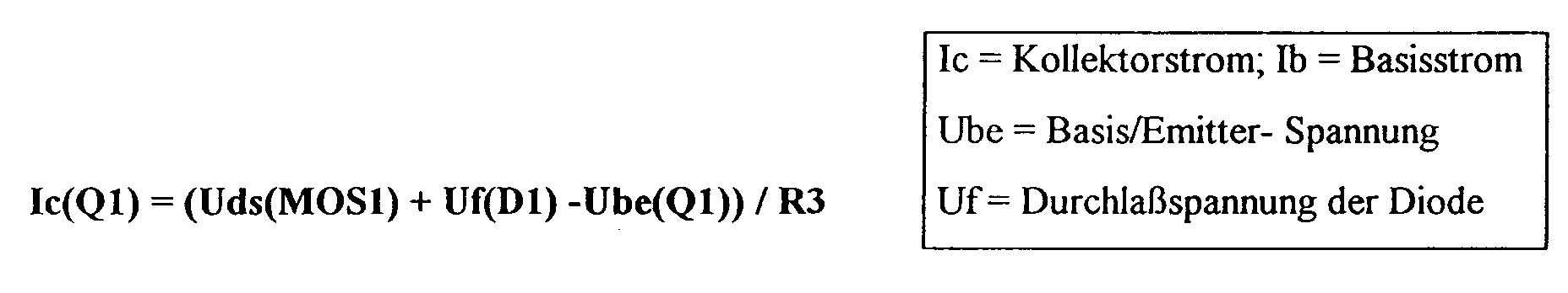
- the operating current of the MOSFET (MOS1) shown as an example is monitored by measuring the voltage drop across the series resistor (Rshunt). This voltage drop is proportional to the current flow across the circuit breaker (MOS1). Vz provides the DC power supply (for example a battery via a DC link) and Rlast represent the working resistance (e.g. motor drive).
- Rshunt series resistor
- Vz provides the DC power supply (for example a battery via a DC link)
- Rlast represent the working resistance (e.g. motor drive).
- the present invention has set itself the task of a method and its Realization of a simple and inexpensive device for recording and transmitting the Introduce operating current values for short-circuit monitoring of a circuit arrangement.
- Fig. 2 shows a schematic diagram of an operating current monitoring by Uds detection.
- Vz represents the power supply via an intermediate circuit. If an IGBT is used, Uce detection is analogous. The relationship between current flow and voltage drop is determined by the output characteristic of the power semiconductor component used.
- the driver is one Control electronics overlaid.
- the driver must be one of these higher-level control electronics Report any overcurrent that has occurred in the form of a resulting error signal to be able to react electronically accordingly.
- complex structures such as half or Full bridge circuits, the circuitry required is considerable since there are several Drivers are used and in each driver a monitoring circuit for the Forward voltage of the downstream semiconductor switch with appropriate logic and a signal line to the control electronics must be provided for each driver.
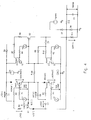
- FIG. 3 shows a basic circuit diagram of an entire full-bridge circuit with Uds detection according to the prior art, as is also found in the catalog SEMIDRIVER "from SEMIKRON from 1/95 on page 2 can be seen in the block diagram.
- MOS 1 to MOS 4 The transmission of a possible error signal of the drivers in the BOTTOM position can be done very simply, since they have the same reference potential as the control electronics.
- the reference potential of the drivers in the TOP position is at the source potential of the Switching transistors in TOP position and jumps to DC link level (Vz) with every switching operation.
- the monitoring circuit in the driver must then also jump with this potential.
- the transmission of an error signal from the jumping TOP reference voltage potential is complex to the resting potential of the overlaid control electronics of the one outlined here Microcontrollers. This is usually done inductively via signal transformations or through optocouplers.
- the TOP driver stage can be powered by DC / DC converters or bootstrap switching.
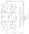
- Fig. 4 outlines the inventive solution of Uds monitoring using the example of an entire full bridge with circuit breakers.
- four power switches (MOS1 to MOS4) are connected together in the arrangement.
- the power supply comes from the intermediate circuit (Vz), the pulse voltage sources (V1 to V4) are representative of the driver output stages (two in TOP and two in BOTTOM position).
- V1 applies a control voltage Ugsan MOS1, this controls after reaching Switch-on threshold through. At this point, a current flows into the resistor (R3) Diode (D1) in the forward direction and via the resistor (R3) in the emitter of the Transistor (Q1).
- the collector current (Ic from Q1) is calculated as follows:
- a Uds measurement is only carried out when the power transistor is switched on and by checking The entire full bridge is monitored with a single voltage.
- this can inventive circuit arrangement also applied in half-bridges and individual switches will.
- a circuit corresponding to the prior art is used to filter such interference Derivation of Vsense from U (R11) required. According to the invention, this is made from only one only in Fig. 4 exemplarily shown clamp and filter circuit for interference suppression entire full bridge formed, it consists of the resistor R12, the diodes D7 and D8, the capacitance C1 and the voltage source Vlimit.
- the inventive solution can also be used to detect the Switching currents are used.
- the relationship between current flow (drain or Collector current) and the voltage drop (drain-source or collector-emitter voltage) is in many semiconductor devices from the control voltage and the Temperature affected.
- the voltage drop across the switched-on MOSFET Uf depends on its drain current, its control voltage Ugs and the crystal temperature (Temp.).
- the control voltage Ugs is specified by the driver and is therefore known. By Detect the temperature of the semiconductor switch, which is recommended anyway and off Operational safety reasons should happen, it is possible to keep the actual current flow over the drain-source section when using MOSFET or collector-emitter section Use of IGBT.
- the compensation of the temperature influence on the voltage drop over the Semiconductor switch can be done by a simple analog network or by the example here applied microcontroller.
- the inventive solution can Monitoring circuit can be implemented in a very cost-effective manner.
Landscapes
- Engineering & Computer Science (AREA)
- Power Engineering (AREA)
- Power Conversion In General (AREA)
- Electronic Switches (AREA)
- Protection Of Static Devices (AREA)
Abstract
Description
- Fig. 2
- zeigt eine Prinzipskizze der Betriebstromüberwachung durch Uds- Erfassung nach dem Stand der Technik.
- Fig. 3
- zeigt ein Prinzipschaltbild einer gesamten Vollbrückenschaltung mit Uds- Erfassung nach dem Stand der Technik.
- Fig. 4
- stellt die erfinderische Lösung der Uds- Überwachung einer gesamten Leistungsschalter-Vollbrücke dar.
Claims (10)
- Verfahren zur Stromüberwachung für Halbleiterschalter, die in Halb- oder Vollbrücken vorzugsweise in Schaltungsanordnungen der Leistungselektronik, bestehend aus Schaltern in TOP- und BOTTOM- Positionen, insbesondere bei Einsatz von MOSFET- oder IGBT- Schaltern,
dadurch gekennzeichnet, daß
durch Wandlung der Flußspannungen Uftop aller Halbleiterschalter in TOP- Position in von diesen Flußspannungen abgeleitete Ströme Ifptop und anschließende Rückwandlung dieser Ströme Ifptop in Spannungen Ufptop auf der BOTTOM- Bezugsspannungs- Potentialebene GND und analoge Disjunktion dieser Spannungen Ufptop mit den von den Flußspannungen der BOTTOM- Schalter Ufbot abgeleiteten Spannungen Ufpbot, so daß das analoge Disjunktionsprodukt eine Spannung U(R11) ergibt, die wiederum von der Flußspannung desjenigen Halbleiterschalters abgeleitet ist, der die höchste Flußspannung in der zu überwachenden Anordnung aufweist. - Verfahren nach Anspruch 1, dadurch gekennzeichnet, daß
die Wandlung der Flußspannung Uftop eines Halbleiters in TOP- Position in einen von dieser Flußspannung abgeleiteten Strom Ifptop und Rückwandlung dieses Stromes in eine Spannung Ufptop auf der BOTTOM- Bezugsspannungs- Potentialebene durchgeführt wird. - Verfahren nach Anspruch 1, dadurch gekennzeichnet, daß
auf der Grundlage des proportionalen Verhaltens von Ufptop zu Uftop und Ufpbot zu Ufbot unter Berücksichtigung von Steuerspannung und Kristalltemperatur der Halbleiterschalter sowie Auswertung von U(R11) der maximale Schalterstrom in der zu überwachenden Anordnung ermittelt wird. - Verfahren nach Ansprüche 1 oder 2, dadurch gekennzeichnet, daß
die Wandlung der Flußspannung Uftop des jeweiligen TOP- Schalters in einen dazu proportionalen Strom Ifptop durch das Steuersignal dieses TOP- Schalters gelenkt wird, so daß der Strom Ifptop ausschließlich ein Abbild des Spannungsabfalles über diesem TOP- Schalter in dessen eingeschaltetem Zustand ist. - Verfahren nach Ansprüche 1 oder 2, dadurch gekennzeichnet, daß
die Ableitung von Ufpbot aus der Flußspannung Ufbot des jeweiligen Halbleiterschalters in BOTTOM- Position (MOS2 bzw. MOS4) durch das Steuersignal dieses BOTTOM- Schalters gelenkt wird, so daß die Spannung Ufpbot ein Abbild des Spannungsabfalles über diesem BOTTOM- Schalter ausschließlich in dessen eingeschaltetem Zustand ist. - Vorrichtung zur Durchführung des Verfahrens nach vorgenannten Ansprüchen, dadurch gekennzeichnet, daß
die Schaltstruktur für die Wandlung der Flußspannung Uftop in Ifptop des entsprechenden Halbleiterschalters MOS1 (bzw. MOS3) in TOP- Position eine Diode D1 (bzw. D4) aufweist, die im Sperrzustand des jeweiligen TOP- Schalters die im allgemeinen vergleichsweise hohe Sperrspannung über diesem TOP- Schalter von der Wandelstruktur trennt. - Vorrichtung zur Durchführung des Verfahrens nach vorgenannten Verfahrensansprüchen, dadurch gekennzeichnet, daß
die Schaltstruktur für die Wandlung der Flußspannungen Uftop in Ifptop der entsprechenden TOP- Schalter MOS1 (bzw. MOS3) einen Transistor Q1 (bzw. Q2) mit einem äußeren Emitterwiderstand R3 (bzw. R8) aufweist, der so verschalten ist, daß der Spannungsabfall über seiner Steuerstrecke die Flußspannung von D1 (bzw. D4) kompensiert und der Spannungsabfall über den entsprechenden äußeren Emitterwiderstand R3 (bzw. R8) gleich der Flußspannung über diesem TOP- Schalter MOS1 (bzw. MOS3) ist. - Vorrichtung nach Anspruch 7, dadurch gekennzeichnet, daß
der Transistor Q1 (bzw. Q2) den in dem Widerstand R3 (bzw. R8) fließenden Strom Ifptop aufgrund seines Stromquellencharakters weitgehend unabhängig vom Source- Potential des TOP- Schalters MOS1 (bzw. MOS3) in einen Bürdenwiderstand (R11) einprägt, so daß der Spannungsabfall an diesem Bürdenwiderstand proportional zur Flußspannung dieses TOP- Schalters MOS1 (bzw. MOS3) ist. - Vorrichtung zur Durchführung des Verfahrens nach vorgenannten Verfahrensansprüchen, dadurch gekennzeichnet, daß
die Schaltstruktur für die Ableitung der Spannung Ufpbot aus Ufbot, die ein Abbild der Flußspannung des entsprechenden Leistungsschalters in BOTTOM- Position ist, eine Diode D2 (bzw. D5) aufweist, die im Sperrzustand des BOTTOM- Schalters MOS2 (bzw. MOS4) die im allgemeinen hohe Sperrspannung über diesem Halbleiterschalter abtrennt. - Vorrichtung zur Durchführung des Verfahrens nach vorgenannten Verfahrensansprüchen, dadurch gekennzeichnet, daß
die Schaltstruktur für die Ableitung der Spannung Ufpbot aus Ufbot, die ein Abbild der Flußspannung des Leistungsschalters in BOTTOM- Position ist, eine Diode D3 (bzw. D6) enthält, welche die Flußspannung von D2 (bzw. D5) kompensiert, gleichzeitig dient die Diode D3 (bzw. D5) der analogen Disjunktion der von den Flußspannungen der Leistungsschalter in TOP- Position abgeleiteten Spannungen Ufptop mit den Flußspannungen der Leistungsschalter in BOTTOM- Position abgeleiteten Spannungen.
Applications Claiming Priority (2)
| Application Number | Priority Date | Filing Date | Title |
|---|---|---|---|
| DE19648562 | 1996-11-23 | ||
| DE19648562A DE19648562C2 (de) | 1996-11-23 | 1996-11-23 | Verfahren und Vorrichtung zur Stromüberwachung für Halbleiterschaltungen |
Publications (3)
| Publication Number | Publication Date |
|---|---|
| EP0844720A2 true EP0844720A2 (de) | 1998-05-27 |
| EP0844720A3 EP0844720A3 (de) | 1999-08-18 |
| EP0844720B1 EP0844720B1 (de) | 2002-04-17 |
Family
ID=7812575
Family Applications (1)
| Application Number | Title | Priority Date | Filing Date |
|---|---|---|---|
| EP97115865A Expired - Lifetime EP0844720B1 (de) | 1996-11-23 | 1997-09-12 | Verfahren und Vorrichtung zur Stromüberwachung für Halbleiterschaltungen |
Country Status (2)
| Country | Link |
|---|---|
| EP (1) | EP0844720B1 (de) |
| DE (1) | DE19648562C2 (de) |
Cited By (3)
| Publication number | Priority date | Publication date | Assignee | Title |
|---|---|---|---|---|
| WO2005078887A1 (de) * | 2004-02-14 | 2005-08-25 | Conti Temic Microelectronic Gmbh | Schaltungsanordnung zum überlastungsschutz eines ansteuerbaren schaltelements |
| DE102004037543A1 (de) * | 2004-08-03 | 2006-03-16 | Infineon Technologies Ag | Vorrichtung zum Schutz einer Halbbrückenschaltungsanordnung vor einem Kurzschluss über einer Last |
| WO2012107010A1 (de) * | 2011-02-07 | 2012-08-16 | Infineon Technologies Austria Ag | Verfahren zur ansteuerung eines transistors und ansteuerschaltung |
Families Citing this family (8)
| Publication number | Priority date | Publication date | Assignee | Title |
|---|---|---|---|---|
| DE29909206U1 (de) | 1999-05-28 | 2000-10-05 | Ellenberger & Poensgen | Schutzeinrichtung |
| DE10121970B4 (de) * | 2001-05-05 | 2004-05-27 | Semikron Elektronik Gmbh | Leistungshalbleitermodul in Druckkontaktierung |
| DE10213648B4 (de) * | 2002-03-27 | 2011-12-15 | Semikron Elektronik Gmbh & Co. Kg | Leistungshalbleitermodul |
| DE10248644B4 (de) | 2002-10-18 | 2008-07-03 | Semikron Elektronik Gmbh & Co. Kg | Leistungshalbleitermodul |
| DE10249568B4 (de) * | 2002-10-24 | 2015-05-07 | Robert Bosch Gmbh | Fehleranalyse einer Wechselrichter-Schaltung |
| DE102013100452A1 (de) * | 2013-01-17 | 2014-07-31 | Zf Lenksysteme Gmbh | Verfahren zum betreiben einer elektrischen maschine |
| DE102019219160A1 (de) * | 2019-12-09 | 2021-06-10 | Zf Friedrichshafen Ag | Sicherer Betrieb eines elektrischen Verbrauchers |
| DE102021214350A1 (de) | 2021-12-15 | 2023-06-15 | Robert Bosch Gesellschaft mit beschränkter Haftung | Detektion von Kurzschlussströmen in stromgeregelten Endstufen |
Family Cites Families (5)
| Publication number | Priority date | Publication date | Assignee | Title |
|---|---|---|---|---|
| IT1220186B (it) * | 1987-11-02 | 1990-06-06 | Sgs Microelettronica Spa | Mutliplex analogico per la rivelazione dell'ampiezza e della direzione della corrente in stadi a ponte utilizzando un'unica resistenza di revelazione |
| US4924158A (en) * | 1989-04-03 | 1990-05-08 | General Motors Corporation | Motor driver protection circuit |
| JPH06209592A (ja) * | 1992-11-03 | 1994-07-26 | Texas Instr Deutschland Gmbh | 誘導性負荷を給電する回路構成 |
| JP3052648B2 (ja) * | 1993-02-21 | 2000-06-19 | 日産自動車株式会社 | 半導体装置 |
| US5444591A (en) * | 1993-04-01 | 1995-08-22 | International Rectifier Corporation | IGBT fault current limiting circuit |
-
1996
- 1996-11-23 DE DE19648562A patent/DE19648562C2/de not_active Expired - Fee Related
-
1997
- 1997-09-12 EP EP97115865A patent/EP0844720B1/de not_active Expired - Lifetime
Cited By (5)
| Publication number | Priority date | Publication date | Assignee | Title |
|---|---|---|---|---|
| WO2005078887A1 (de) * | 2004-02-14 | 2005-08-25 | Conti Temic Microelectronic Gmbh | Schaltungsanordnung zum überlastungsschutz eines ansteuerbaren schaltelements |
| DE102004037543A1 (de) * | 2004-08-03 | 2006-03-16 | Infineon Technologies Ag | Vorrichtung zum Schutz einer Halbbrückenschaltungsanordnung vor einem Kurzschluss über einer Last |
| DE102004037543B4 (de) * | 2004-08-03 | 2017-02-16 | Infineon Technologies Ag | Vorrichtung zum Schutz einer Halbbrückenschaltungsanordnung vor einem Kurzschluss über einer Last |
| WO2012107010A1 (de) * | 2011-02-07 | 2012-08-16 | Infineon Technologies Austria Ag | Verfahren zur ansteuerung eines transistors und ansteuerschaltung |
| US9093836B2 (en) | 2011-02-07 | 2015-07-28 | Infineon Technologies Austria Ag | Method for controlling a transistor and control circuit |
Also Published As
| Publication number | Publication date |
|---|---|
| DE19648562C2 (de) | 2001-02-15 |
| DE19648562A1 (de) | 1998-06-04 |
| EP0844720B1 (de) | 2002-04-17 |
| EP0844720A3 (de) | 1999-08-18 |
Similar Documents
| Publication | Publication Date | Title |
|---|---|---|
| DE69122419T2 (de) | Schutzschaltung für eine Halbleiteranordnung | |
| EP0665634B1 (de) | Schaltungsanordnung mit einem Feldeffekttransistor | |
| DE69508644T2 (de) | Halbleiter-Leistungsmodul und -Leistungswandlervorrichtung | |
| DE19548612B4 (de) | Mehrkreisiges Fahrzeugbordnetz mit einem elektronischen Analogschalter | |
| DE2638178A1 (de) | Schutzvorrichtung fuer elektronische schaltungen gegen ueberspannungen | |
| DE19600807A1 (de) | Intelligentes, getrenntes Halbbrückenleistungsmodul | |
| EP0075656B2 (de) | Elektronische Überstromschutzvorrichtung | |
| EP0268930B1 (de) | Schaltungsanordnung eines sich selbst schützenden Leistungsschalters | |
| EP0844720B1 (de) | Verfahren und Vorrichtung zur Stromüberwachung für Halbleiterschaltungen | |
| DE19743346C2 (de) | Schaltungsanordnung zur getakteten Stromregelung von induktiven Lasten | |
| EP0387729B1 (de) | Elektronische Schützansteuerung | |
| EP0790699A2 (de) | Verfahren zum Ansteuern eines Gleichstrommotors und Vorrichtung zur Durchführung dieses Verfahrens | |
| EP0255067B1 (de) | Schaltungsanordnung zur Strombegrenzung | |
| DE3741394A1 (de) | Schaltungsanordnung zum schutz vor verpolungsschaeden fuer lastkreise mit einem mos-fet als schalttransistor | |
| EP0201878A2 (de) | Schaltungsanordnung mit einem p-schaltenden n-Kanal MOS-Transistor | |
| DE4037348C1 (en) | Protective circuitry for power semiconductor switches - uses bridging voltage clamping circuit consisting of diode and Zener diode belonging to rectifier pair | |
| EP3491738B1 (de) | Verfahren und vorrichtung zur ansteuerung eines halbleiterschalters | |
| DE3930896A1 (de) | Verpolschutzschaltung | |
| EP0560086B1 (de) | Schutzschaltung für einen Leistungs-MOSFET, der eine induktive Last treibt | |
| EP0891039A2 (de) | Kapazitives Netzteil | |
| DE10317374A1 (de) | Steuerschaltung für Leistungsvorrichtung | |
| DE19620034C2 (de) | Schaltnetzgerät | |
| DE3515133A1 (de) | Kurzschlussfeste transistorendstufe | |
| EP0696849A2 (de) | Steuergerät mit einer Schaltungsanordnung zum Schutz des Steuergerätes bei Unterbrechung der Steuergerätemasse | |
| DE2851956A1 (de) | Schaltungsanordnung zur elektronischen sicherungsueberwachung |
Legal Events
| Date | Code | Title | Description |
|---|---|---|---|
| PUAI | Public reference made under article 153(3) epc to a published international application that has entered the european phase |
Free format text: ORIGINAL CODE: 0009012 |
|
| AK | Designated contracting states |
Kind code of ref document: A2 Designated state(s): FR GB IT |
|
| PUAL | Search report despatched |
Free format text: ORIGINAL CODE: 0009013 |
|
| AK | Designated contracting states |
Kind code of ref document: A3 Designated state(s): AT BE CH DE DK ES FI FR GB GR IE IT LI LU MC NL PT SE |
|
| 17P | Request for examination filed |
Effective date: 19990712 |
|
| AKX | Designation fees paid |
Free format text: FR GB IT |
|
| REG | Reference to a national code |
Ref country code: DE Ref legal event code: 8566 |
|
| 17Q | First examination report despatched |
Effective date: 20000808 |
|
| GRAG | Despatch of communication of intention to grant |
Free format text: ORIGINAL CODE: EPIDOS AGRA |
|
| GRAG | Despatch of communication of intention to grant |
Free format text: ORIGINAL CODE: EPIDOS AGRA |
|
| GRAH | Despatch of communication of intention to grant a patent |
Free format text: ORIGINAL CODE: EPIDOS IGRA |
|
| GRAH | Despatch of communication of intention to grant a patent |
Free format text: ORIGINAL CODE: EPIDOS IGRA |
|
| REG | Reference to a national code |
Ref country code: GB Ref legal event code: IF02 |
|
| GRAA | (expected) grant |
Free format text: ORIGINAL CODE: 0009210 |
|
| AK | Designated contracting states |
Kind code of ref document: B1 Designated state(s): FR GB IT |
|
| GBT | Gb: translation of ep patent filed (gb section 77(6)(a)/1977) |
Effective date: 20020709 |
|
| ET | Fr: translation filed | ||
| PLBE | No opposition filed within time limit |
Free format text: ORIGINAL CODE: 0009261 |
|
| STAA | Information on the status of an ep patent application or granted ep patent |
Free format text: STATUS: NO OPPOSITION FILED WITHIN TIME LIMIT |
|
| 26N | No opposition filed |
Effective date: 20030120 |
|
| REG | Reference to a national code |
Ref country code: GB Ref legal event code: 732E |
|
| REG | Reference to a national code |
Ref country code: FR Ref legal event code: TP Ref country code: FR Ref legal event code: CD |
|
| PGFP | Annual fee paid to national office [announced via postgrant information from national office to epo] |
Ref country code: FR Payment date: 20110721 Year of fee payment: 15 |
|
| PGFP | Annual fee paid to national office [announced via postgrant information from national office to epo] |
Ref country code: IT Payment date: 20110923 Year of fee payment: 15 |
|
| PGFP | Annual fee paid to national office [announced via postgrant information from national office to epo] |
Ref country code: GB Payment date: 20120808 Year of fee payment: 16 |
|
| REG | Reference to a national code |
Ref country code: FR Ref legal event code: ST Effective date: 20130531 |
|
| PG25 | Lapsed in a contracting state [announced via postgrant information from national office to epo] |
Ref country code: FR Free format text: LAPSE BECAUSE OF NON-PAYMENT OF DUE FEES Effective date: 20121001 Ref country code: IT Free format text: LAPSE BECAUSE OF NON-PAYMENT OF DUE FEES Effective date: 20120912 |
|
| GBPC | Gb: european patent ceased through non-payment of renewal fee |
Effective date: 20130912 |
|
| PG25 | Lapsed in a contracting state [announced via postgrant information from national office to epo] |
Ref country code: GB Free format text: LAPSE BECAUSE OF NON-PAYMENT OF DUE FEES Effective date: 20130912 |