EP0842004B1 - Cutting tool - Google Patents
Cutting tool Download PDFInfo
- Publication number
- EP0842004B1 EP0842004B1 EP96913965A EP96913965A EP0842004B1 EP 0842004 B1 EP0842004 B1 EP 0842004B1 EP 96913965 A EP96913965 A EP 96913965A EP 96913965 A EP96913965 A EP 96913965A EP 0842004 B1 EP0842004 B1 EP 0842004B1
- Authority
- EP
- European Patent Office
- Prior art keywords
- cutting tool
- substrate
- coated
- coating
- coated cutting
- Prior art date
- Legal status (The legal status is an assumption and is not a legal conclusion. Google has not performed a legal analysis and makes no representation as to the accuracy of the status listed.)
- Expired - Lifetime
Links
Images

Classifications
-
- B—PERFORMING OPERATIONS; TRANSPORTING
- B23—MACHINE TOOLS; METAL-WORKING NOT OTHERWISE PROVIDED FOR
- B23B—TURNING; BORING
- B23B27/00—Tools for turning or boring machines; Tools of a similar kind in general; Accessories therefor
- B23B27/14—Cutting tools of which the bits or tips or cutting inserts are of special material
- B23B27/141—Specially shaped plate-like cutting inserts, i.e. length greater or equal to width, width greater than or equal to thickness
- B23B27/145—Specially shaped plate-like cutting inserts, i.e. length greater or equal to width, width greater than or equal to thickness characterised by having a special shape
- B23B27/146—Means to improve the adhesion between the substrate and the coating
-
- B—PERFORMING OPERATIONS; TRANSPORTING
- B23—MACHINE TOOLS; METAL-WORKING NOT OTHERWISE PROVIDED FOR
- B23B—TURNING; BORING
- B23B2228/00—Properties of materials of tools or workpieces, materials of tools or workpieces applied in a specific manner
- B23B2228/08—Properties of materials of tools or workpieces, materials of tools or workpieces applied in a specific manner applied by physical vapour deposition [PVD]
-
- B—PERFORMING OPERATIONS; TRANSPORTING
- B23—MACHINE TOOLS; METAL-WORKING NOT OTHERWISE PROVIDED FOR
- B23B—TURNING; BORING
- B23B2260/00—Details of constructional elements
- B23B2260/072—Grooves
-
- Y—GENERAL TAGGING OF NEW TECHNOLOGICAL DEVELOPMENTS; GENERAL TAGGING OF CROSS-SECTIONAL TECHNOLOGIES SPANNING OVER SEVERAL SECTIONS OF THE IPC; TECHNICAL SUBJECTS COVERED BY FORMER USPC CROSS-REFERENCE ART COLLECTIONS [XRACs] AND DIGESTS
- Y10—TECHNICAL SUBJECTS COVERED BY FORMER USPC
- Y10T—TECHNICAL SUBJECTS COVERED BY FORMER US CLASSIFICATION
- Y10T407/00—Cutters, for shaping
- Y10T407/24—Cutters, for shaping with chip breaker, guide or deflector
-
- Y—GENERAL TAGGING OF NEW TECHNOLOGICAL DEVELOPMENTS; GENERAL TAGGING OF CROSS-SECTIONAL TECHNOLOGIES SPANNING OVER SEVERAL SECTIONS OF THE IPC; TECHNICAL SUBJECTS COVERED BY FORMER USPC CROSS-REFERENCE ART COLLECTIONS [XRACs] AND DIGESTS
- Y10—TECHNICAL SUBJECTS COVERED BY FORMER USPC
- Y10T—TECHNICAL SUBJECTS COVERED BY FORMER US CLASSIFICATION
- Y10T407/00—Cutters, for shaping
- Y10T407/27—Cutters, for shaping comprising tool of specific chemical composition
-
- Y—GENERAL TAGGING OF NEW TECHNOLOGICAL DEVELOPMENTS; GENERAL TAGGING OF CROSS-SECTIONAL TECHNOLOGIES SPANNING OVER SEVERAL SECTIONS OF THE IPC; TECHNICAL SUBJECTS COVERED BY FORMER USPC CROSS-REFERENCE ART COLLECTIONS [XRACs] AND DIGESTS
- Y10—TECHNICAL SUBJECTS COVERED BY FORMER USPC
- Y10T—TECHNICAL SUBJECTS COVERED BY FORMER US CLASSIFICATION
- Y10T408/00—Cutting by use of rotating axially moving tool
- Y10T408/78—Tool of specific diverse material
-
- Y—GENERAL TAGGING OF NEW TECHNOLOGICAL DEVELOPMENTS; GENERAL TAGGING OF CROSS-SECTIONAL TECHNOLOGIES SPANNING OVER SEVERAL SECTIONS OF THE IPC; TECHNICAL SUBJECTS COVERED BY FORMER USPC CROSS-REFERENCE ART COLLECTIONS [XRACs] AND DIGESTS
- Y10—TECHNICAL SUBJECTS COVERED BY FORMER USPC
- Y10T—TECHNICAL SUBJECTS COVERED BY FORMER US CLASSIFICATION
- Y10T408/00—Cutting by use of rotating axially moving tool
- Y10T408/81—Tool having crystalline cutting edge
Definitions
- the present invention relates to a coated cutting tool according to the preamble of claim 1 and as known for example from US-A-5 075.181.
- the invention pertains to a cutting tool, that provides for improved chip control, improved surface finishing properties, and/or improved coating adhesion.
- the invention further pertains to a coated cutting tool with a low cobalt substrate and having a long tool life.
- the invention pertains to a cutting tool, and a method of making the same, with a rake face having microtopographical properties that provide chip control features without the need for a structural chip breaker. More specifically, the rake surface of the cutting tool has an appropriate surface roughness so as to provide chip control properties.
- the invention concerns a cutting tool, and a method of making the same, that has the capability to machine the workpiece so as to present a smooth machined surface. More particularly, the invention concerns a cutting tool with a flank face that is smooth so as to produce a desirably smooth surface finish on the surface of the workpiece.
- the invention pertains to a cutting tool, and a method of making the same, having a coating scheme thereon, such as, for example, a single layer coating deposited by physical vapor deposition (PVD) or a multi-layer coating wherein at least one layer is deposited by PVD, wherein the coating has improved adhesion.
- a coating scheme thereon such as, for example, a single layer coating deposited by physical vapor deposition (PVD) or a multi-layer coating wherein at least one layer is deposited by PVD, wherein the coating has improved adhesion.
- Certain machining operations such as, for example, threading, grooving or cutoff, have the tendency to produce long chip strings or "birds nests". The production of these long chip strings, as opposed to shorter C-shaped/figure six-shaped chips or short coils, are not desirable.
- Certain materials are difficult to machine without creating long chip strings. In other words, due to the very nature of the material there is the tendency to produce long chip strings through any machining operation on these materials. These materials include titanium alloys, aluminum alloys and low carbon steels.
- U.S. Patent No. 4,710,069 to Loquist illustrates a cutting tool that provides a structural chip breaker in the form of a number of depressions that cooperate with the chip breaking face.
- PVD physical vapor deposition
- the thickness could not exceed about 5 micrometers and still maintain adequate adherence to the substrate for cutting tool applications. Because of the high residual stresses associated with the application of a PVD-applied TiC or cubic Boron Nitride coating, such a coating has not been able to applied at any functional thickness, i.e., a thickness that is sufficient for the cutting tool to be commercially practical, with adequate adhesion strength.
- multi-layer coating schemes applied by a combination of chemical vapor deposition (CVD) and PVD techniques.
- CVD chemical vapor deposition
- PVD physical vapor deposition
- One such example of a multi-layer coating scheme comprises a base layer of TiN applied by CVD, an intermediate layer of TiCN applied by CVD, and a top layer of TiN applied by PVD techniques to a substrate that has binder enrichment in a surface layer.
- This combination coating scheme is a subject of U.S. Patent No. 5,250,367 to Santhanam et al. entitled BINDER ENRICHED CVD AND PVD COATED CUTTING TOOL, and assigned to the assignee of the present patent application.
- the substrate has a bulk cobalt content of 3 to 12 weight percent with 5 to 8 weight percent and 5.5 to 7 weight percent as more preferable ranges for the cobalt content. Specific examples include cobalt contents of 10.5, 8.5 and 9.5 weight percent cobalt.
- the cobalt has a range of 3 to 12 weight percent with more preferable ranges of 5 to 7 weight percent and 5.7 to 6.3 weight percent.
- the specific examples show cobalt contents of 6.0, 8.5, 9.75, 10, 10.5 and 11.5 weight percent.
- the binder (cobalt) ranges between 5 and 15 weight cobalt with more preferable ranges being between 7 and 13 weight percent and 8 and 12 weight percent cobalt.
- U.S. Patent No. 5,066,553 to Yoshimura entitled SURFACE-COATED TOOL MEMBER OF TUNGSTEN CARBIDE BASED CEMENTED CARBIDE mentions the resintering of a substrate to achieve better adherence for a CVD applied coating.
- a cutting tool By providing such a cutting tool, one can reduce the costs of manufacture by lowering the cost of manufacturing the rams that form the powder material into the shape of the cutting tool.
- Such a cutting tool can also lower the cost of manufacture by decreasing the number of rams that the manufacturer must keep in inventory.
- Such a cutting tool will also reduce the costs associated with selling and distributing cutting tools due to the reduction in the number of cutting tools that the user must keep in inventory.
- an improved cutting tool that has a PVD coating that exhibits improved adherence to the substrate, that has thicker PVD coatings, and that permits the use of new adherent PVD-applied coatings such as, for example, TiC, aluminum oxide, and cubic boron nitride.
- the present invention is directed to a coated cutting tool having a substrate presenting a surface wherein the surface includes a rake face and flank face with the rake face and the flank face intersecting to form a cutting edge, and a PVD coating on at least a portion of the surface of the substrate, for example, as disclosed in US-Patent No. 5,075,181, which is considered to be the closest prior art.
- the coated cutting tool according to the invention is characterized in that the portion of the substrate surface which is coated has a surface roughness between about 15 microinches R a and about 125 microinches R a ; and the PVD coating has an adherence as measured by the Rockwell A indentation adhesion load test of greater than or equal to 60 kg.
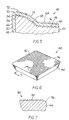
- FIGS. 1 and 2 illustrate a first specific embodiment of the cutting tool of the invention generally designated as 20.
- Cutting tool 20 includes a substrate 22 which has a rake face 24 and a flank face 26.
- the cutting tool substrate may also be made in any of the standard shapes and sizes such as those identified in the American National Standard for Cutting Tools - Indexable Inserts - Identification System, ANSI B212.4-1986. Inserts may also have various chipbreaker structures (not shown) on their rake face as well to facilitate breakage and removal of chips.
- the substrate 22 can be selected from many possible substrate materials suitable for use as a cutting tool substrate.
- Basic material categories includes tool steels, cemented carbides, cermets, ceramics, ceramic composites, polycrystalline diamond, and polycrystalline cubic Boron Nitride as candidates for a cutting tool substrate.
- one substrate is a cobalt cemented tungsten carbide composition.
- the cobalt ranges between about .2 weight percent to about 20 weight percent with the balance consisting essentially of tungsten carbide, and optionally, carbides and carbonitrides with tungsten, titanium, tantalum, zirconium, hafnium and/or niobium.
- cermets In the category of cermets there are titanium carbonitride-based materials having a cobalt and/or nickel binder metal. These cermets include the following grades of cermets sold by Kennametal Inc. of Latrobe, Pennsylvania (assignee of the present patent application): KT125, KT150, KT175, and KT195.
- ceramics there are silicon nitride-based, or aluminum oxide-based, ceramics with or without reinforcement additives such as silicon carbide and titanium carbide in whisker or particulate form.
- whisker reinforced ceramics In the category of ceramic composites there are whisker reinforced ceramics. Examples of these types of composites includes silicon carbide whiskers and/or titanium carbide whiskers in an alumina matrix.
- a coating 28 covers the rake face 24 and the flank face 26 of the substrate 22.
- the use of a coating 28 may or may not be necessary depending upon the specific application and the specific substrate of the cutting tool. In those cases where coatings are used, there are many variations for a coating scheme.
- a single or multi-layer coating may be applied by physical vapor deposition techniques.
- One such example is a coating of TiAIN or TiN applied by PVD.
- One example of a multi-layer coating is a TiN-TiCN-TiN coating scheme such as that mentioned in U.S. Patent No. 5,250,367 to Santhanam et al. which discloses coating schemes that comprise a combination of CVD and PVD techniques or U.S. Patent 5,075,181 to Quinto et al. which discloses a multi-layer coating scheme applied solely by PVD techniques.
- coating layers may be used for cutting tools include the carbides, nitrides, carbonitrides and borides of zirconium, titanium, hafnium and their alloys, alumina, cubic Boron Nitride, silicon nitride, and a thin film polycrystalline diamond layer.
- the rake face 24 of the substrate 22 consists of a microscopically rough surface.
- the peripheral edge 30 of the substrate 22 is at the joinder of the rake face 24 and the flank face 26.
- the flank face 26 presents a relatively smooth surface.
- coating 28 is illustrated in the first specific embodiment (FIG. 2) as a single layer.
- the coating 28 overlies the substrate 22 so that the complete coated cutting tool 20 presents an exposed rake face 34 and an exposed flank face 36.
- the exposed rake face 34 has a microscopically rough surface.
- the exposed flank face 36 presents a relatively smooth surface as compared to the rake face.
- the exposed peripheral edge 38 is at the juncture of the rake face 34 and flank face 36.
- the roughness of the rough rake surface 24 for the substrate 22, and for the exposed rake face 34 range between 15 microinches R a and 125 microinches R a as measured on a Sheffield Proficorder Spectre Unit.
- a preferable range for this surface roughness is between 25 microinches R a and 125 microinches R a .
- An even more preferable range is between 40 microinches R a and 80 microinches R a .
- the roughness of the exposed smooth flank face 36 is less than 25 microinches R a as measured on a Sheffield Proficorder Spectre Unit.
- a more preferable surface roughness is less than 15 microinches R a .
- the specific embodiment of the cutting tool of FIGS. 1 and 2 presents the advantage of good adhesion of the coating on the rake face of the substrate due to the surface roughness of the rake face of the substrate.
- This cutting tool has good chip control due to the surface roughness on the coated rake face.
- This specific embodiment also exhibits good workpiece surface finish characteristics due to the smooth surface of the coated flank face.
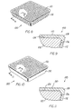
- Cutting tool 42 includes a substrate 44 (see FIG. 5) that presents a rake face 46 and a flank face 48.
- a coating 50 overlies the rake face 46 and the flank face 48.
- the types of substrates and coatings available for cutting tool 42 are the same as those available for cutting tool 20.
- the substrate 44 includes a peripheral edge 54 which is at the joinder of the rake face 46 and the flank face 48.
- the substrate 44 has a peripheral rough surface portion 56, i.e., a portion of the surface that is microscopically rough, which extends inwardly from the peripheral edge 54 of the substrate 44.
- a structural chip breaker 58 which has a microscopically rough surface, extends inwardly from the inward edge of the peripheral rough surface portion 56.
- the substrate 44 further includes a microscopically rough central surface portion 60.
- Central surface portion 60 is bounded by the structural chip breaker 58.
- the coating 50 (see FIG. 5) overlies the substrate 44 to form the coated cutting tool 42 that has an exposed rake face 64 and an exposed flank face 66.
- the coating 50 has a peripheral edge 70 at the joinder of the exposed rake face 64 and the exposed flank face 66 of the coated cutting tool 42.
- an exposed peripheral microscopically rough exposed rake face portion 72 that extends inwardly from the peripheral edge 70.
- An exposed structural chip breaker 74 then extends inwardly from the peripheral microscopically rough exposed rake face portion 72.
- Structural chip breaker 74 has a microscopically rough surface.
- the exposed rake face 64 further includes a central portion 76 that presents a rough surface.
- the cutting insert 42 contains a central hole 78.
- the roughness of the rake surface portions (56, 58, 60) of the substrate and of the exposed rake face portions (72, 74, 76) are the same as described above for rough rake surface 24.
- the roughness of the flank 48 surface of the substrate 22 and the exposed flank face is the same as described above for the smooth flank face 36.
- the central portion 76 of the rake face may have a relatively smooth surface.
- FIGS. 3 through 5 presents a cutting tool that has good adhesion of the coating to the rake face of the substrate because of the surface roughness of the rake face of the substrate.
- This cutting tool has good chip control properties due to the surface roughness of the coated rake face of the cutting tool.
- This cutting tool presents good workpiece surface finishing properties due to the smooth surface of the coated flank face.
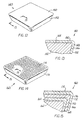
- the uncoated cutting tool 90 can be made from any cutting tool material suitable for use in an uncoated condition.
- the uncoated cutting tool 90 includes a rake face 92 and a flank face 94.
- the rake face 92 presents a microscopically rough surface.
- the peripheral edge 96 is at the joinder of the rake face 92 and the flank face 94.
- the roughness of the rough rake face 92 is the same as that described above for rough rake surface 24.
- the roughness of the flank surface 94 is the same as that described above for the smooth flank face 36.
- the uncoated cutting tool of FIGS. 6 and 7 exhibits good chip control properties due to the rough surface of the rake face of the cutting tool and provides smooth workpiece finishes due to the smooth flank surfaces of the cutting tool.
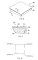
- Cutting tool 100 has a substrate 102 with a rake face 104 and a flank face 106.
- the rake face 104 is rough, i.e., has a rough surface microtopography.
- the flank face 106 of the substrate also has a rough microtopography.
- Cutting tool 100 includes a coating 108 that overlies the surfaces of the substrate 102.
- the rake face 110 of the coated cutting tool has a rough microtopography and the flank face 112 of the coated cutting tool also has a rough microtopography.
- the surface roughness of the coated rake and flank faces (110, 112) is the same as described above for the rough rake surface 24.
- the specific cutting tool of FIGS. 8 and 9 exhibits good coating adherence to the rake and flank faces due to the rake and flank faces of the substrate having a surface roughness.
- This cutting tool provides good chip control properties due to the surface roughness of the coated rake face, but somewhat rougher workpiece surface finishes due to the surface roughness of the coated flank faces.
- Cutting tool 120 has a substrate 122 with a rake face 124 and a flank face 126.
- the rake face 124 is rough, i.e., has a rough surface microtopography.
- the flank face 126 also has a rough microtopography.
- Cutting tool 100 includes a coating 128 that overlies the surfaces of the substrate 122.
- the rake face 130 of the coated cutting tool has a rough microtopography.
- the surface roughness of the rake and flank faces (124, 126) of the substrate 122 and the coated rake face 130 are the same as that described above for the rough rake surface 24.
- the flank face 132 of the coated cutting tool has a smooth microtopography.
- the flank face had to be subjected to a polishing or other treatment to smooth the surface. This is especially true in light of the fact that the flank face of the substrate has a rough microtopography.
- the surface roughness of the coated flank face 132 is the same as described above for the smooth flank face 36.
- the cutting tool of FIGS. 10 and 11 provides the advantage of good coating adherence to the rake and flank faces of the substrate due to the surface roughness of the rake and flank faces of the substrate. This cutting tool also exhibits good chip control due to the surface roughness of the coated rake face. The cutting tool further provides good workpiece surface finish characteristics due to the smoothness of the surface of the coated flank face.
- Cutting tool 140 has a substrate 142 with a rake face 144 and a flank face 146.
- the rake face 144 is rough, i.e., has a rough surface microtopography.
- the flank face 126 has a smooth microtopography.
- Cutting tool 140 includes a coating 148 that overlies the surfaces of the substrate 142.
- the rake face 150 of the coated cutting tool has a smooth microtopography.
- the flank face 152 of the coated cutting tool also has a smooth microtopography. To achieve the smooth microtopography on the rake face of the coated tool, the rake face had to be subjected to a polishing or other treatment to smooth the surface. This is especially true in light of the fact that the rake surface of the substrate has a rough microtopography.
- the surface roughness of the rake face 144 of the substrate is the same as described above for rough rake surface 24.
- the surface roughness of the flank face 146 of the substrate and the coated rake and flank faces (150, 152) is the same as described above for the smooth flank face 36.
- the cutting tool of FIGS. 12 and 13 provides good adherence of the coating to the rake face of the substrate due to the surface roughness of the rake face of the substrate. This cutting tool provides for good workpiece surface finishing properties due to the smooth surface of the coated flank face. This cutting tool also provides for reduced tendency for a built-up edge on the coated rake face due to the surface smoothness of the rake face of the coated cutting tool.
- Cutting tool 160 has a substrate 162 with a rake face 164 and a flank face 166.
- the rake face 164 is rough, i.e., has a rough surface microtopography.
- the flank face 166 has a smooth microtopography.
- Cutting tool 160 includes a multi-layered coating that overlies the surfaces of the substrate 162.
- the coating comprises a base layer 168, an intermediate layer 170, and a top layer 172.
- the rake face 174 of the coated cutting tool has a rough microtopography.
- the flank face 172 of the coated cutting tool has a smooth microtopography.
- the surface roughness of the rake face 164 of the substrate and the coated rake face 174 is the same as described above for rough rake surface 24.
- the surface roughness of the rake face 166 of the substrate and the coated flank face 176 is the same as described above for the smooth flank face 36.
- the cutting tool of FIGS. 14 and 15 exhibits good coating adherence to the rake surface of the substrate due to the surface roughness of the rake face of the substrate, as well as the surface roughness of the overlying coating layers.
- This cutting tool exhibits good chip control properties due to the surface roughness of the exposed coated rake face.
- the cutting tool has good workpiece surface finishing properties due to the surface smoothness of the coated flank face.
- Cutting tool 180 has a substrate 182 with a rake face 184 and a flank face 186.
- the rake face 184 is rough, i.e., has a rough surface microtopography.
- the flank face 186 also has a rough microtopography.
- the surface roughness of the rake and flank faces (184, 186) of the substrate 182 is the same as that described above for the rough rake surface 24.
- Cutting tool 180 includes a coating 188 that overlies the surfaces of the substrate 182.
- the rake face 190 of the coated cutting tool has a smooth microtopography.
- the flank face 192 of the coated cutting tool also has a smooth microtopography. To achieve the smooth microtopography on the rake and flank faces of the coated tool, these faces had to be subjected to a polishing or other treatment to smooth the surface thereof. This is especially true in light of the fact that the rake surface and flank surface of the substrate has a rough microtopography.
- the surface roughness of the coated rake and flank faces (190, 192) is the same as described for the smooth flank face 36.
- the cutting tool of FIGS. 16 and 17 has good coating adhesion to the rake and flank surfaces of the substrate due to the rough rake and flank surfaces of the substrate. This cutting tool has a reduced tendency for a built-up edge on the coated rake face due to the surface smoothness of the coated rake face. This cutting tool provides a good workpiece surface finish due to the surface smoothness of the coated flank face of the cutting tool.
- the basic substrate is preferably made by conventional powder metallurgical techniques. More specifically, the powder components of the substrate are blended and pressed into a green compact. The green compact is then subsequently heat treated, such as by sintering, so as to form a substantially fully dense substrate (in the case of a coated cutting tool) or the uncoated cutting tool.
- a powder blend can be formed into a substantially fully dense body by the simultaneous application of heat and pressure such as, for example, by hot pressing.
- One variation of the sintering process of making the substantially fully dense substrate is to use a ram that forms the powder into the green compact which will form the necessary surface roughness in the green compact.
- a ram that forms the powder into the green compact which will form the necessary surface roughness in the green compact.
- the surface roughness of the as-sintered (or substantially fully dense) tool is excessive, only the undesirably rough locations of the tool may be ground, polished, laser glazed, or otherwise finished to produce the necessary level of smoothness.
- This necessary level of smoothness may, in the case of the flank face, be sufficient to generate a smooth workpiece finish in cutting, yet still leave the rough rake surface of the tool intact to produce the desired chip-flow control.
- the level of smoothness may be sufficient to reduce the tendency for a built-up edge on the rake face.
- the flank surface of the substrate may be in a rough condition so as to improve the coating adhesion on the flank surface of the substrate.
- the tool may be used as-is in the above described condition.
- the tool may be used in an uncoated condition. More commonly, however, this tool will serve as a substrate for a protective wear-resistant coating applied by CVD or PVD methods and then used in the cutting application.
- the coating process parameters as known to those skilled in the art are such that the roughness characteristic of the rake and flank surfaces of the tool may be unchanged from that of the substrate prior to the coating operation.
- the surface roughness of the coated tool is a function of the roughness of the underlying substrate surface and the thickness of the deposited coating.
- the surface roughness of the coating also tends to increase regardless of the underlying surface roughness of the substrate. This could result in the exposed coated surfaces somewhat rougher than the surfaces of the substrate, however, such an increase in surface roughness of the rake surface of the substrate is not deleterious to the desirable chip control properties.
- the increase in surface roughness of the substrate does not negatively impact on the adhesion of the coating to the substrate, but will typically improve the adhesion.
- An increase in the surface roughness of the coated rake surface may generate a problem of a built up edge, i.e., material from the chip is welded to the rake surface of the cutting tool.
- a post coating operation such as polishing, buffing, or laser glazing all or some of the rake surfaces of the tool may be required to smooth the surface of the coating to an acceptable surface smoothness, thus, reducing the potential for the occurrence of a built up edge.
- the built-up edge is a problem that is workpiece material dependent. While smoothing the rake surface reduces chip control properties, it still leaves the coating with good adhesion due to the surface roughness of the rake face of the substrate.
- Still another variation on the basic process uses an additional resintering step after the initial processing of the substrate.
- the purpose of the resintering is to enlarge the grains of the substrate, e.g., tungsten carbide, at the surface so as to form a rough irregular surface.
- the irregular surface presents a surface with the necessary roughness.
- the surface of an as-sintered tungsten carbide based cemented carbide substrate is composed of tungsten carbide hard grains bound together by cobalt or a cobalt alloy.
- the cobalt is not only between the tungsten carbide grains, but also covers some of the tungsten carbide grains at the substrate surface due to the wetting properties of Co and tungsten carbide under vacuum sintering conditions.
- the as-sintered and ground substrate described above is now resintered under time, temperature and atmospheric conditions, to cause grain growth and binder depletion from its surfaces.
- the time and temperature are selected such that sufficient grain growth occurs on the surface of the resintered substrate to produce a surface roughness, R a , in the ranges set out above for the rough rake surface 24.
- the resintering times required to achieve the required surface roughness will depend on the starting material and the sintering conditions. As temperature increases, resintering times should decrease. For some cemented tungsten carbide compositions, resintering times of 2 to 3 hours at 1510°C (2750°F) have been found to be sufficient to provide the needed surface roughness. If the desired surface roughness is not produced after the first resintering treatment, the substrate may be resintered again until the desired surface roughness is produced.
- the atmosphere during the resintering treatment may also be important to obtaining good coating adhesion to the substrate. It is believed that if a nitrogen atmosphere is utilized during this treatment, the amount of cobalt on the resulting rough surface will be minimized.
- the nitrogen partial pressure should be controlled to allow cobalt evaporation from the surface. During the resintering one should minimize re-wetting of the surface by additional cobalt from the bulk of the substrate.
- the most beneficial nitrogen partial pressure may, therefore, be a function of the substrate composition.
- Nitrogen partial pressure may also be controlled or varied during the resintering cycle(s) to control the amount and rate of cobalt evaporation from the bulk of the substrate. It is believed that a 0.3 to 50 torr, preferably, 0.3 to 5, and more preferably, 0.3 to 2 torr nitrogen atmosphere should be utilized. It is theorized that the nitrogen atmosphere may allow cobalt on the exterior surfaces of the grains on the substrate surface to evaporate, while sufficient cobalt remains between the surface tungsten carbide grains to keep them well bonded to the remainder of the substrate. Cobalt surface evaporation is accompanied by tungsten carbide grain growth at the surface, resulting in surface roughening.
- the substrate may then be coated by physical vapor deposition techniques, chemical vapor deposition techniques, or a combination of techniques that includes physical vapor deposition techniques.
- the tool in this condition may be CVD or PVD coated prior to use. If the as-resintered tool is coated directly, the outermost surface of the coating on flank surfaces will preferably be smoothed by polishing, buffing, laser glazing, or the like in the zone that comes in contact with the workpiece in order that the tool generates the smoothest workpiece surface finish in the cutting operation.
- the roughness of the rake surface has the same ranges as set out above for the rough rake surface 24.
- peripheral grinding, polishing, buffing, or laser glazing the flank surface of the tool will smooth the flank surface while leaving the rough rake surface intact.
- the flank face is subjected to buffing so that the roughness of the flank surface is in the same ranges set out above for the smooth flank face 36.
- Still another variation on the process of making the basic substrate is to grind, EDM (electric discharge machine), or laser etch a surface roughness into the as-sintered substrate at selected positions on the surface of the rake face.
- EDM electric discharge machine
- laser etch a surface roughness into the as-sintered substrate at selected positions on the surface of the rake face.
- cutting tools especially those made from cemented tungsten carbide, are typically fabricated by cold pressing and vacuum (i.e., at a pressure of about 10 -2 to 10 -3 torr) sintering techniques
- cold pressing and vacuum i.e., at a pressure of about 10 -2 to 10 -3 torr
- any of conventional techniques may be used to obtain the basic as-sintered substrate for the present invention.
- the starting substrate was a cobalt cemented tungsten carbide of the following composition and properties: 2.3 to 2.9 weight percent Co; up to 0.4 weight percent Ta; up to 0.1 weight percent Ti; up to 0.1 weight percent Nb and other impurities; and the balance being WC.
- the cutting tool that was used was a SPG-422 (.0005 inch radius hone) style of tool, which did not have a structural chip breaker.
- the resintering was performed at 2750°F for three hours in about 0.5 torr nitrogen atmosphere to produce a surface roughness of above 45 microinches R a .
- Resintering of the as-sintered and ground substrate typically results in the reduction of the cobalt content in the resintered substrate due to cobalt evaporation at the surface during the resintering process.
- the buffing was performed for two minutes per edge using a nylon brush whose bristles were impregnating with 120 mesh diamond grit rotating at a speed of 1000 rpm.
- the brush is available from Jason, Inc. of Cleveland, Ohio.
- adhesion between the coating and the substrate was determined by an indentation adhesion test using a Rockwell hardness tester with a Rockwell A scale Brale cone shaped diamond indenter at a selected load range of 15kg, 30kg, 45kg, 60kg and 100kg.
- the adhesive strength was defined as the minimum load at which the coating debonded and/or flaked. Measurements were performed at two sites on the inserts. The measurements of "100 +" indicate that the coating did not debond or flake at the load of 100kg, which was the maximum load used in these tests.
- Example EB46 comprised the basic as-sintered cemented tungsten carbide substrate with a TiAlN coating applied via PVD for 4 hours in a CC800 reactor from CemeCon GmbH of Aachen, Germany. This reactor used a magnetron sputtering process to apply the TiAlN. The TiAlN coating had a thickness of about 3.5 micrometers. This example presented one embodiment of the invention wherein a thin single layer coating was applied via PVD to the as-ground substrate.
- Example CN88 comprised the basic as-sintered and ground substrate that was subjected to a resintering as described above prior to the application of the TiAlN coating to a thickness of about 3.5 micrometers in the same coating run as for Example EB46.
- Example CN88 was an embodiment of the invention wherein the substrate was subjected to resintering prior to the application of the thinner TiAlN coating.
- Example CN89 was the same as Example CN88.
- Example EB56 comprised the basic as-sintered and ground cemented tungsten carbide substrate with a TiAlN coating applied via PVD for 10 hours in the CC800 reactor from CemeCon GmbH of Aachen, Germany.
- the TiAlN coating had a thickness of about 10.5 micrometers.
- This example was an embodiment of the invention wherein a thicker single layer coating was applied via PVD to an as-ground substrate.
- Example CO07 comprised the basic substrate that was subjected to a resintering (as described above) prior to the application of the TiAlN coating to a thickness of about 10.5 micrometers in the same coating run as for Example EB56.
- Example CO07 was an embodiment of the invention wherein the substrate was subjected to resintering prior to the application of the thicker TiAlN coating.
- Example CO08 was the same as Example CO07.
- Example EB66 comprised the basic as-sintered and ground cemented tungsten carbide substrate with a multi-layer coating applied via a combination of CVD and PVD.
- the coating scheme comprised: the application by CVD of a base layer of TiN that was about 1.0 micrometers thick; the application by CVD of an intermediate layer of TiCN that was about 4.0 micrometers thick, and the application by PVD of a top layer of TiN that was about 4.0 micrometers thick.
- This example presented one embodiment of the invention wherein a multi-layer coating was applied via CVD and PVD to an as-ground substrate.
- Example CQ87 comprised the basic substrate that was subjected to a resintering (as described above) prior to the application of the multi-layer coating in the same coating run as for Example EB66.
- Example CQ87 was an embodiment of the invention wherein the substrate was subjected to resintering prior to the application of the multi-layer coating.
- Example CQ88 was the same as Example CQ87.
- the indentation load results show that for cutting tools having a thinner (about 3.5 micrometer) PVD coating of TiAlN, the adherence of the coating showed significant improvement for those cutting tools having substrates that were resintered after initial sintering and prior to coating.
- Sample Nos. CN88 and CN89 each showed indentation load results of 100+Kg as compared to sample EB46 which had indentation adhesion load measurements of 45kg and 60kg.
- the indentation load results show that the adherence of a thicker (about 10.5 micrometers) coating of TiAlN applied via PVD techniques to an as-ground tool is about the same as that of a conventional cutting tool (KC730) as measured in accordance with the indentation load test.
- the adherence of the thicker PVD coating is significantly improved over that of the conventional KC730 cutting tool when the substantially fully dense substrate has been resintered before coating.
- the indentation load results show that for the multi-layer coating [CVD-TiN/CVD-TiCN/PVD-TiN] there is no significant difference in the indentation adherence load test results between the cutting tools with an as-ground substrate and the cutting tools with a resintered substrate.
- the resintering of the as-ground substrate significantly improves the coating adhesion strength.
- the resintering of the as-ground substrate for cutting tools with a CVD-PVD coating does not appear to significantly improve the adherence of the coating to the substrate.
- Chip Formation Test Results Example Condition of the Substrate Chip Character (FIG. that shows the chips) Uncoated Substrate as-ground, no coating long continuous stringers, "birds nest” (FIG. 19) KC730 Cutting Tool as-ground long continuous stringers, "birds nest” Cutting Tool like EB46 ( 3.5 ⁇ m TiAlN coating) as-ground long continuous stringers, "birds nest” (FIG.
- FIG.20B Cutting Tool like CN88 ( 3.5 ⁇ m TiAlN coating) resintered short coils
- FIG.20B Cutting Tool like EB66 (CVD-PVD coating scheme) as-ground long continuous stringers, "birds nest”
- FIG. 21A Cutting Tool like CQ87 (CVD-PVD coating scheme) resintered short coils (FIG.21B)
- the test results for turning 383.2 aluminum alloy reveal that the use of the substrate that had been resintered provides for much improved chip formation properties.
- the short coil style of chip is a desirable chip style.
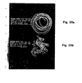
- FIG. 20A is a photograph that shows the undesirable long continuous stringer type of chips. This is in significant contrast to FIG. 20B which shows the tight, short coil type of chip.
- FIG. 21A is a photograph that shows long stringers generated with turning using the coated cutting tool with the as-ground substrate.
- FIG 21B is a photograph that shows the tight, short coil style chips generated while turning using the coated cutting tool having the resintered substrate.
- FIG. 19 is a photograph that shows the long continuous stringer chips formed when turning using an uncoated K11 substrate cutting tool. It is very apparent that a cutting tool with a resintered substrate, wherein the rake face has the requisite surface roughness, provides for much improved chip formation properties over a cutting tool with an as-ground substrate in the turning of 383.2 aluminum alloy.
- a cutting tool with the requisite rake surface roughness has particularly good application for chip control when used to machine so-called "gummy" workpiece materials.
- workpiece materials include aluminum-based alloys, magnesium-based alloys, copper-based alloys, brass alloys, and mild steel alloys such as, for example, AISI 1008 and AISI 1045 steels.
- FIG. 18 shows a view of the cutting tool A-CN82 (resintered with 3.5 ⁇ m TiAlN) so as to illustrate the four corners of the cutting tool including corners 2 and 4.
- the flank face of the cutting tool was buffed at corner 4 after coating.
- the remainder of the cutting tool was not buffed.
- the cutting tool that had the resintered substrate with the thin PVD TiAlN coating formed short coil style chips in contrast to a cutting tool with an as-ground substrate and the thin PVD TiAlN coating.
- the roughness of the coating surface is greatest for those surfaces of the resintered substrate wherein the coating was not buffed.
- the rake and flank surfaces of the as-ground coated cutting tool had surface roughnesses of 9 and 11 microinches R a , (142 and 165 Microinches R tm ) respectively. This is in comparison to the surface roughness of the coating of a resintered substrate not subjected to buffing which were between 54 and 60 microinches R a (348 and 387 microinches R tm ).
- the flank face also resulted in a smoother workpiece surface finish.
- the workpiece surface finish from the as-ground cutting tool was 42 ⁇ 7 microinches R a and the workpiece surface finish from the resintered cutting tool was 48 ⁇ 4 microinches R a . These surfaces finishes are in contrast to 31 ⁇ 2 microinches R a for the cutting tool (CN82/Corner 4) having the buffed flank surface.
- Example EB46-AL comprised the basic as-sintered cemented tungsten carbide substrate with a TiAlN coating applied via PVD for 4 hours to a thickness of about 3.5 micrometers.
- This example presented one embodiment of the invention wherein the thinner single layer coating was applied via PVD to the as-ground substrate.
- Example CN89-RL comprised the basic substrate that was subjected to a resintering prior to the application of the TiAlN coating to a thickness of about 3.5 micrometers in the same coating run as for Example EB46.
- Example CN89-RL is an embodiment of the invention wherein the substrate is resintered prior to the application by PVD of the thinner single layer coating.
- Example CN89-RLB comprised the basic substrate that was subjected to resintering prior to the application of the TiAlN coating to a thickness of about 3.5 micrometers in the same coating run as for Example EB46.
- Example CN89-RLB was then subjected to buffing of the flank face.
- Example CN89-RLB was an embodiment of the invention wherein the substrate was resintered, coated with a single PVD layer, and the flank face of the coated cutting tool buffed.
- Example EB56-AH comprised the basic as-sintered cemented tungsten carbide substrate with a TiAlN coating applied via PVD for 10 hours to a thickness of about 10.5 micrometers.
- This example presented one embodiment of the invention wherein a thicker single layer coating was applied via PVD.
- Example CO08-RH comprised the basic substrate that was subjected to a resintering prior to the application of the TiAlN coating to a thickness of about 10.5 micrometers in the same coating run as for Example EB56-AH.
- Example CO08-RH was an embodiment of the invention wherein the substrate is subjected to resintering prior to the PVD application of the thicker TiAlN coating.
- Example CO08-RHB comprised the basic substrate that was subjected to a resintering prior to the application of the TiAlN coating to a thickness of about 10.5 micrometers in the same coating run as for Example EB56-AH. The flank face of the coated tool was then subjected to buffing.
- Example CO08-RHB was an embodiment of the invention wherein the substrate was subjected to resintering prior to the application of the TiAlN coating, and then the flank face of the coated tool was buffed.
- Example EB66-A comprised the basic as-sintered cemented tungsten carbide substrate with a multi-layer coating applied via a combination of CVD and PVD.
- the coating scheme comprised: the application by CVD of a base layer of TiN that was about 1.0 micrometers thick; the application by CVD of an intermediate layer of TiCN that was about 4.0 micrometers thick, and the application by PVD of a top layer of TiN that was about 4.0 micrometers thick.
- This example presents one embodiment of the invention wherein a multi-layer coating is applied via CVD and PVD to an as-ground substrate.
- Example CQ87-R comprised the basic substrate that was subjected to a resintering prior to the application of the multi-layer coating by CVD and PVD in the same coating run as for Example EB66-A.
- Example CQ87-R is an embodiment of the invention wherein the substrate is subjected to resintering prior to the application of the multi-layer coating.
- Example CQ87-RB comprised the basic substrate that was subjected to a resintering prior to the application of the multi-layer coating by CVD and PVD in the same coating run as for Example EB66-A. The flank face of the coated tool was then subjected to buffing.
- Example CQ87-RB was an embodiment of the invention wherein the substrate was subjected to resintering prior to the application of the multi-layer coating, and then the flank face of the coated tool was buffed.
- the designations for the "Condition” of the tool have the following meanings.
- the designation "A” means that the cutting tool had an as-ground substrate prior to the coating process.
- the designation “R” means that the cutting tool had an as-ground substrate that was resintered prior to the coating process.
- the designation "R & B” means that the cutting tool had an as-ground substrate that was resintered prior to the coating process and the coated flank face of the cutting tool was buffed.
- Tool Life & Failure Mode the tool life is measured in minutes. If the cutting tool remained useful, i.e., did not satisfy a pre-selected failure criterion, after 40 minutes of turning, the test was stopped and the tool life recorded as 40.0+ minutes with no failure occurring. If the cutting tool satisfied one of the pre-selected failure modes, then the tool life at the time of failure was recorded in minutes along with the particular mode of failure. The failure modes are described below.
- the uniform flank wear (“fw”) failure mode occurred when the uniform flank wear reached .015 inches.
- the maximum localized flank wear (“mw”) failure mode occurred when the maximum localized flank wear reached .030 inches.
- the maximum crater depth (“cr”) failure mode occurred when the maximum crater depth as measured from the surface of the rake face reached .004 inches.
- the maximum depth-of-cut notch (“dn”) failure mode occurred when the depth-of-cut notch reached .030 inches.
- the maximum chipping (“ch”) failure mode occurred when the size of the chip reached .030 inches.
- the designation “bk” means that the cutting tool broke.
- this row reflects the condition of the cutting tool at the end of 40 minutes of turning assuming that the cutting tool was turning at the 40 minute point in the test. This row indicates the condition and the extent of wear for that condition in one-thousandths of an inch.
- the corner flaking rating is a numerical rating that rates the extent of corner flaking of the coating.
- the flank flaking rating is a numerical rating that rates the extent of flank flaking of the coating. For both of these ratings, the rating of "5" means that there was no flaking of the coating. The rating of "3” means that there was noticeable flaking. The rating “1” means that there was severe flaking of the coating.
- the rating "4" is between ratings “5" and “3"
- the rating "2" is between ratings "3" and "1".
- the chip flow rating is a numerical rating that rates the extent of chip flow damage to the coating.
- the rating “5" means that there was no damage due to chip flow.
- the rating “3” means that there was noticeable damage due to chip flow.
- the rating “1” means that there was severe chip flow damage.
- the rating "4" is between ratings “5,” and “3”.
- the rating “2” is between ratings “3” and “1”.
- the conventional KC730 cutting tool had a tool life of 2.0 minutes and the failure mode was chipping.
- the corner flaking rating was 2, the flank flaking rating was 5, and the chip flow damage rating was 4.
- the conventional uncoated K11 cutting tool had a tool life of 0.4 minutes and the failure mode was breakage.
- the chip flow damage rating was 4.
- the cutting tools having the as-ground substrate with a single thin (3.5 micrometers) PVD layer of TiAlN experienced much greater tool life in the turning of 304 stainless steel than the conventional cutting tool and the cutting tools having the resintered substrate.
- the as-ground cutting tool (EB46-AL) had a tool life of 40+ minutes as compared to 10 minutes and 2 minutes.
- the cutting tools that had the resintered substrate had the best ratings for corner flaking, flank flaking, and chip flow damage as compared to the cutting tools with the as-ground substrate.
- the average workpiece surface finish was higher, i.e., rougher, for the cutting tool with a resintered substrate. Buffing the flank of the cutting tool with the resintered substrate helped reduce the roughness of the workpiece surface finish.
- the cutting tools having the as-ground substrate with the single thick (10.5 micrometer) PVD layer of TiAlN experienced much greater tool life in the turning of 304 stainless steel than the conventional cutting tool.
- the cutting tools with the resintered substrate and the single thick PVD layer of TiAlN experienced greater tool life than the conventional cutting tool, but less tool life than the as-ground cutting tools.
- the resintered cutting tools had a better corner flaking rating and flank flaking rating than the as-ground cutting tools.
- the as-ground cutting tools had the best chip flow damage rating.
- the as-ground cutting tool resulted in workpiece surface finishes that were the smoothest.
- the resintered cutting tools had the roughest workpiece surface finishes. Buffing reduced the workpiece surface roughness (CO08-RHB).
- the cutting tools with the multi-layer coating experienced improved tool life over that of the conventional cutting tool.
- the resintered cutting tools had excellent corner flaking and flank flaking ratings.
- the as-ground cutting tool had the best chip flow damage rating while the other cutting tools had lower ratings.
- the resintered cutting tools subjected to buffing produced workpieces with the smoothest surface finishes.
- the resintered cutting tools produced workpieces with the roughest surface finishes.
- Example EB46-AL (as-ground low cobalt substrate/ 3.5 ⁇ m TiAlN PVD coating) had a tool life of 40.0+ minutes with no failure.
- Example EB56-AH (as-ground low cobalt substrate/ 10.5 ⁇ m TiAlN PVD coating) had a tool life of 40.0+ minutes with no tool failure.
- Example EB66-A (as-ground low cobalt substrate/CVD-PVD coating) had a tool life of 40.0+ minutes with no failure.
- Example CQ87-R (resintered low cobalt substrate/CVD-PVD coating) had a tool life of 40.0 minutes with failure by chipping.
- Example CQ87-RB (resintered and buffed low cobalt substrate/ CVD-PVD coating) had a tool life of 40.0+ minutes with no failure.
- the use of a low cobalt-WC substrate with any one of the coating schemes results in a tool life that surpasses the comparable conventional cutting tools (KC730 and uncoated Kll).
- coating schemes as set forth in the specification herein have application for use with substrates that present a binder-enriched peripheral layer. When used with the binder-enriched substrates, these coating schemes should have the same advantages and beneficial results that exist with respect to the low cobalt substrates as set forth in this specification.
Abstract
Description
- The present invention relates to a coated cutting tool according to the preamble of
claim 1 and as known for example from US-A-5 075.181. - In particular the invention pertains to a cutting tool, that provides for improved chip control, improved surface finishing properties, and/or improved coating adhesion. The invention further pertains to a coated cutting tool with a low cobalt substrate and having a long tool life.
- More specifically with respect to the chip control properties, the invention pertains to a cutting tool, and a method of making the same, with a rake face having microtopographical properties that provide chip control features without the need for a structural chip breaker. More specifically, the rake surface of the cutting tool has an appropriate surface roughness so as to provide chip control properties.
- In regard to the improved surface finishing properties, the invention concerns a cutting tool, and a method of making the same, that has the capability to machine the workpiece so as to present a smooth machined surface. More particularly, the invention concerns a cutting tool with a flank face that is smooth so as to produce a desirably smooth surface finish on the surface of the workpiece.
- In addition, the invention pertains to a cutting tool, and a method of making the same, having a coating scheme thereon, such as, for example, a single layer coating deposited by physical vapor deposition (PVD) or a multi-layer coating wherein at least one layer is deposited by PVD, wherein the coating has improved adhesion.
- Certain machining operations such as, for example, threading, grooving or cutoff, have the tendency to produce long chip strings or "birds nests". The production of these long chip strings, as opposed to shorter C-shaped/figure six-shaped chips or short coils, are not desirable.
- Certain materials are difficult to machine without creating long chip strings. In other words, due to the very nature of the material there is the tendency to produce long chip strings through any machining operation on these materials. These materials include titanium alloys, aluminum alloys and low carbon steels.
- Earlier cutting tools provide special chip breaker structures or geometries on the rake surface of the cutting tool to break the chips. For example, U.S. Patent No. 4,710,069 to Loquist illustrates a cutting tool that provides a structural chip breaker in the form of a number of depressions that cooperate with the chip breaking face.
- While the structural chip breakers may perform in a satisfactory fashion, the typical geometry of cutting tools with structural chip breakers may be complex. In regard to the manufacture of such cutting tools, a complex geometry requires rams of a complex and intricate design. It can be expensive to make rams that have such a complex and intricate geometry.
- The use of cutting tools with structural chip breakers typically requires there to be an inventory of a number of different styles of cutting tools, each with a different structural chip breaker depending upon the specific application. It can be expensive for the user to inventory many different styles of cutting tools. It can be expensive for the manufacturer of the tools to keep an inventory of many different styles of rams required to make these structural chip breaker geometries.
- Many machining applications require the surface of the machined workpiece to have a certain finish or smoothness. To meet this objective, earlier cutting tools, where necessary, have been ground or polished to present a relatively smooth surface on both the rake face and the flank face. While this arrangement produces a workpiece with a satisfactory surface finish, there is no effective chip control unless such a cutting tool includes a structural chip breaker. The lack of effective chip control in the typical cutting tool having a smooth rake face and a smooth flank face can result in the production of the long chip strings. This is especially true when machining a workpiece material that typically generates long chip strings.
- In the past, coatings like TiAlN have been applied to substrates for cutting tools such as, for example, cemented carbides and cermets, via physical vapor deposition (PVD) techniques such as, for example, sputtering, ion plating and cathodic arc. These substrates have presented a surface that has been relatively smooth in that it has been in an as-ground condition, an as-molded condition, or a grit-blasted condition. Heretofore, the adherence of the PVD coating decreased as the thickness of the coating increased. PVD coating thicknesses had to be held below about 6 micrometers to maintain adequate adherence to the substrate. In the case of the TiAlN PVD coating, the thickness could not exceed about 5 micrometers and still maintain adequate adherence to the substrate for cutting tool applications. Because of the high residual stresses associated with the application of a PVD-applied TiC or cubic Boron Nitride coating, such a coating has not been able to applied at any functional thickness, i.e., a thickness that is sufficient for the cutting tool to be commercially practical, with adequate adhesion strength.
- In the past, persons have used multi-layer coating schemes applied by a combination of chemical vapor deposition (CVD) and PVD techniques. One such example of a multi-layer coating scheme comprises a base layer of TiN applied by CVD, an intermediate layer of TiCN applied by CVD, and a top layer of TiN applied by PVD techniques to a substrate that has binder enrichment in a surface layer. This combination coating scheme is a subject of U.S. Patent No. 5,250,367 to Santhanam et al. entitled BINDER ENRICHED CVD AND PVD COATED CUTTING TOOL, and assigned to the assignee of the present patent application. In U.S. Patent No. 5,250,367 the substrate has a bulk cobalt content of 3 to 12 weight percent with 5 to 8 weight percent and 5.5 to 7 weight percent as more preferable ranges for the cobalt content. Specific examples include cobalt contents of 10.5, 8.5 and 9.5 weight percent cobalt. U.S Patent No. 5,325,747 to Santhanam et al. for METHOD OF MACHINING USING COATED CUTTING TOOLS, and assigned to the assignee of the present patent application, discloses a cutting tool with a substrate that has one or more layers applied by CVD and an outer layer of TiN applied by PVD. In the case where the substrate is a WC-Co material, the cobalt has a range of 3 to 12 weight percent with more preferable ranges of 5 to 7 weight percent and 5.7 to 6.3 weight percent. The specific examples show cobalt contents of 6.0, 8.5, 9.75, 10, 10.5 and 11.5 weight percent. U.S. Patent No. 5,364,209 to Santhanam et al. for CVD AND PVD COATED CUTTING TOOLS, and assigned to the assignee of the present patent application, discloses a cutting tool having a substrate with at least one inner CVD-applied layer and an outer layer applied by PVD. In the case where the substrate is WC-Co, the binder (cobalt) ranges between 5 and 15 weight cobalt with more preferable ranges being between 7 and 13 weight percent and 8 and 12 weight percent cobalt. U.S. Patent No. 5,066,553 to Yoshimura entitled SURFACE-COATED TOOL MEMBER OF TUNGSTEN CARBIDE BASED CEMENTED CARBIDE mentions the resintering of a substrate to achieve better adherence for a CVD applied coating.
- It becomes apparent that the earlier cutting tools have drawbacks. These drawbacks pertain to the chip control properties of the cutting tools, the surface finishing properties of the cutting tools, and the adhesion of the coating to the cutting tool substrate.
- It would be desirable to provide an improved cutting tool, that provides chip control through the microtopography of the rake face of the cutting tool either with or without the use of a structural chip breaker, but preferably without the use of a structural chip breaker. By providing such a cutting tool, one can reduce the costs of manufacture by lowering the cost of manufacturing the rams that form the powder material into the shape of the cutting tool. Such a cutting tool can also lower the cost of manufacture by decreasing the number of rams that the manufacturer must keep in inventory. Such a cutting tool will also reduce the costs associated with selling and distributing cutting tools due to the reduction in the number of cutting tools that the user must keep in inventory.
- It would also be desirable to provide an improved cutting tool, that provides chip control through the microtopography of the rake face of the cutting tool without the use of a structural chip breaker, as well as provides for a smooth machined surface on the workpiece. Such a cutting tool would provide both chip control and result in a smooth surface finish for the machined workpiece.
- It would be desirable to provide for an improved cutting tool, that has a PVD coating that exhibits improved adherence to the substrate, that has thicker PVD coatings, and that permits the use of new adherent PVD-applied coatings such as, for example, TiC, aluminum oxide, and cubic boron nitride.
- It would also be desirable to provide for an improved cutting tool, that has a low cobalt substrate with a coating thereon and which experiences long tool life.
- The present invention is directed to a coated cutting tool having a substrate presenting a surface wherein the surface includes a rake face and flank face with the rake face and the flank face intersecting to form a cutting edge, and a PVD coating on at least a portion of the surface of the substrate, for example, as disclosed in US-Patent No. 5,075,181, which is considered to be the closest prior art. The coated cutting tool according to the invention is characterized in that the portion of the substrate surface which is coated has a surface roughness between about 15 microinches Ra and about 125 microinches Ra; and the PVD coating has an adherence as measured by the Rockwell A indentation adhesion load test of greater than or equal to 60 kg.
- The following is a brief description of the figures which form a part of this patent application:
- FIG. 1 is a perspective view of a first specific embodiment of a coated cutting tool of the invention;
- FIG. 2 is a cross-sectional view of the cutting tool of FIG. 1 taken along section line 2-2 of FIG. 1;
- FIG. 3 is a top view of a second specific embodiment of a coated cutting tool of the invention;
- FIG. 4 is a side view of the cutting tool of FIG. 3;
- FIG. 5 is a cross-sectional view of the cutting tool of FIG. 3 taken along section line 5-5 of FIG. 3;
- FIG. 6 is a perspective view of a third specific embodiment of an uncoated cutting tool of the invention;
- FIG. 7 is a cross-sectional view of the cutting tool of FIG. 6 taken along section line 7-7 of FIG. 6;
- FIG. 8 is a perspective view of a fourth specific embodiment of a coated cutting tool of the invention wherein the flank surface of the substrate has a rough microtopography and the surface of the coated flank face has a rough microtopography;
- FIG. 9 is a cross-sectional view of the cutting tool of FIG. 8 taken along section line 9-9 of FIG. 8;
- FIG. 10 is a perspective view of a fifth specific embodiment of a coated cutting tool of the invention wherein the flank surface of the substrate has a rough microtopography and the surface of the coated flank face has a smooth microtopography, while the rake face of the substrate and the coated tool have a rough microtopography;
- FIG. 11 is a cross-sectional view of the cutting tool of FIG. 10 taken along section line 11-11 of FIG. 10;
- FIG. 12 is a perspective view of a sixth specific embodiment of a coated cutting tool of the invention wherein the rake surface of the substrate has a rough microtopography, the surface of the coated rake face has a smooth microtopography and the flank faces of the substrate and coated tool have a smooth microtopography;
- FIG. 13 is a cross-sectional view of the cutting tool of FIG. 12 taken along section line 13-13 of FIG. 12;
- FIG. 14 is a perspective view of a seventh specific embodiment of a coated cutting tool of the invention wherein there is a multi-layer coating on the substrate;
- FIG. 15 is a cross-sectional view of the cutting tool of FIG. 14 taken along section line 15-15 of FIG. 14;
- FIG. 16 is a perspective view of an eighth specific embodiment of a coated cutting tool of the invention wherein the flank and rake faces of the substrate have a rough microtopography and the coated flank and rake faces have a smooth microtopography;
- FIG. 17 is a cross-sectional view of the cutting tool of FIG. 16 taken along section line 17-17 of FIG. 16;
- FIG. 18 is a schematic top view of the cutting tool sample CN82 which identifies the four corners of the cutting tool and the locations where surface roughness measurements were taken;
- FIG. 19 is a photograph of the "birds nest" type of a chip that was formed from the turning of a 383.2 aluminum alloy workpiece with an uncoated WC-Co cutting tool (uncoated K11);
- FIG. 20A is a photograph of the "birds nest" type of a chip that was formed from the turning of a 383.2 aluminum alloy workpiece with a WC-Co cutting tool comprising an as-ground substrate coated with a single layer of TiAlN;
- FIG. 20B is a photograph of the short desirable type of a chip that was formed from the turning of a 383.2 aluminum alloy workpiece with a WC-Co cutting tool comprising a resintered substrate coated with a single layer of TiAlN;
- FIG. 21A is a photograph of the birds nest type of a chip that was formed from the turning of a 383.2 aluminum alloy workpiece with a WC-Co cutting tool having an as-ground substrate coated with a multi-layer coating scheme of TiN/TiCN/TiN; and
- FIG. 21B is a photograph of the short desirable type of a chip that was formed from the turning of a 383.2 aluminum alloy workpiece with a WC-Co cutting tool coated with a multi-layer coating scheme of TiN/TiCN/TiN wherein the substrate was resintered prior to the coating process.
-
- FIGS. 1 and 2 illustrate a first specific embodiment of the cutting tool of the invention generally designated as 20. Cutting
tool 20 includes asubstrate 22 which has arake face 24 and aflank face 26. The cutting tool substrate may also be made in any of the standard shapes and sizes such as those identified in the American National Standard for Cutting Tools - Indexable Inserts - Identification System, ANSI B212.4-1986. Inserts may also have various chipbreaker structures (not shown) on their rake face as well to facilitate breakage and removal of chips. - The
substrate 22 can be selected from many possible substrate materials suitable for use as a cutting tool substrate. Basic material categories includes tool steels, cemented carbides, cermets, ceramics, ceramic composites, polycrystalline diamond, and polycrystalline cubic Boron Nitride as candidates for a cutting tool substrate. - In the category of cemented carbides, one substrate is a cobalt cemented tungsten carbide composition. In these compositions, the cobalt ranges between about .2 weight percent to about 20 weight percent with the balance consisting essentially of tungsten carbide, and optionally, carbides and carbonitrides with tungsten, titanium, tantalum, zirconium, hafnium and/or niobium.
- In the category of cermets there are titanium carbonitride-based materials having a cobalt and/or nickel binder metal. These cermets include the following grades of cermets sold by Kennametal Inc. of Latrobe, Pennsylvania (assignee of the present patent application): KT125, KT150, KT175, and KT195.
- In the category of ceramics there are silicon nitride-based, or aluminum oxide-based, ceramics with or without reinforcement additives such as silicon carbide and titanium carbide in whisker or particulate form.
- In the category of ceramic composites there are whisker reinforced ceramics. Examples of these types of composites includes silicon carbide whiskers and/or titanium carbide whiskers in an alumina matrix.
- A
coating 28 covers therake face 24 and theflank face 26 of thesubstrate 22. The use of acoating 28 may or may not be necessary depending upon the specific application and the specific substrate of the cutting tool. In those cases where coatings are used, there are many variations for a coating scheme. - A single or multi-layer coating may be applied by physical vapor deposition techniques. One such example is a coating of TiAIN or TiN applied by PVD. One example of a multi-layer coating is a TiN-TiCN-TiN coating scheme such as that mentioned in U.S. Patent No. 5,250,367 to Santhanam et al. which discloses coating schemes that comprise a combination of CVD and PVD techniques or U.S. Patent 5,075,181 to Quinto et al. which discloses a multi-layer coating scheme applied solely by PVD techniques.
- Alternatively or in addition to TiAlN, coating layers may be used for cutting tools include the carbides, nitrides, carbonitrides and borides of zirconium, titanium, hafnium and their alloys, alumina, cubic Boron Nitride, silicon nitride, and a thin film polycrystalline diamond layer.
- Referring back to the
substrate 22, therake face 24 of thesubstrate 22 consists of a microscopically rough surface. Theperipheral edge 30 of thesubstrate 22 is at the joinder of therake face 24 and theflank face 26. Theflank face 26 presents a relatively smooth surface. - In regard to the
coating 28, coating 28 is illustrated in the first specific embodiment (FIG. 2) as a single layer. Thecoating 28 overlies thesubstrate 22 so that the completecoated cutting tool 20 presents an exposedrake face 34 and an exposedflank face 36. The exposedrake face 34 has a microscopically rough surface. The exposedflank face 36 presents a relatively smooth surface as compared to the rake face. The exposedperipheral edge 38 is at the juncture of therake face 34 andflank face 36. - The roughness of the
rough rake surface 24 for thesubstrate 22, and for the exposedrake face 34 range between 15 microinches Ra and 125 microinches Ra as measured on a Sheffield Proficorder Spectre Unit. A preferable range for this surface roughness is between 25 microinches Ra and 125 microinches Ra. An even more preferable range is between 40 microinches Ra and 80 microinches Ra. - Preferably, the roughness of the exposed
smooth flank face 36 is less than 25 microinches Ra as measured on a Sheffield Proficorder Spectre Unit. A more preferable surface roughness is less than 15 microinches Ra. - The specific embodiment of the cutting tool of FIGS. 1 and 2 presents the advantage of good adhesion of the coating on the rake face of the substrate due to the surface roughness of the rake face of the substrate. This cutting tool has good chip control due to the surface roughness on the coated rake face. This specific embodiment also exhibits good workpiece surface finish characteristics due to the smooth surface of the coated flank face.
- Referring to FIGS. 3 through 5, these drawings illustrate a second specific embodiment of the cutting tool of the invention generally designated as 42. Cutting
tool 42 includes a substrate 44 (see FIG. 5) that presents arake face 46 and a flank face 48. A coating 50 overlies therake face 46 and the flank face 48. The types of substrates and coatings available for cuttingtool 42 are the same as those available for cuttingtool 20. - The
substrate 44 includes aperipheral edge 54 which is at the joinder of therake face 46 and the flank face 48. Thesubstrate 44 has a peripheralrough surface portion 56, i.e., a portion of the surface that is microscopically rough, which extends inwardly from theperipheral edge 54 of thesubstrate 44. Astructural chip breaker 58, which has a microscopically rough surface, extends inwardly from the inward edge of the peripheralrough surface portion 56. - The
substrate 44 further includes a microscopically rough central surface portion 60. Central surface portion 60 is bounded by thestructural chip breaker 58. - The coating 50 (see FIG. 5) overlies the
substrate 44 to form thecoated cutting tool 42 that has an exposedrake face 64 and an exposedflank face 66. The coating 50 has aperipheral edge 70 at the joinder of the exposedrake face 64 and the exposedflank face 66 of thecoated cutting tool 42. - There is an exposed peripheral microscopically rough exposed
rake face portion 72 that extends inwardly from theperipheral edge 70. An exposedstructural chip breaker 74 then extends inwardly from the peripheral microscopically rough exposedrake face portion 72.Structural chip breaker 74 has a microscopically rough surface. The exposedrake face 64 further includes acentral portion 76 that presents a rough surface. The cuttinginsert 42 contains acentral hole 78. - The roughness of the rake surface portions (56, 58, 60) of the substrate and of the exposed rake face portions (72, 74, 76) are the same as described above for
rough rake surface 24. The roughness of the flank 48 surface of thesubstrate 22 and the exposed flank face is the same as described above for thesmooth flank face 36. In another option, thecentral portion 76 of the rake face may have a relatively smooth surface. - The specific embodiment of FIGS. 3 through 5 presents a cutting tool that has good adhesion of the coating to the rake face of the substrate because of the surface roughness of the rake face of the substrate. This cutting tool has good chip control properties due to the surface roughness of the coated rake face of the cutting tool. This cutting tool presents good workpiece surface finishing properties due to the smooth surface of the coated flank face.
- Referring to FIGS. 6 and 7, there is illustrated an uncoated cutting tool generally referred to as 90. The
uncoated cutting tool 90 can be made from any cutting tool material suitable for use in an uncoated condition. - The
uncoated cutting tool 90 includes arake face 92 and aflank face 94. The rake face 92 presents a microscopically rough surface. Theperipheral edge 96 is at the joinder of therake face 92 and theflank face 94. The roughness of therough rake face 92 is the same as that described above forrough rake surface 24. The roughness of theflank surface 94 is the same as that described above for thesmooth flank face 36. - The uncoated cutting tool of FIGS. 6 and 7 exhibits good chip control properties due to the rough surface of the rake face of the cutting tool and provides smooth workpiece finishes due to the smooth flank surfaces of the cutting tool.
- Referring to FIGS. 8 and 9, there is illustrated another specific embodiment of the cutting tool of the invention, generally designated as 100. Cutting
tool 100 has asubstrate 102 with arake face 104 and a flank face 106. Therake face 104 is rough, i.e., has a rough surface microtopography. The flank face 106 of the substrate also has a rough microtopography. Cuttingtool 100 includes acoating 108 that overlies the surfaces of thesubstrate 102. Therake face 110 of the coated cutting tool has a rough microtopography and theflank face 112 of the coated cutting tool also has a rough microtopography. The surface roughness of the coated rake and flank faces (110, 112) is the same as described above for therough rake surface 24. - The specific cutting tool of FIGS. 8 and 9 exhibits good coating adherence to the rake and flank faces due to the rake and flank faces of the substrate having a surface roughness. This cutting tool provides good chip control properties due to the surface roughness of the coated rake face, but somewhat rougher workpiece surface finishes due to the surface roughness of the coated flank faces.
- Referring to FIGS. 10 and 11, there is illustrated another specific embodiment of the cutting tool of the invention, generally designated as 120. Cutting
tool 120 has asubstrate 122 with arake face 124 and aflank face 126. Therake face 124 is rough, i.e., has a rough surface microtopography. Theflank face 126 also has a rough microtopography. Cuttingtool 100 includes acoating 128 that overlies the surfaces of thesubstrate 122. Therake face 130 of the coated cutting tool has a rough microtopography. The surface roughness of the rake and flank faces (124, 126) of thesubstrate 122 and thecoated rake face 130 are the same as that described above for therough rake surface 24. - The
flank face 132 of the coated cutting tool has a smooth microtopography. To achieve the smooth microtopography on the flank face of the coated tool, the flank face had to be subjected to a polishing or other treatment to smooth the surface. This is especially true in light of the fact that the flank face of the substrate has a rough microtopography. The surface roughness of thecoated flank face 132 is the same as described above for thesmooth flank face 36. - The cutting tool of FIGS. 10 and 11 provides the advantage of good coating adherence to the rake and flank faces of the substrate due to the surface roughness of the rake and flank faces of the substrate. This cutting tool also exhibits good chip control due to the surface roughness of the coated rake face. The cutting tool further provides good workpiece surface finish characteristics due to the smoothness of the surface of the coated flank face.
- Referring to FIGS. 12 and 13, there is illustrated another specific embodiment of the cutting tool of the invention, generally designated as 140. Cutting
tool 140 has asubstrate 142 with arake face 144 and aflank face 146. Therake face 144 is rough, i.e., has a rough surface microtopography. Theflank face 126 has a smooth microtopography. Cuttingtool 140 includes acoating 148 that overlies the surfaces of thesubstrate 142. Therake face 150 of the coated cutting tool has a smooth microtopography. Theflank face 152 of the coated cutting tool also has a smooth microtopography. To achieve the smooth microtopography on the rake face of the coated tool, the rake face had to be subjected to a polishing or other treatment to smooth the surface. This is especially true in light of the fact that the rake surface of the substrate has a rough microtopography. - The surface roughness of the
rake face 144 of the substrate is the same as described above forrough rake surface 24. The surface roughness of theflank face 146 of the substrate and the coated rake and flank faces (150, 152) is the same as described above for thesmooth flank face 36. - The cutting tool of FIGS. 12 and 13 provides good adherence of the coating to the rake face of the substrate due to the surface roughness of the rake face of the substrate. This cutting tool provides for good workpiece surface finishing properties due to the smooth surface of the coated flank face. This cutting tool also provides for reduced tendency for a built-up edge on the coated rake face due to the surface smoothness of the rake face of the coated cutting tool.
- Referring to FIGS. 14 and 15, there is illustrated another specific embodiment of the cutting tool of the invention, generally designated as 160. Cutting
tool 160 has asubstrate 162 with arake face 164 and aflank face 166. Therake face 164 is rough, i.e., has a rough surface microtopography. Theflank face 166 has a smooth microtopography. Cuttingtool 160 includes a multi-layered coating that overlies the surfaces of thesubstrate 162. The coating comprises abase layer 168, anintermediate layer 170, and atop layer 172. Therake face 174 of the coated cutting tool has a rough microtopography. Theflank face 172 of the coated cutting tool has a smooth microtopography. - The surface roughness of the
rake face 164 of the substrate and thecoated rake face 174 is the same as described above forrough rake surface 24. The surface roughness of therake face 166 of the substrate and thecoated flank face 176 is the same as described above for thesmooth flank face 36. - The cutting tool of FIGS. 14 and 15 exhibits good coating adherence to the rake surface of the substrate due to the surface roughness of the rake face of the substrate, as well as the surface roughness of the overlying coating layers. This cutting tool exhibits good chip control properties due to the surface roughness of the exposed coated rake face. The cutting tool has good workpiece surface finishing properties due to the surface smoothness of the coated flank face.
- Referring to FIGS. 16 and 17, there is illustrated another specific embodiment of the cutting tool of the invention, generally designated as 180,. Cutting
tool 180 has asubstrate 182 with arake face 184 and aflank face 186. Therake face 184 is rough, i.e., has a rough surface microtopography. Theflank face 186 also has a rough microtopography. The surface roughness of the rake and flank faces (184, 186) of thesubstrate 182 is the same as that described above for therough rake surface 24. - Cutting
tool 180 includes acoating 188 that overlies the surfaces of thesubstrate 182. Therake face 190 of the coated cutting tool has a smooth microtopography. Theflank face 192 of the coated cutting tool also has a smooth microtopography. To achieve the smooth microtopography on the rake and flank faces of the coated tool, these faces had to be subjected to a polishing or other treatment to smooth the surface thereof. This is especially true in light of the fact that the rake surface and flank surface of the substrate has a rough microtopography. The surface roughness of the coated rake and flank faces (190, 192) is the same as described for thesmooth flank face 36. - The cutting tool of FIGS. 16 and 17 has good coating adhesion to the rake and flank surfaces of the substrate due to the rough rake and flank surfaces of the substrate. This cutting tool has a reduced tendency for a built-up edge on the coated rake face due to the surface smoothness of the coated rake face. This cutting tool provides a good workpiece surface finish due to the surface smoothness of the coated flank face of the cutting tool.
- In regard to the manufacture of the cutting tools, the basic substrate is preferably made by conventional powder metallurgical techniques. More specifically, the powder components of the substrate are blended and pressed into a green compact. The green compact is then subsequently heat treated, such as by sintering, so as to form a substantially fully dense substrate (in the case of a coated cutting tool) or the uncoated cutting tool. In the alternative, a powder blend can be formed into a substantially fully dense body by the simultaneous application of heat and pressure such as, for example, by hot pressing. There are, however, several variations on the densification process necessary to form a substrate with the selective rough surfaces.
- One variation of the sintering process of making the substantially fully dense substrate is to use a ram that forms the powder into the green compact which will form the necessary surface roughness in the green compact. By providing a surface roughness in the green compact of an appropriate degree and dimension, there is provided an as-sintered substrate with the appropriate surface roughness at selected positions on the surface of the substrate. The use of a ram with the necessary surface roughness is also available for the hot pressing process.
- If the surface roughness of the as-sintered (or substantially fully dense) tool is excessive, only the undesirably rough locations of the tool may be ground, polished, laser glazed, or otherwise finished to produce the necessary level of smoothness. This necessary level of smoothness may, in the case of the flank face, be sufficient to generate a smooth workpiece finish in cutting, yet still leave the rough rake surface of the tool intact to produce the desired chip-flow control. In the case of the rake face, the level of smoothness may be sufficient to reduce the tendency for a built-up edge on the rake face. The flank surface of the substrate may be in a rough condition so as to improve the coating adhesion on the flank surface of the substrate.
- Depending on the tool material and cutting application, the tool may be used as-is in the above described condition. In other words, the tool may be used in an uncoated condition. More commonly, however, this tool will serve as a substrate for a protective wear-resistant coating applied by CVD or PVD methods and then used in the cutting application.
- The coating process parameters as known to those skilled in the art are such that the roughness characteristic of the rake and flank surfaces of the tool may be unchanged from that of the substrate prior to the coating operation. In general, however, for the typical CVD and PVD coating processes, the surface roughness of the coated tool is a function of the roughness of the underlying substrate surface and the thickness of the deposited coating. Generally speaking, as the coating thickness increases, the surface roughness of the coating also tends to increase regardless of the underlying surface roughness of the substrate. This could result in the exposed coated surfaces somewhat rougher than the surfaces of the substrate, however, such an increase in surface roughness of the rake surface of the substrate is not deleterious to the desirable chip control properties. The increase in surface roughness of the substrate does not negatively impact on the adhesion of the coating to the substrate, but will typically improve the adhesion.
- An increase in surface roughness of the coated flank surface of the tool, however, could adversely affect the workpiece surface finish generated by the tool. For this reason, a post coating operation such as polishing, buffing, or laser glazing all of some of the flank surfaces of the tool may be required to smooth the surface of the coating to an acceptable surface smoothness, thus, providing acceptably smooth workpiece finishes in the cutting operation.
- An increase in the surface roughness of the coated rake surface may generate a problem of a built up edge, i.e., material from the chip is welded to the rake surface of the cutting tool. To reduce the potential for a problem of a built up edge, a post coating operation such as polishing, buffing, or laser glazing all or some of the rake surfaces of the tool may be required to smooth the surface of the coating to an acceptable surface smoothness, thus, reducing the potential for the occurrence of a built up edge. The built-up edge is a problem that is workpiece material dependent. While smoothing the rake surface reduces chip control properties, it still leaves the coating with good adhesion due to the surface roughness of the rake face of the substrate.
- Still another variation on the basic process uses an additional resintering step after the initial processing of the substrate. The purpose of the resintering is to enlarge the grains of the substrate, e.g., tungsten carbide, at the surface so as to form a rough irregular surface. The irregular surface presents a surface with the necessary roughness. This process is a subject of a pending United States patent application Serial No. 08/159,272 filed on November 30, 1993 entitled DIAMOND COATED TOOLS AND PROCESS FOR MAKING which is assigned to the assignee of the applicant herein. The above United States patent application Serial No. 08/159,272 filed on November 30, 1993 entitled DIAMOND COATED TOOLS AND PROCESS FOR MAKING is hereby incorporated by reference herein.
- In this variation that uses resintering in conjunction with the cemented tungsten carbide substrate, the surface of an as-sintered tungsten carbide based cemented carbide substrate is composed of tungsten carbide hard grains bound together by cobalt or a cobalt alloy. The cobalt is not only between the tungsten carbide grains, but also covers some of the tungsten carbide grains at the substrate surface due to the wetting properties of Co and tungsten carbide under vacuum sintering conditions.
- Now in accordance with the present invention, the as-sintered and ground substrate described above is now resintered under time, temperature and atmospheric conditions, to cause grain growth and binder depletion from its surfaces. The time and temperature are selected such that sufficient grain growth occurs on the surface of the resintered substrate to produce a surface roughness, Ra, in the ranges set out above for the
rough rake surface 24. - The resintering times required to achieve the required surface roughness will depend on the starting material and the sintering conditions. As temperature increases, resintering times should decrease. For some cemented tungsten carbide compositions, resintering times of 2 to 3 hours at 1510°C (2750°F) have been found to be sufficient to provide the needed surface roughness. If the desired surface roughness is not produced after the first resintering treatment, the substrate may be resintered again until the desired surface roughness is produced.
- It is believed that the atmosphere during the resintering treatment may also be important to obtaining good coating adhesion to the substrate. It is believed that if a nitrogen atmosphere is utilized during this treatment, the amount of cobalt on the resulting rough surface will be minimized. The nitrogen partial pressure should be controlled to allow cobalt evaporation from the surface. During the resintering one should minimize re-wetting of the surface by additional cobalt from the bulk of the substrate.
- The most beneficial nitrogen partial pressure may, therefore, be a function of the substrate composition. Nitrogen partial pressure may also be controlled or varied during the resintering cycle(s) to control the amount and rate of cobalt evaporation from the bulk of the substrate. It is believed that a 0.3 to 50 torr, preferably, 0.3 to 5, and more preferably, 0.3 to 2 torr nitrogen atmosphere should be utilized. It is theorized that the nitrogen atmosphere may allow cobalt on the exterior surfaces of the grains on the substrate surface to evaporate, while sufficient cobalt remains between the surface tungsten carbide grains to keep them well bonded to the remainder of the substrate. Cobalt surface evaporation is accompanied by tungsten carbide grain growth at the surface, resulting in surface roughening.
- After the completion of the resintering process, the substrate may then be coated by physical vapor deposition techniques, chemical vapor deposition techniques, or a combination of techniques that includes physical vapor deposition techniques. The tool in this condition may be CVD or PVD coated prior to use. If the as-resintered tool is coated directly, the outermost surface of the coating on flank surfaces will preferably be smoothed by polishing, buffing, laser glazing, or the like in the zone that comes in contact with the workpiece in order that the tool generates the smoothest workpiece surface finish in the cutting operation.
- In regard to the surface roughness of the coated cutting tool, the roughness of the rake surface has the same ranges as set out above for the
rough rake surface 24. As described above, peripheral grinding, polishing, buffing, or laser glazing the flank surface of the tool will smooth the flank surface while leaving the rough rake surface intact. Typically, the flank face is subjected to buffing so that the roughness of the flank surface is in the same ranges set out above for thesmooth flank face 36. - Still another variation on the process of making the basic substrate is to grind, EDM (electric discharge machine), or laser etch a surface roughness into the as-sintered substrate at selected positions on the surface of the rake face. For all of the variations set forth above, if the surface of the flank face of the as-sintered substrate is sufficiently smooth then no further processing is necessary. Typically, if the cutting tool is coated, it is the coating on the flank surface that will be polished, buffed, or laser glazed to achieve the necessary smoothness.
- While cutting tools, especially those made from cemented tungsten carbide, are typically fabricated by cold pressing and vacuum (i.e., at a pressure of about 10-2 to 10-3 torr) sintering techniques, it should be understood that any of conventional techniques may be used to obtain the basic as-sintered substrate for the present invention. Examples
- In order to demonstrate the advantages and benefits provided by the present invention, a number of examples, and the results of testing of such examples, are set forth hereinafter.
- For all of the examples which are set forth below, unless designated otherwise, the starting substrate was a cobalt cemented tungsten carbide of the following composition and properties: 2.3 to 2.9 weight percent Co; up to 0.4 weight percent Ta; up to 0.1 weight percent Ti; up to 0.1 weight percent Nb and other impurities; and the balance being WC. Other properties of the as-sintered substrate were a Rockwell A hardness between 92.8 and 93.6, a coercive force, Hc, between 290 and 440 oersteds, a magnetic saturation sufficient to avoid the formation of eta phase, the average WC grain size was between 1-6 micrometers, the porosity rating was A08, BOO, COO or better, and the density was between 15.10 to 15.50 grams/cc.
- For all of the examples, the cutting tool that was used was a SPG-422 (.0005 inch radius hone) style of tool, which did not have a structural chip breaker.
- For those examples that were subjected to resintering, the resintering was performed at 2750°F for three hours in about 0.5 torr nitrogen atmosphere to produce a surface roughness of above 45 microinches Ra. Resintering of the as-sintered and ground substrate typically results in the reduction of the cobalt content in the resintered substrate due to cobalt evaporation at the surface during the resintering process.
- For those examples that were subjected to buffing, the buffing was performed for two minutes per edge using a nylon brush whose bristles were impregnating with 120 mesh diamond grit rotating at a speed of 1000 rpm. The brush is available from Jason, Inc. of Cleveland, Ohio.
- To evaluate the adherence of various coatings to the substrate of the cutting tool, the following examples; namely, Examples EB46, CN88, CN89, EB56, CO07, CO08, EB66, CQ87, and CQ88, were tested for coating adherence using an indentation adhesion load test. In this regard, adhesion between the coating and the substrate was determined by an indentation adhesion test using a Rockwell hardness tester with a Rockwell A scale Brale cone shaped diamond indenter at a selected load range of 15kg, 30kg, 45kg, 60kg and 100kg. The adhesive strength was defined as the minimum load at which the coating debonded and/or flaked. Measurements were performed at two sites on the inserts. The measurements of "100 +" indicate that the coating did not debond or flake at the load of 100kg, which was the maximum load used in these tests.
- A description of these examples is set forth below.
- Example EB46 comprised the basic as-sintered cemented tungsten carbide substrate with a TiAlN coating applied via PVD for 4 hours in a CC800 reactor from CemeCon GmbH of Aachen, Germany. This reactor used a magnetron sputtering process to apply the TiAlN. The TiAlN coating had a thickness of about 3.5 micrometers. This example presented one embodiment of the invention wherein a thin single layer coating was applied via PVD to the as-ground substrate.
- Example CN88 comprised the basic as-sintered and ground substrate that was subjected to a resintering as described above prior to the application of the TiAlN coating to a thickness of about 3.5 micrometers in the same coating run as for Example EB46. Example CN88 was an embodiment of the invention wherein the substrate was subjected to resintering prior to the application of the thinner TiAlN coating.
- Example CN89 was the same as Example CN88.
- Example EB56 comprised the basic as-sintered and ground cemented tungsten carbide substrate with a TiAlN coating applied via PVD for 10 hours in the CC800 reactor from CemeCon GmbH of Aachen, Germany. The TiAlN coating had a thickness of about 10.5 micrometers. This example was an embodiment of the invention wherein a thicker single layer coating was applied via PVD to an as-ground substrate.
- Example CO07 comprised the basic substrate that was subjected to a resintering (as described above) prior to the application of the TiAlN coating to a thickness of about 10.5 micrometers in the same coating run as for Example EB56. Example CO07 was an embodiment of the invention wherein the substrate was subjected to resintering prior to the application of the thicker TiAlN coating.
- Example CO08 was the same as Example CO07.
- Example EB66 comprised the basic as-sintered and ground cemented tungsten carbide substrate with a multi-layer coating applied via a combination of CVD and PVD. The coating scheme comprised: the application by CVD of a base layer of TiN that was about 1.0 micrometers thick; the application by CVD of an intermediate layer of TiCN that was about 4.0 micrometers thick, and the application by PVD of a top layer of TiN that was about 4.0 micrometers thick. This example presented one embodiment of the invention wherein a multi-layer coating was applied via CVD and PVD to an as-ground substrate.
- Example CQ87 comprised the basic substrate that was subjected to a resintering (as described above) prior to the application of the multi-layer coating in the same coating run as for Example EB66. Example CQ87 was an embodiment of the invention wherein the substrate was subjected to resintering prior to the application of the multi-layer coating.
- Example CQ88 was the same as Example CQ87.
- The results of the indentation load testing in kilograms is set forth below in Tables I through III. Two measurements were taken for each cutting tool. A higher indentation load test result equates to better coating adherence.
Indentation Load Test Results for Substrate with a 3.5 µm TiAlN PVD Coating Example Condition of the Substrate Indentation Load (kg) at Failure EB46 as-ground 45, 60 CN88 resintered 100+, 100+ CN89 resintered 100+, 100+ Indentation Load Test Results for Substrate with a 10.5 µm TiAlN PVD Coating Example Condition of the Substrate Indentation Load (kg) at Failure EB56 as- ground 30, 30 CO07 resintered 60, 60 CO08 resintered 100+, 100+ Indentation Load Test Results for Substrate with a CVD-PVD Coating Example Condition of the Substrate Indentation Load (kg) at Failure EB66 as-ground 60, 60 CQ87 resintered 45, 60 CQ88 resintered 45, 45 - Three samples of a conventional prior art cutting tool (KC730) coated with TiN to a thickness of about 3.5 micrometers by ion plating on a cemented carbide substrate containing about 6 weight percent cobalt were tested for the indentation adhesion load, and the results of two measurements per cutting tool were 30kg, 45kg for each one of the three cutting tools.
- Referring to Table I, the indentation load results show that for cutting tools having a thinner (about 3.5 micrometer) PVD coating of TiAlN, the adherence of the coating showed significant improvement for those cutting tools having substrates that were resintered after initial sintering and prior to coating. In this regard, Sample Nos. CN88 and CN89 each showed indentation load results of 100+Kg as compared to sample EB46 which had indentation adhesion load measurements of 45kg and 60kg. A comparison of the results of Table I against those for the KC730 cutting tool show that the adhesion of the thinner TiAlN coating (samples CN88 and CN89) improves more than two to three times over that of a comparable conventional cutting tool (KC730) when the substantially fully dense substrate is resintered prior to coating.
- Referring to Table II, the indentation load results show that the adherence of a thicker (about 10.5 micrometers) coating of TiAlN applied via PVD techniques to an as-ground tool is about the same as that of a conventional cutting tool (KC730) as measured in accordance with the indentation load test. The adherence of the thicker PVD coating is significantly improved over that of the conventional KC730 cutting tool when the substantially fully dense substrate has been resintered before coating.
- Referring to Table III, the indentation load results show that for the multi-layer coating [CVD-TiN/CVD-TiCN/PVD-TiN] there is no significant difference in the indentation adherence load test results between the cutting tools with an as-ground substrate and the cutting tools with a resintered substrate.
- Overall, it is apparent that for the cutting tools having the single layer of TiAlN, whether it is about 3.5 micrometers thick or about 10.5 micrometers thick, the resintering of the as-ground substrate significantly improves the coating adhesion strength. The resintering of the as-ground substrate for cutting tools with a CVD-PVD coating does not appear to significantly improve the adherence of the coating to the substrate.
- Samples of certain ones of the above cutting tools, as well as two conventional cutting tools, were used to turn 383.2 aluminum (11 weight percent silicon) alloy under the following conditions: speed of 2500 sfm, feed of .005 inches per revolution, depth of cut of .025 inches, and flood coolant. The results of the these turning test are set forth below in Table IV.
Chip Formation Test Results Example Condition of the Substrate Chip Character (FIG. that shows the chips) Uncoated Substrate as-ground, no coating long continuous stringers, "birds nest" (FIG. 19) KC730 Cutting Tool as-ground long continuous stringers, "birds nest" Cutting Tool like EB46 ( 3.5 µm TiAlN coating) as-ground long continuous stringers, "birds nest" (FIG. 20A) Cutting Tool like CN88 ( 3.5 µm TiAlN coating) resintered short coils (FIG.20B) Cutting Tool like EB66 (CVD-PVD coating scheme) as-ground long continuous stringers, "birds nest" (FIG. 21A) Cutting Tool like CQ87 (CVD-PVD coating scheme) resintered short coils (FIG.21B) - Referring to Table IV, the test results for turning 383.2 aluminum alloy reveal that the use of the substrate that had been resintered provides for much improved chip formation properties. The cutting tools that used resintered substrates, whether in conjunction with a single thin layer (about 3.5 micrometers) of TiAlN or in conjunction with a multi-layer coating scheme, formed chips in the form of short coils. The short coil style of chip is a desirable chip style.
- This is shown in a dramatic fashion for the single thin layer of TiAlN by a comparison of FIG. 20A with FIG. 20B. FIG.. 20A is a photograph that shows the undesirable long continuous stringer type of chips. This is in significant contrast to FIG. 20B which shows the tight, short coil type of chip.
- A comparison of FIG. 21A and 21B also shows the significant difference in chip formation between the CVD-PVD coated cutting tools having the as-ground substrate or the resintered substrate. FIG. 21A is a photograph that shows long stringers generated with turning using the coated cutting tool with the as-ground substrate. FIG 21B is a photograph that shows the tight, short coil style chips generated while turning using the coated cutting tool having the resintered substrate.
- The formation of short coils for those cutting tools having a resintered substrate was also in contrast to the chip formation of the conventional uncoated K11 substrate cutting tool and the conventional coated KC730 cutting tool. FIG. 19 is a photograph that shows the long continuous stringer chips formed when turning using an uncoated K11 substrate cutting tool. It is very apparent that a cutting tool with a resintered substrate, wherein the rake face has the requisite surface roughness, provides for much improved chip formation properties over a cutting tool with an as-ground substrate in the turning of 383.2 aluminum alloy.
- Applicant believes that a cutting tool with the requisite rake surface roughness has particularly good application for chip control when used to machine so-called "gummy" workpiece materials. These workpiece materials include aluminum-based alloys, magnesium-based alloys, copper-based alloys, brass alloys, and mild steel alloys such as, for example, AISI 1008 and AISI 1045 steels.
- Turning tests on 383.2 aluminum alloy under the conditions set forth above was also performed using Examples EB46 and CN82. The results of these tests are set forth in Table V below. FIG. 18 shows a view of the cutting tool A-CN82 (resintered with 3.5 µm TiAlN) so as to illustrate the four corners of the cutting
tool including corners corner 4 after coating. The remainder of the cutting tool was not buffed.Surface Roughness Characteristics of Cutting Tools and the Workpiece Surface Finish Tool Material Surface Condition Prior to Coating Tool Surface Buffed After Coating A-EB46 As-ground Rake
FlankNo
NoA-CN82 (Corner 2) Resintered Rake
FlankNo
NoA-CN82 (Corner 4) Resintered Rake
FlankNo
YesTool Material Coating Surface Roughness (µinches Ra) Coating Surface Roughness (µinches Rtm) Workpiece Surface Finish (µinches Ra) Chip Character A-EB46 9 (r)
11(f)142 (r)
165 (f)42±7 Long continuous stringers A-CN82 (Corner 2) 55 (r)
80 (f)354 (r)
387 (f)48±4 Short Coils A-CN82 (Corner 4) 54 (r)
8 (f)348 (r)
55 (f)31±2 Short Coils - In the coating surface roughnesses reported in Table V above, the use of the "(r)" means the roughness on the rake face of the cutting tool, and the "(f)" means the roughness on the flank face of the cutting tool.
- Referring to Table V, the cutting tool that had the resintered substrate with the thin PVD TiAlN coating (CN82) formed short coil style chips in contrast to a cutting tool with an as-ground substrate and the thin PVD TiAlN coating. The roughness of the coating surface is greatest for those surfaces of the resintered substrate wherein the coating was not buffed. For example, the rake and flank surfaces of the as-ground coated cutting tool had surface roughnesses of 9 and 11 microinches Ra, (142 and 165 Microinches Rtm) respectively. This is in comparison to the surface roughness of the coating of a resintered substrate not subjected to buffing which were between 54 and 60 microinches Ra (348 and 387 microinches Rtm).
- Buffing the flank face of the cutting tool with the resintered substrate did much to smooth the surface and therefore decrease the surface roughness. A comparison between opposite corners of sample CN82 shows that buffing decreased the surface roughness of the coating from 60 to 8 microinches Ra (387 to 55 microinches Rtm)
- Buffing the flank face also resulted in a smoother workpiece surface finish. In this regard, the workpiece surface finish from the as-ground cutting tool was 42±7 microinches Ra and the workpiece surface finish from the resintered cutting tool was 48±4 microinches Ra. These surfaces finishes are in contrast to 31±2 microinches Ra for the cutting tool (CN82/Corner 4) having the buffed flank surface.
- The examples described below; namely, Examples EB46-AL, CN89-RL, CN89-RLB, EB56-AH, CO08-RH, CO08-RHB, EB66-A, CQ87-R and CQ87-RB, were used to turn 304 stainless steel under the following conditions: speed of 800 sfm, feed of .008 inches per revolution, depth of cut of .060 inches, flood coolant, and a 15° lead angle.
- Example EB46-AL comprised the basic as-sintered cemented tungsten carbide substrate with a TiAlN coating applied via PVD for 4 hours to a thickness of about 3.5 micrometers. This example presented one embodiment of the invention wherein the thinner single layer coating was applied via PVD to the as-ground substrate.
- Example CN89-RL comprised the basic substrate that was subjected to a resintering prior to the application of the TiAlN coating to a thickness of about 3.5 micrometers in the same coating run as for Example EB46. Example CN89-RL is an embodiment of the invention wherein the substrate is resintered prior to the application by PVD of the thinner single layer coating.
- Example CN89-RLB comprised the basic substrate that was subjected to resintering prior to the application of the TiAlN coating to a thickness of about 3.5 micrometers in the same coating run as for Example EB46. Example CN89-RLB was then subjected to buffing of the flank face. Example CN89-RLB was an embodiment of the invention wherein the substrate was resintered, coated with a single PVD layer, and the flank face of the coated cutting tool buffed.
- Example EB56-AH comprised the basic as-sintered cemented tungsten carbide substrate with a TiAlN coating applied via PVD for 10 hours to a thickness of about 10.5 micrometers. This example presented one embodiment of the invention wherein a thicker single layer coating was applied via PVD.
- Example CO08-RH comprised the basic substrate that was subjected to a resintering prior to the application of the TiAlN coating to a thickness of about 10.5 micrometers in the same coating run as for Example EB56-AH. Example CO08-RH was an embodiment of the invention wherein the substrate is subjected to resintering prior to the PVD application of the thicker TiAlN coating.
- Example CO08-RHB comprised the basic substrate that was subjected to a resintering prior to the application of the TiAlN coating to a thickness of about 10.5 micrometers in the same coating run as for Example EB56-AH. The flank face of the coated tool was then subjected to buffing. Example CO08-RHB was an embodiment of the invention wherein the substrate was subjected to resintering prior to the application of the TiAlN coating, and then the flank face of the coated tool was buffed.
- Example EB66-A comprised the basic as-sintered cemented tungsten carbide substrate with a multi-layer coating applied via a combination of CVD and PVD. The coating scheme comprised: the application by CVD of a base layer of TiN that was about 1.0 micrometers thick; the application by CVD of an intermediate layer of TiCN that was about 4.0 micrometers thick, and the application by PVD of a top layer of TiN that was about 4.0 micrometers thick. This example presents one embodiment of the invention wherein a multi-layer coating is applied via CVD and PVD to an as-ground substrate.
- Example CQ87-R comprised the basic substrate that was subjected to a resintering prior to the application of the multi-layer coating by CVD and PVD in the same coating run as for Example EB66-A. Example CQ87-R is an embodiment of the invention wherein the substrate is subjected to resintering prior to the application of the multi-layer coating.
- Example CQ87-RB comprised the basic substrate that was subjected to a resintering prior to the application of the multi-layer coating by CVD and PVD in the same coating run as for Example EB66-A. The flank face of the coated tool was then subjected to buffing. Example CQ87-RB was an embodiment of the invention wherein the substrate was subjected to resintering prior to the application of the multi-layer coating, and then the flank face of the coated tool was buffed.
- The results of the turning tests for the 304 stainless steel are set forth below in Tables VI through VIII.
- Referring to the left-hand column of the tables, the designations for the "Condition" of the tool have the following meanings. The designation "A" means that the cutting tool had an as-ground substrate prior to the coating process. The designation "R" means that the cutting tool had an as-ground substrate that was resintered prior to the coating process. The designation "R & B" means that the cutting tool had an as-ground substrate that was resintered prior to the coating process and the coated flank face of the cutting tool was buffed.
- Referring to the row identified as "Tool Life & Failure Mode", the tool life is measured in minutes. If the cutting tool remained useful, i.e., did not satisfy a pre-selected failure criterion, after 40 minutes of turning, the test was stopped and the tool life recorded as 40.0+ minutes with no failure occurring. If the cutting tool satisfied one of the pre-selected failure modes, then the tool life at the time of failure was recorded in minutes along with the particular mode of failure. The failure modes are described below.
- The uniform flank wear ("fw") failure mode occurred when the uniform flank wear reached .015 inches. The maximum localized flank wear ("mw") failure mode occurred when the maximum localized flank wear reached .030 inches. The maximum crater depth ("cr") failure mode occurred when the maximum crater depth as measured from the surface of the rake face reached .004 inches. The maximum depth-of-cut notch ("dn") failure mode occurred when the depth-of-cut notch reached .030 inches. The maximum chipping ("ch") failure mode occurred when the size of the chip reached .030 inches. The designation "bk" means that the cutting tool broke.
- Referring to the row designated as "Condition at 40 minutes", this row reflects the condition of the cutting tool at the end of 40 minutes of turning assuming that the cutting tool was turning at the 40 minute point in the test. This row indicates the condition and the extent of wear for that condition in one-thousandths of an inch.
- The corner flaking rating is a numerical rating that rates the extent of corner flaking of the coating. The flank flaking rating is a numerical rating that rates the extent of flank flaking of the coating. For both of these ratings, the rating of "5" means that there was no flaking of the coating. The rating of "3" means that there was noticeable flaking. The rating "1" means that there was severe flaking of the coating. The rating "4" is between ratings "5" and "3", and the rating "2" is between ratings "3" and "1".
- The chip flow rating is a numerical rating that rates the extent of chip flow damage to the coating. The rating "5" means that there was no damage due to chip flow. The rating "3" means that there was noticeable damage due to chip flow. The rating "1" means that there was severe chip flow damage. The rating "4" is between ratings "5," and "3". The rating "2" is between ratings "3" and "1".
Test results for the Turning of 304 Stainless Steel for Cutting Tools of the Substrate with 3.5 µm TiAlN PVD Coating Example EB46-AL CN89-RL CN89-RLB Condition A R R & B Tool Life & Failure Mode 40.0+ 10.0 fw 2.0 ch Condition at 40 minutes 1.8 (fw)
4.1 (mw)- - Corner
Flaking
Rating 3 5 5 Flank
Flaking
Rating 4 5 5 Chip
Flow
Rating 5 5 4 Average
Surface
Finish
(µinches Ra)114 124 100 High
Surface Finish
(µinches Ra)133 124 108 Low Surface
Finish
(µinches Ra)102 124 87 Test results for the Turning of 304 Stainless Steel for Cutting Tools of the Substrate with 10.5 µm TiAlN PVD Coating Example EB56-AH CO08-RH CO08-RHB Condition A R R & B Tool Life & Failure Mode 40.0+ 14.0 (mw) 20.0 bk Condition at 40 minutes 11.2 (fw)
15.4 (mw)- - Corner
Flaking
Rating 1 5 5 Flank
Flaking
Rating 2 5 5 Chip Flow
Rating 5 3 3 Average
Surface
Finish
(µinches Ra)89 148 108 High Surface
Finish
(µinches Ra)113 191 114 Low Surface
Finish
(µinches Ra)76 85 100 Test results for the Turning of 304 Stainless Steel for Cutting Tools of the Substrate with CVD-PVD Coating Example EB66-A CQ87-R CQ87-RB Condition A R R & B Tool Life & Failure Mode 40.0+ 40.0 ch 40.0+ Condition at 40 minutes 1.7 (fw)
3.2 (mw)2.6 (fw)
5.2 (mw)4.8 (fw)
11 (mw)Corner
Flaking
Rating 4 5 5 Flank
Flaking
Rating 5 5 5 Chip Flow
Rating 4 1 2 Average
Surface
Finish
(inches Ra)85 123 46 High Surface
Finish
(inches Ra)94 137 53 Low Surface
Finish
(inches Ra)82 88 35 - The conventional KC730 cutting tool had a tool life of 2.0 minutes and the failure mode was chipping. The corner flaking rating was 2, the flank flaking rating was 5, and the chip flow damage rating was 4. The conventional uncoated K11 cutting tool had a tool life of 0.4 minutes and the failure mode was breakage. The chip flow damage rating was 4.
- Referring to Table VI, the cutting tools having the as-ground substrate with a single thin (3.5 micrometers) PVD layer of TiAlN experienced much greater tool life in the turning of 304 stainless steel than the conventional cutting tool and the cutting tools having the resintered substrate. The as-ground cutting tool (EB46-AL) had a tool life of 40+ minutes as compared to 10 minutes and 2 minutes. The cutting tools that had the resintered substrate had the best ratings for corner flaking, flank flaking, and chip flow damage as compared to the cutting tools with the as-ground substrate. The average workpiece surface finish was higher, i.e., rougher, for the cutting tool with a resintered substrate. Buffing the flank of the cutting tool with the resintered substrate helped reduce the roughness of the workpiece surface finish.
- Referring to Table VII, the cutting tools having the as-ground substrate with the single thick (10.5 micrometer) PVD layer of TiAlN experienced much greater tool life in the turning of 304 stainless steel than the conventional cutting tool. The cutting tools with the resintered substrate and the single thick PVD layer of TiAlN experienced greater tool life than the conventional cutting tool, but less tool life than the as-ground cutting tools. The resintered cutting tools had a better corner flaking rating and flank flaking rating than the as-ground cutting tools. The as-ground cutting tools had the best chip flow damage rating. The as-ground cutting tool resulted in workpiece surface finishes that were the smoothest. The resintered cutting tools had the roughest workpiece surface finishes. Buffing reduced the workpiece surface roughness (CO08-RHB).
- Referring to Table VIII, the cutting tools with the multi-layer coating experienced improved tool life over that of the conventional cutting tool. The resintered cutting tools had excellent corner flaking and flank flaking ratings. The as-ground cutting tool had the best chip flow damage rating while the other cutting tools had lower ratings. The resintered cutting tools subjected to buffing produced workpieces with the smoothest surface finishes. The resintered cutting tools produced workpieces with the roughest surface finishes.
- Referring again to Table VI through VIII, these cutting tools having a low cobalt ( 2.9 weight percent) substrate experienced outstanding tool life in the turning of 304 stainless steel. More specifically Example EB46-AL (as-ground low cobalt substrate/ 3.5µm TiAlN PVD coating) had a tool life of 40.0+ minutes with no failure. Example EB56-AH (as-ground low cobalt substrate/ 10.5 µm TiAlN PVD coating) had a tool life of 40.0+ minutes with no tool failure. Example EB66-A (as-ground low cobalt substrate/CVD-PVD coating) had a tool life of 40.0+ minutes with no failure. Example CQ87-R (resintered low cobalt substrate/CVD-PVD coating) had a tool life of 40.0 minutes with failure by chipping. Example CQ87-RB (resintered and buffed low cobalt substrate/ CVD-PVD coating) had a tool life of 40.0+ minutes with no failure. Very clearly, the use of a low cobalt-WC substrate with any one of the coating schemes results in a tool life that surpasses the comparable conventional cutting tools (KC730 and uncoated Kll).
- The coating schemes as set forth in the specification herein have application for use with substrates that present a binder-enriched peripheral layer. When used with the binder-enriched substrates, these coating schemes should have the same advantages and beneficial results that exist with respect to the low cobalt substrates as set forth in this specification.
- Other specific embodiments of the invention will be apparent to those skilled in the art from a consideration of this specification or practice of the invention disclosed herein. It is intended that the specification and specific embodiments be considered as exemplary only, with the true scope and spirit of the invention being indicated by the following claims.
Claims (22)
- A coated cutting tool (20) having a substrate (22) presenting a surface wherein the surface includes a rake face (24) and a Hank face (26) with the rake face (24) and the flank face (26) intersecting to from a cutting edge, and a PVD coating (28) on at least a portion of the surface (22), characterized in that the portion of the substrate surface which is coated has a surface roughness between about 15 microinches Ra and about 125 microinches Ra; and the PVD coating (28) has an adherence as measured by the Rockwell A indentation adhesion load test of greater than or equal to 60 kg.
- The coated cutting tool (20) of claim 1 wherein the adherence of the PVD coating (28) as measured by the Rockwell A indentation adhesion load test is greater than or equal to 80 kg.
- The coated cutting tool (20) of claim 1 wherein the adherence of the PVD coating (28) as measured by the Rockwell A indentation adhesion load test is greater than or equal to 100 kg.
- The coated cutting tool (20) of claim 1 wherein the PVD coating (28) has a thickness of at least about 3 micrometers on the flank face (26) and/or on the rake face (24).
- The coated cutting tool (20) of claim 1 wherein the PVD coating (28) includes one or more materials selected from the group consisting of titanium aluminum nitride, alumina, titanium carbide, and cubic boron nitride.
- The coated cutting tool (20) of claim 1 wherein the substrate (22) comprises a hard carbide and a binder, and the substrate (22) having at least a portion thereof presenting a binder enriched region beginning near and extending inwardly from the surface of the substrate (22).
- The coated cutting tool (20) of claim 6 wherein the substrate (22) comprises between about 2.3 weight percent and about 2.9 weight percent cobalt and the balance tungsten carbide.
- The coated cutting tool (20) of claim 1 wherein the substrate (22) presents a substantially uniform microstructure.
- The coated cutting tool (20) of claim 1 wherein the PVD coating (28) has a thickness of at least 6 micrometers on a selected one of the rake face (24) or the flank face (26).
- The coated cutting tool (20) of claim 9 wherein the thickness of the PVD coating (28) is between 6 micrometers and 15 micrometers.
- The coated cutting tool (20) of claim 9 wherein the PVD coating (28) being on the rake face (24), and the coated rake face (34) has a surface roughness of between about 25 microinches Ra and about 125 microinches Ra.
- The coated cutting tool (20) of claim 11 wherein the PVD coating (28) being on the flank face (26), and the coated flank face (36) has a surface roughness of between about 25 microinches Ra and about 125 microinches Ra.
- The coated cutting tool (20) of claim 1 wherein the coated rake face (34) has a surface roughness between about 25 microinches Ra and 125 microinches Ra, and the coated flank face (36) has a surface roughness less than about 25 microinches Ra.
- The coating cutting tool (42) of claim 13 wherein the coated rake face (64) presents a structural chipbreaker (74).
- The coated cutting tool (20) of claim 1 wherein the coated rake face (34) has a surface roughness between about 40 microinches Ra and 80 microinches Ra, and the coated flank face (36) has a surface roughness less than about 15 microinches Ra.
- The coated cutting tool (20) of claim 1 wherein the substrate (22) is a ceramic.
- The coated cutting tool (20) of claim 1 wherein the substrate (22) is a reinforced ceramic.
- The coated cutting tool (20) of claim 1 wherein the substrate (22) is a whisker-reinforced ceramic.
- The coated cutting tool (20) of claim 1 wherein the substrate (22) is a cermet.
- The coated cutting tool (20) of claim 1 wherein the substrate (22) is polycrystalline diamond.
- The coated cutting tool (20) of claim 1 wherein the substrate (22) is polycrystalline cubic boron nitride.
- The cutting tool (160) of claim 1 wherein there being one or more intermediate layers (168, 170) between the PVD layer (172) and the substrate (162) wherein one or more of the intermediate layers (168, 170) being applied by chemical vapor deposition.
Applications Claiming Priority (3)
| Application Number | Priority Date | Filing Date | Title |
|---|---|---|---|
| US502437 | 1995-07-14 | ||
| US08/502,437 US5722803A (en) | 1995-07-14 | 1995-07-14 | Cutting tool and method of making the cutting tool |
| PCT/US1996/006494 WO1997003777A1 (en) | 1995-07-14 | 1996-05-08 | Cutting tool |
Publications (2)
| Publication Number | Publication Date |
|---|---|
| EP0842004A1 EP0842004A1 (en) | 1998-05-20 |
| EP0842004B1 true EP0842004B1 (en) | 2000-08-09 |
Family
ID=23997825
Family Applications (1)
| Application Number | Title | Priority Date | Filing Date |
|---|---|---|---|
| EP96913965A Expired - Lifetime EP0842004B1 (en) | 1995-07-14 | 1996-05-08 | Cutting tool |
Country Status (13)
| Country | Link |
|---|---|
| US (2) | US5722803A (en) |
| EP (1) | EP0842004B1 (en) |
| JP (1) | JP3512197B2 (en) |
| KR (1) | KR100272498B1 (en) |
| CN (1) | CN1190914A (en) |
| AT (1) | ATE195277T1 (en) |
| AU (1) | AU706415B2 (en) |
| BR (1) | BR9609539A (en) |
| CA (1) | CA2226335C (en) |
| DE (1) | DE69609718T2 (en) |
| MX (1) | MX9800638A (en) |
| RU (1) | RU2136449C1 (en) |
| WO (1) | WO1997003777A1 (en) |
Cited By (2)
| Publication number | Priority date | Publication date | Assignee | Title |
|---|---|---|---|---|
| DE102009056039A1 (en) | 2009-11-27 | 2011-06-01 | Schaeffler Technologies Gmbh & Co. Kg | cutting tool |
| DE10150413B4 (en) * | 2000-12-11 | 2017-05-11 | Osg Corp. | Diamond-coated body, use of the diamond-coated body and method for its production |
Families Citing this family (120)
| Publication number | Priority date | Publication date | Assignee | Title |
|---|---|---|---|---|
| DE19742765A1 (en) * | 1997-09-27 | 1999-04-01 | Heller Geb Gmbh Maschf | Cutting plate, in particular indexable insert, method for producing such a cutting plate, tool equipped with such cutting plates and method for machining a workpiece using such a cutting plate or using such a tool |
| US6464434B2 (en) * | 1998-01-29 | 2002-10-15 | Baker Hughes Incorporated | Cutting matrix and method applying the same |
| EP1029945A1 (en) * | 1999-02-17 | 2000-08-23 | Balzers Aktiengesellschaft | Method for coating tools |
| SE9803111L (en) * | 1998-06-15 | 2000-03-16 | Seco Tools Ab | Method |
| JP3347295B2 (en) * | 1998-09-09 | 2002-11-20 | 松下電器産業株式会社 | Component mounting tool and component mounting method and device using the same |
| US6161990A (en) * | 1998-11-12 | 2000-12-19 | Kennametal Inc. | Cutting insert with improved flank surface roughness and method of making the same |
| US6464433B1 (en) * | 1998-12-10 | 2002-10-15 | Kennametal Pc Inc. | Elongate support member and method of making the same |
| DE19905735A1 (en) * | 1999-02-11 | 2000-08-17 | Kennametal Inc | Process for producing a cutting tool and cutting tool |
| US6592726B1 (en) * | 1999-03-23 | 2003-07-15 | Sumitomo Electric Industries, Ltd. | Vacuum arc evaporation method, vacuum arc evaporation system, and rotary cutting tool |
| SE516071C2 (en) * | 1999-04-26 | 2001-11-12 | Sandvik Ab | Carbide inserts coated with a durable coating |
| US6599062B1 (en) | 1999-06-11 | 2003-07-29 | Kennametal Pc Inc. | Coated PCBN cutting inserts |
| US6779951B1 (en) | 2000-02-16 | 2004-08-24 | U.S. Synthetic Corporation | Drill insert using a sandwiched polycrystalline diamond compact and method of making the same |
| US6638474B2 (en) | 2000-03-24 | 2003-10-28 | Kennametal Inc. | method of making cemented carbide tool |
| CA2404294A1 (en) * | 2000-03-24 | 2001-10-04 | Kennametal Inc. | Cemented carbide tool and method of making |
| US6723389B2 (en) * | 2000-07-21 | 2004-04-20 | Toshiba Tungaloy Co., Ltd. | Process for producing coated cemented carbide excellent in peel strength |
| US6575671B1 (en) * | 2000-08-11 | 2003-06-10 | Kennametal Inc. | Chromium-containing cemented tungsten carbide body |
| US6554548B1 (en) | 2000-08-11 | 2003-04-29 | Kennametal Inc. | Chromium-containing cemented carbide body having a surface zone of binder enrichment |
| US6612787B1 (en) * | 2000-08-11 | 2003-09-02 | Kennametal Inc. | Chromium-containing cemented tungsten carbide coated cutting insert |
| JP3637883B2 (en) | 2000-08-31 | 2005-04-13 | 住友電気工業株式会社 | Surface coated boron nitride sintered body tool |
| JP3637882B2 (en) | 2000-08-31 | 2005-04-13 | 住友電気工業株式会社 | Surface coated boron nitride sintered body tool |
| US6712564B1 (en) * | 2000-09-29 | 2004-03-30 | Greenleaf Technology Corporation | Tool with improved resistance to displacement |
| US6634837B1 (en) * | 2000-10-30 | 2003-10-21 | Cerbide Corporation | Ceramic cutting insert of polycrystalline tungsten carbide |
| DE10115390A1 (en) | 2000-12-22 | 2002-06-27 | Mitsubishi Materials Corp Toki | Coated cutting tool |
| AT410222B (en) * | 2001-04-26 | 2003-03-25 | Boehlerit Gmbh & Co Kg | METHOD FOR PRODUCING A COATING ON A CHIPING TOOL AND CUTTING TOOL |
| JP2002346812A (en) * | 2001-05-25 | 2002-12-04 | Ngk Spark Plug Co Ltd | Cutting tool and tool with holder |
| US6660329B2 (en) * | 2001-09-05 | 2003-12-09 | Kennametal Inc. | Method for making diamond coated cutting tool |
| US6656293B2 (en) * | 2001-12-10 | 2003-12-02 | Caterpillar Inc | Surface treatment for ferrous components |
| US6742970B2 (en) | 2002-06-12 | 2004-06-01 | Kennametal Inc. | Cutting tool |
| US20040047039A1 (en) * | 2002-06-17 | 2004-03-11 | Jian Wang | Wide angle optical device and method for making same |
| CA2494383C (en) * | 2002-08-16 | 2009-04-07 | Allied Machine & Engineering Corp. | Drilling tool and method for producing port seals |
| US7632050B2 (en) * | 2003-08-15 | 2009-12-15 | Allied Machine & Engineering Corp. | Drilling tool and method for producing port seals |
| FI113676B (en) * | 2002-10-22 | 2004-05-31 | Pikoblade Oy | Method and plant for producing a wear resistant coating on a coating sheet or equivalent |
| DE10319169A1 (en) * | 2003-04-29 | 2004-12-02 | Fette Gmbh | Process for producing desired surfaces or surface patterns for cutting tools |
| US7429152B2 (en) * | 2003-06-17 | 2008-09-30 | Kennametal Inc. | Uncoated cutting tool using brazed-in superhard blank |
| US7592077B2 (en) * | 2003-06-17 | 2009-09-22 | Kennametal Inc. | Coated cutting tool with brazed-in superhard blank |
| US20050112295A1 (en) * | 2003-09-23 | 2005-05-26 | Mikola Grechanyuk | Method to produce microlayer thermostable materials |
| GB0323948D0 (en) * | 2003-10-13 | 2003-11-12 | Imp College Innovations Ltd | Wear-resisting surface structure |
| US20050249978A1 (en) * | 2004-04-02 | 2005-11-10 | Xian Yao | Gradient polycrystalline cubic boron nitride materials and tools incorporating such materials |
| AT500865B1 (en) * | 2004-07-22 | 2009-01-15 | Boehlerit Gmbh & Co Kg | CUTTING PLATE WITH STRUCTURED SURFACES |
| US8728585B2 (en) * | 2004-09-06 | 2014-05-20 | Canon Machinery Inc. | Method for enhancing adhesion of thin film |
| US8133576B2 (en) * | 2004-12-03 | 2012-03-13 | Sumitomo Electric Hardmetal Corp. | Coated cutting insert and manufacturing method thereof |
| AT502061A1 (en) * | 2005-06-24 | 2007-01-15 | Boehlerit Gmbh & Co Kg | RUBBER WITH CUTTING PLATE |
| JP4985919B2 (en) * | 2005-12-22 | 2012-07-25 | 三菱マテリアル株式会社 | Cutting tool made of surface-coated cubic boron nitride-based ultra-high pressure sintered material that provides excellent long-term surface accuracy in high-speed cutting of hardened steel |
| CN101395335B (en) * | 2006-01-26 | 2013-04-17 | 犹他大学研究基金会 | Polycrystalline abrasive composite cutter |
| EP2000236A4 (en) * | 2006-03-28 | 2012-01-25 | Sumitomo Metal Ind | Cutting tool and process for manufacturing the same |
| US20070272231A1 (en) * | 2006-05-25 | 2007-11-29 | Ssw Holding Company, Inc. | Oven rack having an integral lubricious, dry porcelain surface |
| JP5005262B2 (en) | 2006-05-26 | 2012-08-22 | 三菱マテリアル株式会社 | Cutting tool made of surface-coated cubic boron nitride-based ultra-high pressure sintered material that exhibits excellent surface finish accuracy over a long period of time in high-speed cutting of hardened steel |
| SE530517C2 (en) * | 2006-08-28 | 2008-06-24 | Sandvik Intellectual Property | Coated cemented carbide inserts, ways to manufacture them and their use for milling hard Fe-based alloys> 45 HRC |
| SE530756C2 (en) * | 2006-09-15 | 2008-09-02 | Sandvik Intellectual Property | Methods of Manufacturing a Coated Cement Cutting Tool, a Coated Cutting Tool and a Coated Rotating Cutting Tool |
| US8454274B2 (en) | 2007-01-18 | 2013-06-04 | Kennametal Inc. | Cutting inserts |
| US8328471B2 (en) | 2007-01-18 | 2012-12-11 | Kennametal Inc. | Cutting insert with internal coolant delivery and cutting assembly using the same |
| US8439608B2 (en) | 2007-01-18 | 2013-05-14 | Kennametal Inc. | Shim for a cutting insert and cutting insert-shim assembly with internal coolant delivery |
| US9101985B2 (en) | 2007-01-18 | 2015-08-11 | Kennametal Inc. | Cutting insert assembly and components thereof |
| US7431538B1 (en) * | 2007-04-12 | 2008-10-07 | Kennametal Inc. | End mill for orbital drilling of fiber reinforced plastic materials |
| US8129040B2 (en) * | 2007-05-16 | 2012-03-06 | Oerlikon Trading Ag, Truebbach | Cutting tool |
| US8993095B2 (en) * | 2007-09-14 | 2015-03-31 | Sumitomo Electric Industries, Ltd. | Composite material and coated cutting tool |
| JP5185032B2 (en) * | 2007-09-14 | 2013-04-17 | 住友電気工業株式会社 | Cutting tools |
| SE532049C2 (en) * | 2008-03-07 | 2009-10-13 | Seco Tools Ab | Oxide coated cutting tool cutter for chip separating machining of steel |
| US8505414B2 (en) * | 2008-06-23 | 2013-08-13 | Stanley Black & Decker, Inc. | Method of manufacturing a blade |
| US7959382B2 (en) * | 2009-01-21 | 2011-06-14 | Kennametal Inc. | End mill for orbital drilling |
| CA2752152A1 (en) * | 2009-02-13 | 2010-08-19 | Allied Machine & Engineering Corp. | Drill system, drill inserts and methods |
| EP2287359B1 (en) * | 2009-07-03 | 2012-05-23 | Sandvik Intellectual Property AB | Coated cutting tool insert |
| US9463531B2 (en) | 2009-10-23 | 2016-10-11 | Kennametal Inc. | Three-dimensional surface shaping of rotary cutting tool edges with lasers |
| US20120003425A1 (en) * | 2010-06-30 | 2012-01-05 | Kennametal Inc. | TiAIN COATINGS FOR GLASS MOLDING DIES AND TOOLING |
| GB2483475B (en) * | 2010-09-08 | 2015-08-05 | Dormer Tools Ltd | Bore cutting tool and method of making the same |
| US8769833B2 (en) | 2010-09-10 | 2014-07-08 | Stanley Black & Decker, Inc. | Utility knife blade |
| CN103180073B (en) * | 2010-10-27 | 2015-10-07 | 富士重工业株式会社 | Milling Process inserts and Milling Process blade tip change formula rotary cutting tool |
| JP5286625B2 (en) * | 2011-01-31 | 2013-09-11 | 住友電工ハードメタル株式会社 | Surface-coated cutting tool and manufacturing method thereof |
| JP5286626B2 (en) * | 2011-01-31 | 2013-09-11 | 住友電工ハードメタル株式会社 | Surface-coated cutting tool and manufacturing method thereof |
| US8574728B2 (en) | 2011-03-15 | 2013-11-05 | Kennametal Inc. | Aluminum oxynitride coated article and method of making the same |
| US8507082B2 (en) | 2011-03-25 | 2013-08-13 | Kennametal Inc. | CVD coated polycrystalline c-BN cutting tools |
| EP2761058B1 (en) * | 2011-09-30 | 2019-08-14 | Oerlikon Surface Solutions AG, Pfäffikon | Aluminum titanium nitride coating with adapted morphology for enhanced wear resistance in machining operations and method thereof |
| US9649692B2 (en) * | 2012-04-23 | 2017-05-16 | Sumitomo Electric Hardmetal Corp. | Sintered cubic boron nitride compact tool |
| CN102649331B (en) * | 2012-05-08 | 2014-10-01 | 南京航空航天大学 | Tool with super-hard film coating and preparation method thereof |
| DE102013111771A1 (en) | 2012-10-31 | 2014-04-30 | Kennametal Inc. | Cutting insert assembly for use during chip forming removal of material from insert-chip interface, has locking pin with pin bore opening to boss bore of plate, so that coolant flows into boss bore and to interior passage of plate |
| CN102962656B (en) * | 2012-11-09 | 2015-04-22 | 江苏大学 | Compound model processing method and device for cutter |
| DE102013111852B4 (en) | 2012-11-16 | 2020-09-03 | Kennametal Inc. | Cutting assembly |
| RU2648719C2 (en) | 2012-12-21 | 2018-03-28 | Сандвик Интеллекчуал Проперти Аб | Coated cutting tool and method for manufacturing same |
| US9028953B2 (en) | 2013-01-11 | 2015-05-12 | Kennametal Inc. | CVD coated polycrystalline c-BN cutting tools |
| US9434011B2 (en) | 2013-01-25 | 2016-09-06 | Kennametal Inc. | Coolant spray nozzle and cutter with coolant spray nozzle |
| US9017809B2 (en) | 2013-01-25 | 2015-04-28 | Kennametal Inc. | Coatings for cutting tools |
| US9138864B2 (en) | 2013-01-25 | 2015-09-22 | Kennametal Inc. | Green colored refractory coatings for cutting tools |
| CN103203481B (en) * | 2013-02-18 | 2016-08-24 | 北京沃尔德金刚石工具股份有限公司 | A kind of surface is coated with the CBN blade of impact-resistant abrasion-proof coating |
| US9428967B2 (en) | 2013-03-01 | 2016-08-30 | Baker Hughes Incorporated | Polycrystalline compact tables for cutting elements and methods of fabrication |
| US9656335B2 (en) * | 2013-03-08 | 2017-05-23 | United Technologies Corporation | Broach tool rake face with a tailored surface topography |
| US9181620B2 (en) | 2013-03-21 | 2015-11-10 | Kennametal Inc. | Coatings for cutting tools |
| US9371580B2 (en) | 2013-03-21 | 2016-06-21 | Kennametal Inc. | Coated body wherein the coating scheme includes a coating layer of TiAl2O3 and method of making the same |
| DE112014001562B4 (en) | 2013-03-21 | 2019-08-08 | Kennametal Inc. | Coatings for cutting tools |
| WO2014155890A1 (en) * | 2013-03-29 | 2014-10-02 | 住友電工ハードメタル株式会社 | Cbn cutting tool manufacturing method and cbn cutting tool |
| JP5683640B2 (en) * | 2013-05-20 | 2015-03-11 | 日本航空電子工業株式会社 | Cutlery tool |
| US9511421B2 (en) | 2013-06-14 | 2016-12-06 | Kennametal Inc. | Cutting tool assembly having clamp assembly comprising a clamp and a coolant plate |
| US9427808B2 (en) | 2013-08-30 | 2016-08-30 | Kennametal Inc. | Refractory coatings for cutting tools |
| RU2548346C1 (en) * | 2013-12-30 | 2015-04-20 | Федеральное государственное автономное образовательное учреждение высшего профессионального образования "Национальный исследовательский технологический университет "МИСиС" | Diamond galvanic tool with abrasion resistant coating |
| US9421611B2 (en) * | 2014-03-07 | 2016-08-23 | Kennametal Inc. | Composite cutting insert and method of making same |
| JP6245520B2 (en) * | 2014-03-24 | 2017-12-13 | 三菱マテリアル株式会社 | Composite member and cutting tool |
| DE102014207510B4 (en) | 2014-04-17 | 2021-12-16 | Kennametal Inc. | Cutting tool and method for producing a cutting tool |
| DE102014207507B4 (en) | 2014-04-17 | 2021-12-16 | Kennametal Inc. | Cutting tool and method for producing a cutting tool |
| KR101537718B1 (en) * | 2014-04-23 | 2015-07-20 | 한국야금 주식회사 | Cutting tools having coated layer removed partly |
| US11376675B2 (en) | 2014-04-23 | 2022-07-05 | Korloy Inc. | Cutting tool having partially-removed film formed thereon |
| US9731354B2 (en) * | 2014-05-07 | 2017-08-15 | Kennametal Inc. | Cutting insert with micro-channels |
| US9719175B2 (en) | 2014-09-30 | 2017-08-01 | Kennametal Inc. | Multilayer structured coatings for cutting tools |
| US9643282B2 (en) | 2014-10-17 | 2017-05-09 | Kennametal Inc. | Micro end mill and method of manufacturing same |
| US10100405B2 (en) | 2015-04-20 | 2018-10-16 | Kennametal Inc. | CVD coated cutting insert and method of making the same |
| US11027338B2 (en) * | 2015-05-28 | 2021-06-08 | Kyocera Corporation | Cutting insert, cutting tool, and method for manufacturing machined product |
| DE102015223484B4 (en) * | 2015-11-26 | 2022-06-15 | Kennametal Inc. | Cutting tool and method of making same |
| JP6638936B2 (en) * | 2016-01-13 | 2020-02-05 | 住友電工ハードメタル株式会社 | Surface coated cutting tool and method of manufacturing the same |
| DE112017002165T5 (en) * | 2016-04-25 | 2019-04-18 | Kyocera Corporation | Insert and cutting tool |
| JP6853240B2 (en) * | 2016-04-25 | 2021-03-31 | 京セラ株式会社 | Cutting tools |
| JP2018024087A (en) * | 2016-07-29 | 2018-02-15 | 新日鐵住金株式会社 | Tooth type roll manufacturing method, and steel plate processing method |
| JP6835947B2 (en) * | 2017-02-24 | 2021-02-24 | 京セラ株式会社 | Cutting insert and cutting tool equipped with it |
| US10421135B2 (en) | 2017-11-03 | 2019-09-24 | Kennametal Inc. | Rotary cutting tool with coolant passages and method of making same |
| US20210060669A1 (en) * | 2018-02-02 | 2021-03-04 | Lockheed Martin Corporation | Tribological optimized cutter tool for milling titanium or titanium alloys |
| CN113507995B (en) * | 2019-02-26 | 2023-12-19 | 京瓷株式会社 | Insert and cutting tool provided with same |
| JP7038415B2 (en) * | 2019-03-06 | 2022-03-18 | 国立大学法人東海国立大学機構 | Diamond coating tool |
| JP7222561B2 (en) * | 2019-03-06 | 2023-02-15 | 国立大学法人東海国立大学機構 | Diamond coated tool and method for making diamond coated tool |
| JP7023263B2 (en) * | 2019-10-03 | 2022-02-21 | 旭ダイヤモンド工業株式会社 | Rotary cutting tool |
| KR102370038B1 (en) * | 2020-09-29 | 2022-03-04 | 한국오에스지 주식회사 | Endmill |
| CN114309682A (en) * | 2020-09-30 | 2022-04-12 | 肯纳金属公司 | Cutting insert |
| WO2023164372A1 (en) * | 2022-02-23 | 2023-08-31 | Us Synthetic Corporation | Cutting tool with pcd inserts, systems incorporating same and related methods |
| CN114941126B (en) * | 2022-06-29 | 2023-08-25 | 武汉苏泊尔炊具有限公司 | Antibacterial cutter and manufacturing method thereof |
Family Cites Families (36)
| Publication number | Priority date | Publication date | Assignee | Title |
|---|---|---|---|---|
| US4087193A (en) * | 1976-08-31 | 1978-05-02 | Allen J. Portnoy | Cutting tool with chip breaker |
| US4159885A (en) * | 1977-07-05 | 1979-07-03 | Schott Lawrence A | Cutting tool |
| US4629373A (en) * | 1983-06-22 | 1986-12-16 | Megadiamond Industries, Inc. | Polycrystalline diamond body with enhanced surface irregularities |
| US4647546A (en) * | 1984-10-30 | 1987-03-03 | Megadiamond Industries, Inc. | Polycrystalline cubic boron nitride compact |
| SE452272B (en) * | 1985-07-09 | 1987-11-23 | Seco Tools Ab | PROCEDURE AND PROCEDURES FOR SPANISH PROCESSING |
| JPH0426165Y2 (en) * | 1985-11-14 | 1992-06-24 | ||
| US4854785A (en) * | 1987-08-17 | 1989-08-08 | Gte Valenite Corporation | Scalloped threader cutting insert |
| DE3830525A1 (en) * | 1988-09-08 | 1990-03-22 | Beck August Gmbh Co | CARBIDE CUTTING PLATE COATED WITH HARD MATERIAL AND METHOD FOR THEIR PRODUCTION |
| US5066553A (en) * | 1989-04-12 | 1991-11-19 | Mitsubishi Metal Corporation | Surface-coated tool member of tungsten carbide based cemented carbide |
| US5075181A (en) * | 1989-05-05 | 1991-12-24 | Kennametal Inc. | High hardness/high compressive stress multilayer coated tool |
| SE503520C2 (en) * | 1989-11-15 | 1996-07-01 | Sandvik Ab | Cut of pressed and sintered titanium-based carbonitride alloy and methods for its preparation |
| CA2036930C (en) * | 1990-02-27 | 1996-01-09 | Hitoshi Fukuoka | Cutting insert |
| US5250367A (en) * | 1990-09-17 | 1993-10-05 | Kennametal Inc. | Binder enriched CVD and PVD coated cutting tool |
| US5266388A (en) * | 1990-09-17 | 1993-11-30 | Kennametal Inc. | Binder enriched coated cutting tool |
| WO1992005296A1 (en) * | 1990-09-17 | 1992-04-02 | Kennametal Inc. | Cvd and pvd coated cutting tools |
| US5325747A (en) * | 1990-09-17 | 1994-07-05 | Kennametal Inc. | Method of machining using coated cutting tools |
| US5271758A (en) * | 1990-10-10 | 1993-12-21 | Valenite Inc. | Alumina ceramic-metal articles |
| US5141367A (en) * | 1990-12-18 | 1992-08-25 | Kennametal, Inc. | Ceramic cutting tool with chip control |
| US5120327A (en) * | 1991-03-05 | 1992-06-09 | Diamant-Boart Stratabit (Usa) Inc. | Cutting composite formed of cemented carbide substrate and diamond layer |
| US5330853A (en) * | 1991-03-16 | 1994-07-19 | Leybold Ag | Multilayer Ti-Al-N coating for tools |
| US5240356A (en) * | 1991-03-28 | 1993-08-31 | Mitsubishi Materials Corporation | Nitrided cutter machining |
| US5366522A (en) * | 1991-11-07 | 1994-11-22 | Sumitomo Electric Industries, Ltd. | Polycrystalline diamond cutting tool and method of manufacturing the same |
| US5567522A (en) * | 1992-03-10 | 1996-10-22 | Sumitomo Electric Industries, Ltd. | Diamond cutting tool and method of manufacturing the same |
| DE69332263T2 (en) * | 1992-06-30 | 2003-08-07 | Sumitomo Electric Industries | Cutting tool using vapor-deposited polycrystalline diamond for the cutting edge and method of making the same |
| CN1089641A (en) * | 1992-08-20 | 1994-07-20 | 史东及韦伯斯特工程公司 | The catalyst cracking method that contains the paraffin-rich feedstock of high and low Kang Laxun carbon residue component |
| JP3110890B2 (en) * | 1992-09-29 | 2000-11-20 | 京セラ株式会社 | Coated cemented carbide |
| US5374471A (en) * | 1992-11-27 | 1994-12-20 | Mitsubishi Materials Corporation | Multilayer coated hard alloy cutting tool |
| JPH06198504A (en) * | 1993-01-07 | 1994-07-19 | Sumitomo Electric Ind Ltd | Cutting tool for high hardness sintered body |
| US5355969A (en) * | 1993-03-22 | 1994-10-18 | U.S. Synthetic Corporation | Composite polycrystalline cutting element with improved fracture and delamination resistance |
| US5433977A (en) * | 1993-05-21 | 1995-07-18 | Trustees Of Boston University | Enhanced adherence of diamond coatings by combustion flame CVD |
| US5484330A (en) * | 1993-07-21 | 1996-01-16 | General Electric Company | Abrasive tool insert |
| US5405711A (en) * | 1993-09-20 | 1995-04-11 | Valenite Inc. | Indexable inserts with polycrystalline cutting edge |
| GB2283772B (en) * | 1993-11-10 | 1997-01-15 | Camco Drilling Group Ltd | Improvements in or relating to elements faced with superhard material |
| US5585176A (en) * | 1993-11-30 | 1996-12-17 | Kennametal Inc. | Diamond coated tools and wear parts |
| US5405722A (en) * | 1993-12-22 | 1995-04-11 | Rca Thomson Licensing Corp. | Method for combined baking-out and sealing of an electrophotographically processed screen assembly for a cathode-ray tube |
| US5558789A (en) * | 1994-03-02 | 1996-09-24 | University Of Florida | Method of applying a laser beam creating micro-scale surface structures prior to deposition of film for increased adhesion |
-
1995
- 1995-07-14 US US08/502,437 patent/US5722803A/en not_active Expired - Lifetime
-
1996
- 1996-05-08 MX MX9800638A patent/MX9800638A/en unknown
- 1996-05-08 CN CN96195535A patent/CN1190914A/en active Pending
- 1996-05-08 WO PCT/US1996/006494 patent/WO1997003777A1/en active IP Right Grant
- 1996-05-08 AT AT96913965T patent/ATE195277T1/en active
- 1996-05-08 RU RU98102407A patent/RU2136449C1/en active
- 1996-05-08 EP EP96913965A patent/EP0842004B1/en not_active Expired - Lifetime
- 1996-05-08 AU AU56776/96A patent/AU706415B2/en not_active Ceased
- 1996-05-08 DE DE69609718T patent/DE69609718T2/en not_active Expired - Lifetime
- 1996-05-08 KR KR1019970709925A patent/KR100272498B1/en not_active IP Right Cessation
- 1996-05-08 BR BR9609539A patent/BR9609539A/en active Search and Examination
- 1996-05-08 CA CA002226335A patent/CA2226335C/en not_active Expired - Fee Related
- 1996-05-08 JP JP50664597A patent/JP3512197B2/en not_active Expired - Fee Related
- 1996-10-10 US US08/720,905 patent/US5709907A/en not_active Expired - Lifetime
Cited By (3)
| Publication number | Priority date | Publication date | Assignee | Title |
|---|---|---|---|---|
| DE10150413B4 (en) * | 2000-12-11 | 2017-05-11 | Osg Corp. | Diamond-coated body, use of the diamond-coated body and method for its production |
| DE102009056039A1 (en) | 2009-11-27 | 2011-06-01 | Schaeffler Technologies Gmbh & Co. Kg | cutting tool |
| EP2327494A1 (en) | 2009-11-27 | 2011-06-01 | Schaeffler Technologies AG & Co. KG | Cutting tool |
Also Published As
| Publication number | Publication date |
|---|---|
| CN1190914A (en) | 1998-08-19 |
| KR100272498B1 (en) | 2000-11-15 |
| US5709907A (en) | 1998-01-20 |
| CA2226335A1 (en) | 1997-02-06 |
| CA2226335C (en) | 2004-02-03 |
| ATE195277T1 (en) | 2000-08-15 |
| DE69609718D1 (en) | 2000-09-14 |
| JP2001502246A (en) | 2001-02-20 |
| BR9609539A (en) | 1999-02-23 |
| US5722803A (en) | 1998-03-03 |
| WO1997003777A1 (en) | 1997-02-06 |
| JP3512197B2 (en) | 2004-03-29 |
| KR19990028603A (en) | 1999-04-15 |
| DE69609718T2 (en) | 2001-04-05 |
| AU5677696A (en) | 1997-02-18 |
| EP0842004A1 (en) | 1998-05-20 |
| MX9800638A (en) | 1998-04-30 |
| RU2136449C1 (en) | 1999-09-10 |
| AU706415B2 (en) | 1999-06-17 |
Similar Documents
| Publication | Publication Date | Title |
|---|---|---|
| EP0842004B1 (en) | Cutting tool | |
| MXPA98000638A (en) | Co tool | |
| US6599062B1 (en) | Coated PCBN cutting inserts | |
| EP1306150B1 (en) | Coated cutting tool | |
| US4966501A (en) | Coated cemented carbide tool | |
| US5585176A (en) | Diamond coated tools and wear parts | |
| EP0549585B1 (en) | Binder enriched cvd and pvd coated cutting tool | |
| US5861210A (en) | Aluminum oxide coated tool | |
| EP1029108B1 (en) | Cemented carbide body with high wear resistance and extra tough behaviour | |
| US4755399A (en) | Process for the production of a cutting tool | |
| US8043729B2 (en) | Coated cutting tool insert | |
| US7736734B2 (en) | Cutting tool insert | |
| EP0074759A2 (en) | Sintered hard metal products having a multi-layer wear-restistant coating | |
| EP2594352A1 (en) | Surface coating cutting tool | |
| EP0587786B1 (en) | Coated cutting insert | |
| EP1864731A1 (en) | Edge replacement cutter tip | |
| CA1327277C (en) | Multilayer coated cemented carbide cutting insert | |
| JP4878808B2 (en) | Replaceable cutting edge |
Legal Events
| Date | Code | Title | Description |
|---|---|---|---|
| PUAI | Public reference made under article 153(3) epc to a published international application that has entered the european phase |
Free format text: ORIGINAL CODE: 0009012 |
|
| 17P | Request for examination filed |
Effective date: 19980105 |
|
| AK | Designated contracting states |
Kind code of ref document: A1 Designated state(s): AT BE CH DE ES FR GB IT LI NL SE |
|
| 17Q | First examination report despatched |
Effective date: 19981130 |
|
| GRAG | Despatch of communication of intention to grant |
Free format text: ORIGINAL CODE: EPIDOS AGRA |
|
| GRAG | Despatch of communication of intention to grant |
Free format text: ORIGINAL CODE: EPIDOS AGRA |
|
| GRAH | Despatch of communication of intention to grant a patent |
Free format text: ORIGINAL CODE: EPIDOS IGRA |
|
| GRAH | Despatch of communication of intention to grant a patent |
Free format text: ORIGINAL CODE: EPIDOS IGRA |
|
| GRAA | (expected) grant |
Free format text: ORIGINAL CODE: 0009210 |
|
| AK | Designated contracting states |
Kind code of ref document: B1 Designated state(s): AT BE CH DE ES FR GB IT LI NL SE |
|
| PG25 | Lapsed in a contracting state [announced via postgrant information from national office to epo] |
Ref country code: NL Free format text: LAPSE BECAUSE OF FAILURE TO SUBMIT A TRANSLATION OF THE DESCRIPTION OR TO PAY THE FEE WITHIN THE PRESCRIBED TIME-LIMIT Effective date: 20000809 Ref country code: LI Free format text: LAPSE BECAUSE OF FAILURE TO SUBMIT A TRANSLATION OF THE DESCRIPTION OR TO PAY THE FEE WITHIN THE PRESCRIBED TIME-LIMIT Effective date: 20000809 Ref country code: ES Free format text: THE PATENT HAS BEEN ANNULLED BY A DECISION OF A NATIONAL AUTHORITY Effective date: 20000809 Ref country code: CH Free format text: LAPSE BECAUSE OF FAILURE TO SUBMIT A TRANSLATION OF THE DESCRIPTION OR TO PAY THE FEE WITHIN THE PRESCRIBED TIME-LIMIT Effective date: 20000809 Ref country code: BE Free format text: LAPSE BECAUSE OF FAILURE TO SUBMIT A TRANSLATION OF THE DESCRIPTION OR TO PAY THE FEE WITHIN THE PRESCRIBED TIME-LIMIT Effective date: 20000809 Ref country code: AT Free format text: LAPSE BECAUSE OF FAILURE TO SUBMIT A TRANSLATION OF THE DESCRIPTION OR TO PAY THE FEE WITHIN THE PRESCRIBED TIME-LIMIT Effective date: 20000809 |
|
| REF | Corresponds to: |
Ref document number: 195277 Country of ref document: AT Date of ref document: 20000815 Kind code of ref document: T |
|
| REG | Reference to a national code |
Ref country code: CH Ref legal event code: EP |
|
| REF | Corresponds to: |
Ref document number: 69609718 Country of ref document: DE Date of ref document: 20000914 |
|
| ITF | It: translation for a ep patent filed |
Owner name: RACHELI & C. S.R.L. |
|
| ET | Fr: translation filed | ||
| NLV1 | Nl: lapsed or annulled due to failure to fulfill the requirements of art. 29p and 29m of the patents act | ||
| REG | Reference to a national code |
Ref country code: CH Ref legal event code: PL |
|
| PLBE | No opposition filed within time limit |
Free format text: ORIGINAL CODE: 0009261 |
|
| STAA | Information on the status of an ep patent application or granted ep patent |
Free format text: STATUS: NO OPPOSITION FILED WITHIN TIME LIMIT |
|
| 26N | No opposition filed | ||
| REG | Reference to a national code |
Ref country code: GB Ref legal event code: IF02 |
|
| PG25 | Lapsed in a contracting state [announced via postgrant information from national office to epo] |
Ref country code: IT Free format text: LAPSE BECAUSE OF NON-PAYMENT OF DUE FEES;WARNING: LAPSES OF ITALIAN PATENTS WITH EFFECTIVE DATE BEFORE 2007 MAY HAVE OCCURRED AT ANY TIME BEFORE 2007. THE CORRECT EFFECTIVE DATE MAY BE DIFFERENT FROM THE ONE RECORDED. Effective date: 20050508 |
|
| PGFP | Annual fee paid to national office [announced via postgrant information from national office to epo] |
Ref country code: SE Payment date: 20070503 Year of fee payment: 12 |
|
| PG25 | Lapsed in a contracting state [announced via postgrant information from national office to epo] |
Ref country code: SE Free format text: LAPSE BECAUSE OF NON-PAYMENT OF DUE FEES Effective date: 20080509 |
|
| PGFP | Annual fee paid to national office [announced via postgrant information from national office to epo] |
Ref country code: GB Payment date: 20120502 Year of fee payment: 17 Ref country code: FR Payment date: 20120608 Year of fee payment: 17 |
|
| GBPC | Gb: european patent ceased through non-payment of renewal fee |
Effective date: 20130508 |
|
| REG | Reference to a national code |
Ref country code: FR Ref legal event code: ST Effective date: 20140131 |
|
| PG25 | Lapsed in a contracting state [announced via postgrant information from national office to epo] |
Ref country code: GB Free format text: LAPSE BECAUSE OF NON-PAYMENT OF DUE FEES Effective date: 20130508 |
|
| PG25 | Lapsed in a contracting state [announced via postgrant information from national office to epo] |
Ref country code: FR Free format text: LAPSE BECAUSE OF NON-PAYMENT OF DUE FEES Effective date: 20130531 |
|
| PGFP | Annual fee paid to national office [announced via postgrant information from national office to epo] |
Ref country code: DE Payment date: 20150528 Year of fee payment: 20 |
|
| REG | Reference to a national code |
Ref country code: DE Ref legal event code: R071 Ref document number: 69609718 Country of ref document: DE |