US8728585B2 - Method for enhancing adhesion of thin film - Google Patents

Method for enhancing adhesion of thin film Download PDF

Info

Publication number
US8728585B2
US8728585B2 US11/630,906 US63090604A US8728585B2 US 8728585 B2 US8728585 B2 US 8728585B2 US 63090604 A US63090604 A US 63090604A US 8728585 B2 US8728585 B2 US 8728585B2
Authority
US
United States
Prior art keywords
thin film
grating structure
laser beam
parent material
grating
Prior art date
Legal status (The legal status is an assumption and is not a legal conclusion. Google has not performed a legal analysis and makes no representation as to the accuracy of the status listed.)
Active, expires
Application number
US11/630,906
Other versions
US20080124486A1 (en
Inventor
Hiroshi Sawada
Kosuke Kawahara
Current Assignee (The listed assignees may be inaccurate. Google has not performed a legal analysis and makes no representation or warranty as to the accuracy of the list.)
Canon Machinery Inc
Original Assignee
Canon Machinery Inc
Priority date (The priority date is an assumption and is not a legal conclusion. Google has not performed a legal analysis and makes no representation as to the accuracy of the date listed.)
Filing date
Publication date
Application filed by Canon Machinery Inc filed Critical Canon Machinery Inc
Assigned to CANON MACHINERY INC. reassignment CANON MACHINERY INC. ASSIGNMENT OF ASSIGNORS INTEREST (SEE DOCUMENT FOR DETAILS). Assignors: KAWAHARA, KOSUKE, SAWADA, HIROSHI
Publication of US20080124486A1 publication Critical patent/US20080124486A1/en
Application granted granted Critical
Publication of US8728585B2 publication Critical patent/US8728585B2/en
Active legal-status Critical Current
Adjusted expiration legal-status Critical

Links

Images

Classifications

    • CCHEMISTRY; METALLURGY
    • C23COATING METALLIC MATERIAL; COATING MATERIAL WITH METALLIC MATERIAL; CHEMICAL SURFACE TREATMENT; DIFFUSION TREATMENT OF METALLIC MATERIAL; COATING BY VACUUM EVAPORATION, BY SPUTTERING, BY ION IMPLANTATION OR BY CHEMICAL VAPOUR DEPOSITION, IN GENERAL; INHIBITING CORROSION OF METALLIC MATERIAL OR INCRUSTATION IN GENERAL
    • C23FNON-MECHANICAL REMOVAL OF METALLIC MATERIAL FROM SURFACE; INHIBITING CORROSION OF METALLIC MATERIAL OR INCRUSTATION IN GENERAL; MULTI-STEP PROCESSES FOR SURFACE TREATMENT OF METALLIC MATERIAL INVOLVING AT LEAST ONE PROCESS PROVIDED FOR IN CLASS C23 AND AT LEAST ONE PROCESS COVERED BY SUBCLASS C21D OR C22F OR CLASS C25
    • C23F4/00Processes for removing metallic material from surfaces, not provided for in group C23F1/00 or C23F3/00
    • C23F4/02Processes for removing metallic material from surfaces, not provided for in group C23F1/00 or C23F3/00 by evaporation
    • CCHEMISTRY; METALLURGY
    • C23COATING METALLIC MATERIAL; COATING MATERIAL WITH METALLIC MATERIAL; CHEMICAL SURFACE TREATMENT; DIFFUSION TREATMENT OF METALLIC MATERIAL; COATING BY VACUUM EVAPORATION, BY SPUTTERING, BY ION IMPLANTATION OR BY CHEMICAL VAPOUR DEPOSITION, IN GENERAL; INHIBITING CORROSION OF METALLIC MATERIAL OR INCRUSTATION IN GENERAL
    • C23CCOATING METALLIC MATERIAL; COATING MATERIAL WITH METALLIC MATERIAL; SURFACE TREATMENT OF METALLIC MATERIAL BY DIFFUSION INTO THE SURFACE, BY CHEMICAL CONVERSION OR SUBSTITUTION; COATING BY VACUUM EVAPORATION, BY SPUTTERING, BY ION IMPLANTATION OR BY CHEMICAL VAPOUR DEPOSITION, IN GENERAL
    • C23C16/00Chemical coating by decomposition of gaseous compounds, without leaving reaction products of surface material in the coating, i.e. chemical vapour deposition [CVD] processes
    • C23C16/02Pretreatment of the material to be coated
    • C23C16/0254Physical treatment to alter the texture of the surface, e.g. scratching or polishing
    • C23C16/0263Irradiation with laser or particle beam

Definitions

  • the present invention relates to a method of adhesively forming a solid thin film on the surface of a parent material.
  • the solid lubricating film including a diamond-like carbon (DLC) film exhibits excellent tribology (friction, wear, and lubrication) characteristics and is thus brought to attention in various fields.
  • DLC diamond-like carbon
  • ripples on the surface of the parent material by grinding or sandblasting to improve the adhesion of the coating film.
  • the ripples formed by grinding or sandblasting have random shapes because of the limitation of processing.
  • a processing scale on the surface remains at the order of several ⁇ m to several tens of ⁇ m.
  • the improvement of the adhesion of the coating film requires the formation of the ripples equal to or larger than the thickness of the coating film.
  • a patent application discloses that a nanostructure of approximately 1/10 of a wavelength order of a femtosecond laser beam can be formed using the femtosecond laser beam (JP 2003-211400 A).
  • the nanostructure is formed in a long and thin fiber shape orthogonal to a polarization direction of the laser beam. For example, when a DLC film is irradiated with 300 shots at a fluence of 0.15 J/cm 2 , a periodic structure in which an average interval is 100 nm and a length is 200 nm to 2000 nm is obtained.
  • the periodic structure has a pitch which significantly depends on the fluence (N. Yasumaru, K. Miyazaki, and J.
  • Kiuchi Femtosecond-laser-induced nanostructure formed on hard thin films of TiN and DLC, Appl. Phys. A 76 (2003) 983). Therefore, when a laser beam of a normal Gaussian mode is emitted for scanning, there is a problem in that a periodic structure having protrusion portions and groove portions which are provided with high continuity at regular periodic pitches cannot be formed in a wide area because a periodic pitch is changed between a center portion and a peripheral portion. The pitch of the nanostructure also depends on the number of irradiation of the laser beam, so the periodic pitch changes in an overlapped portion and the continuity of the periodic structure is deteriorated.
  • the nanostructure has a size equal to or smaller than a wavelength of light, so the nanostructure cannot be monitored using an optical microscope.
  • a grating periodic structure is formed by interference of incident light and surface scattered light when a polymer is irradiated with a linearly polarized laser beam at a fluence close to a processing threshold, (see, for example, P. E. Dyer and R. J. Farley: Periodic surface structure in the excimer laser ablative etching polymers, Appl. Phys. Lett., 57, 8 (1990) P.765, H. Hiraoka and M. Sendova: Laser-induced sub-half-micrometer periodic structure on polymer surfaces, App. Phys. Lett., 64, 5 (1994) P.563, and M. Bolle and S.
  • Lazare Submicron periodic structures produced on polymer surfaces with polarized excimer laser ultraviolet radiation, Appl. Phys. Lett., 60, 6 (1992) P.674). It is reported that the same structure can be formed for a metal or a semiconductor and the periodic pitch thereof is changed according to an irradiation angle (see, for example, A. E. Siegman, P. M. Fauchet: Stimulated Wood's anomalies on laser-illuminated surfaces, IEEE J. Quantum Electron, QE-20, 8 (1986) P.1384 and Yukimasa Minami and Koichi Toyoda: Incident-angle dependency of laser-induced surface ripples on metals and semiconductors, Review of Laser Engineering, 28, 12 (2000) P.824).
  • the periodic structure of the wavelength order of the laser beam is formed.
  • a formation area of the periodic structure is limited to a spot area of the laser beam, so an application range is limited to an extremely narrow range.
  • the inventors of the present invention have recently found that the grating periodic structure of the wavelength order can be formed in a wide area when scanning using the linearly polarized laser beam at the fluence close to the processing threshold is performed with an overlap (Hiroshi Sawada, Kousuke Kawahara, Takafumi Ninomiya, Kou Kurosawa, and Atsushi Yokotani: Formation of precise periodic structures using femtosecond laser, Journal of the Japan Society for Precision Engineering, 69, 4 (2003) 554).
  • the grating periodic structure having the protrusion portions and the groove portions which are provided with high continuity at regular periodic pitches equal to the wavelength order can be extremely easily formed in principle.
  • the orientation of the periodic structure can be arbitrarily set by only adjusting the polarization direction.
  • various periodic structure patterns such as a radial pattern, a concentric pattern, and a spiral pattern can be formed.
  • the periodic structure has a rainbow appearance because of a light diffraction phenomenon, so the presence or absence of the periodic structure can be easily visually checked.
  • the grating periodic structure has the protrusion portions and the groove portions which are uniformly provided with high continuity. Therefore, an effect for dramatically reducing friction and wear which are caused by the generation of a fluid pressure, a function for preventing the jamming of wear powders caused by the discharge of the wear powders through the groove portions, an effect for reducing adhesion, an effect for increasing a fatigue strength, and the like are recognized in sliding tests carried out by the inventors of the present invention in this application (Hiroshi Sawada, Kousuke Kawahara, Takafumi Ninomiya, Atsunobu Mori, and Kou Kurosawa Effect of precise periodic structures with femtosecond-laser on tribological characteristics under sliding tests, Journal of the Japan Society for Precision Engineering, 70, 1 (2004) 113 and Takeshi Furuno, Atsunobu Mori, Norio Tagawa, Hiroshi Sawada: Effect of precise periodic structures on fatigue resistance of rolling-sliding contact surface, Proceedings of JAST Tribology Conference
  • the grating periodic structure has surface functions such as cell sensitivity and a wettability control function.
  • the grating periodic structure can be formed using a nanosecond laser beam or a picosecond laser beam.
  • a femtosecond laser beam whose pulse width is short is used, a thermal influence is small, so that processing can be performed with fewer disturbances. Therefore, it is suitable to use the femtosecond laser beam.
  • the functional thin films exhibit excellent characteristics. However, there is a problem in that the adhesion is weak. Therefore, it is difficult to say that the practical applications of the functional thin films are advanced well.
  • the adhesion of the functional thin films can be improved, the range of use thereof can be significantly widened.
  • the inventors of the present invention had an idea that the adhesion of the thin film could be uniformly improved by coating, with a thin film, a parent material in which a grating periodic structure having a regular periodic pitch is formed in a wide area, and then conducted the following experiments. As a result, the improvement of the adhesion of the thin film is recognized. In addition, it is recognized that the shape of the grating periodic structure is left in the surface of the thin film.
  • an object of the present invention is to provide a method for enhancing adhesion of a thin film of forming a grating structure by irradiating a surface of a parent material with a laser beam based on the above-mentioned findings, to use the grating structure.
  • Another object of the present invention is to provide a method of improving adhesion of a thin film added with a surface function caused by a shape by leaving the grating structure in a surface of the thin film after coating.
  • a scanning speed of the laser beam is set to 0.5 mm/s.
  • the SUS304 substrate having a mirror surface (Ra: 0.02) or a periodic structure (pitch is approximately 700 nm and amplitude is 200 nm to 250 nm) is subjected to ultrasonic cleaning with acetone for 20 minutes and then coated with a DLC coating film by a CVD method.
  • a film thickness of the DLC coating film including an intermediate layer (Si-DLC) of 0.1 ⁇ m is set to 1 ⁇ m.
  • a film formation condition is shown in FIG. 1 .
  • a vertical load in a pin-on-disk friction testing machine is increased stepwise every 5 minutes to relatively evaluate adhesion based on the vertical load in which a frictional force rapidly increases.
  • a test piece having a mirror surface, a test piece having a radial periodic structure, and a test piece having a concentric periodic structure are used.
  • a pin-on-disk test condition is shown in FIG. 2 .
  • a Rockwell diamond indenter is pressed to the DLC film. Then, scratch is performed while the vertical load is increased. After the test, an observation is performed using a microscope to relatively evaluate the adhesion.
  • a test piece having a mirror surface, a test piece having a periodic structure parallel with a scratch direction, and a test piece having a periodic structure perpendicular to the scratch direction are used.
  • a scratch test condition is shown in FIG. 3 .
  • FIG. 4A shows a change in frictional force in the test piece having the mirror surface.
  • FIG. 4B shows a change in frictional force in the test piece having the concentric periodic structure.
  • FIG. 4C shows a change in frictional force in the test piece having the radial periodic structure.
  • a friction coefficient is approximately 0.1 in a range of up to 200 N.
  • the friction coefficient rapidly increases immediately after a load of 400 N is applied, so the testis stopped at this time.
  • the friction coefficient is equal to or smaller than 0.1 in a range of up to 1000 N. No abrasive wear is observed because the ripples are as small as 200 mm to 250 mm.
  • FIGS. 5A and 5B show the substrates obtained after the pin-on-disk test.
  • the peeling of the DLC coating film occurs.
  • a wear surface area caused by the pin widely expands unlike the case where the periodic structure is formed.
  • the substrate having the concentric periodic structure FIG. 5A
  • no significant damage is observed and a rainbow region which may be an interference area caused by transparent transfer materials is present in the pin (the same in the case of the radial periodic structure).
  • a depth of a sliding trace in the substrate having the periodic structure reaches approximately 4 ⁇ m. The periodic structure is left.
  • FIGS. 6A to 6C show scratch traces in the substrate having the mirror surface.
  • FIGS. 6D to 6F show scratch traces in the substrate having the periodic structure formed in parallel with the scratch direction.
  • the peeling already occurs at the vertical load of 0.5 N.
  • the peeling hardly occurs even at 2 N ( FIG. 6F ).
  • a depth of a scratch trace at 5 N reaches approximately 2.3 ⁇ m. The periodic structure is left.
  • adhesion strength of the DLC coating film is increased by the formation of the periodic structure. This may be caused by an increase in adhesive area (approximately 30%) and an anchor effect of the groove portions.
  • the shape of the periodic structure is left in the surface of the DLC coating film which coats the periodic structure and a size thereof is sufficiently smaller than not only a size of the pin but also a size of the indenter. Therefore, it is expected that, when the pin or the indenter is in contact with the surface of the DLC coating film, a large number of periodic structure portions are deformed to reduce the stress, thereby suppressing the generation of cracks.
  • a method for enhancing adhesion of a thin film according to a first aspect of the present invention includes:
  • the laser beam which can be used here is one of various laser beams such as picosecond and nanosecond pulse laser beams including a CO 2 laser beam and a YAG laser beam.
  • a femtosecond laser beam can be also used.
  • the surface of the parent material is irradiated with any of the picosecond and nanosecond pulse laser beams including the CO 2 laser beam and the YAG laser beam
  • a pulse width of the laser beam is small, so thermal conductivity is small. Therefore, a substrate temperature in the vicinity of a laser beam irradiation portion hardly increases, so that the deterioration of parent material characteristics which is caused by thermal influence can be prevented.
  • a minute grating structure can be produced in only the laser beam irradiation portion, with the result that it is suitable for use in minute parts including a micromachine.
  • D k ⁇ / ⁇ c p , where k ⁇ , ⁇ , and c p denote, thermal conductivity, a density, and a specific heat, respectively.
  • the thermal diffusion length L D is proportional to the square root of the pulse width ⁇ l . Therefore, when the surface of the parent material is irradiated with an ultra-short pulse laser beam, the thermal diffusion length at the time of laser beam irradiation is very small. When the pulse width becomes equal to or smaller than a length corresponding to the picosecond, the thermal diffusion is negligible, so that it is advantageous to process small parts.
  • the laser beam When the surface of a substrate is irradiated with the laser beam, the laser beam is scattered by ripples of the surface of the substrate, so that surface scattering occurs.
  • the substrate When the substrate is irradiated with a linearly polarized laser beam, interference occurs between the incident light beam and a scattered light beam traveling along the surface.
  • an abrasion is caused on only an interference part between the incident light and the scattered light traveling along the surface.
  • an intensity of the surface scattered light increases at the time of next laser irradiation.
  • interference occurs even in the case where positions are separated from each other by a wavelength ⁇ .
  • the grating structure can be formed by only uniaxial laser irradiation. At least one of parent material surface characteristics such as adhesion of dust and fine particles, friction and wear, the improvement of adhesion of a wettability thin film can be changed by the grating structure formed in the surface of the parent material.
  • a grating structure formed in an X-direction or a grating structure formed in a Y-direction can be used as the above-mentioned grating direction according to the polarization direction of the laser beam.
  • the ripples formed by the laser irradiation are grown up to a wavelength order by approximately several 10 shots.
  • the ripples become indefinite because of thermal influence. Therefore, scanning is performed with an overlap such that the total number of shots emitted to the same position becomes 10 to 300.
  • the adhesion of the thin film is improved.
  • the grating structure is obtained by combining structures formed in a plurality of directions with each other.
  • the method for enhancing adhesion of a thin film is based on the fact that the direction of the grating structure can be changed by adjusting the polarization direction of the laser beam. For example, laser irradiation is performed at the fluence close to the processing threshold and scanning with a laser beam in a direction is performed with an overlap on irradiated areas to form a first grating structure in a direction. After that, a relative angle between the surface of the parent material and the polarization direction of the laser beam is adjusted and the laser irradiation is performed at the fluence close to the processing threshold. Scanning with a laser beam is performed with an overlap to form a second grating structure which is combined with the first grating structure.
  • a grating structure in which the first and second grating structures formed in the plurality of directions are combined with each other.
  • a mesh-shaped grating structure can be formed.
  • an oblique-mesh-shaped grating structure can be formed.
  • the grating structure is obtained by arranging structures formed in a plurality of directions.
  • the method for enhancing adhesion of a thin film is based on the fact that the direction of the grating structure can be changed by adjusting the polarization direction of the laser beam. For example, laser irradiation is performed at the fluence close to the processing threshold and scanning with a laser beam in a direction is performed with an overlap on irradiated areas to successively or discretely form grating structures in a first direction. After that, the relative angle between the surface of the parent material and the polarization direction is adjusted and the laser irradiation is performed at the fluence close to the processing threshold in a position adjacent to or separated from the grating structure.
  • a grating structure which is adjacent to or separated from the grating structure previously formed in the first direction can be formed in a second direction different from the first direction. Therefore, when the relative angle between the surface of the parent material and the polarization direction of the laser beam is changed by 90° between the time of preceding grating formation and the time of subsequent grating formation, the grating structure formed in the X-direction and the grating structure formed in the Y-direction can be arranged.
  • the grating structures can be arranged in different directions.
  • the adhesion of the thin film is improved.
  • the surface of the parent material is irradiated with laser beams having fluences close to processing thresholds of a plurality of pulses obtained by division in a condition in which the pulses are not overlapped in time with each other;
  • the surface of the parent material is scanned with an overlap on irradiated portions to form the grating structure spontaneously.
  • a laser beam generated by a laser beam generating device is divided into two laser beams by a half mirror.
  • One of the lasers is optically delayed.
  • the both laser beams are polarized in predetermined directions by polarization devices and applied to a half mirror.
  • the laser beams polarized in the predetermined directions are superimposed on each other by the half mirror and the surface of the parent material is irradiated therewith. Therefore, the surface of the parent material can be irradiated with the laser beams at fluences close to processing thresholds of a plurality of pulses with different polarization directions at predetermined time intervals.
  • a grating structure in which grating structures formed in the plurality of directions are combined with each other can be obtained at a time.
  • the surface of the parent material is irradiated with the laser beams at the fluences close to the processing thresholds of the plurality of pulses whose polarization directions are different from each other by 90° at predetermined time intervals and the scanning is performed with an overlap on the irradiated areas.
  • the mesh-shaped grating structure in which the grating structure formed in the X-direction and the grating structure formed in the Y-direction different from the X-direction by 90° are combined with each other can be obtained at a time.
  • the surface of the parent material is irradiated with the laser beams at fluences close to processing thresholds of a plurality of pulses whose polarization directions are different from each other by an arbitrary angle other than 90° at the predetermined time intervals and scanning is performed with an overlap on irradiated areas.
  • an oblique-mesh-shaped grating structure in which grating structures intersect with each other at the arbitrary angle other than 90° can be formed.
  • the polarization directions can be made different from each other by 0°, that is, aligned with each other.
  • the surface of the parent material is irradiated with the laser beam at the fluence close to the processing threshold
  • a polarization direction of the laser beam is changed during scanning with an overlap on the irradiated portions, to form a grating structure spontaneously in which structures are arranged in a plurality of directions in the spontaneous manner.
  • the method for enhancing adhesion of a thin film is based on the fact that the direction of the grating structure can be changed by adjusting the polarization direction of the laser beam. For example, laser irradiation is performed at the fluence close to the processing threshold and scanning with a laser beam is performed with an overlap on irradiated areas to form a grating structure at a predetermined length. After that, while the laser irradiation is continuously performed, the polarization direction of the laser beam is adjusted and the laser irradiation is being performed at the fluence close to the processing threshold in a position adjacent to or separated from the grating structure.
  • the laser beam is condensed by a cylindrical lens to form the grating structure in a wide area.
  • the laser beam is increased to a laser beam whose diameter is large by a beam expander.
  • a linear laser beam whose width is narrow and length is long is obtained. Therefore, when the surface of the parent material is irradiated with the linear laser beam and scanning is performed with an overlap on irradiated areas, the grating structure can be widely formed in the spontaneous manner. Thus, a grating structure having a large area can be formed in a short time.
  • the adhesion of the thin film is improved.
  • the solid thin film contains diamond-like carbon (DLC).
  • DLC diamond-like carbon
  • the adhesion of the diamond-like carbon (DLC) coating film is improved. Therefore, even in a condition which cannot be used up to now, excellent tribology (friction, wear, and lubrication) characteristics are obtained.
  • DLC diamond-like carbon
  • the solid thin film contains hydroxyapatite.
  • the adhesion of a hydroxyapatite coating film is improved. Therefore, it is possible to reduce a problem due to the peeling of a coating film after an implant operation for an implant such as an artificial joint or an artificial tooth root.
  • a shape of the grating structure formed in the parent material is left in an upper surface of the solid thin film.
  • the method for enhancing adhesion of a thin film according to the present invention is used to form a solid thin film.
  • the processing tool subjected to the surface processing it is possible to realize a long life thereof and make the use thereof at a high surface pressure in which peeling occurs in a conventional case, so that a processing speed can be increased.
  • a shape of the grating structure is left in an upper surface of the solid thin film, an effect for reducing friction and wear which are caused by the shape and an effect for reducing adhesion are obtained. Therefore, the processing precision of an object to be processed is improved by the smooth emission of processing scraps, the suppression of an increase in temperature, or the like. The amount of use of cutting oil can be reduced.
  • the method for enhancing adhesion of a thin film according to the present invention is used to form a solid thin film.
  • the method for enhancing adhesion of a thin film according to the present invention is used to form a solid thin film.
  • the biomaterial subjected to the surface processing is resistant to peeling and has stable performance for a long period of time. It is said that submicron ripples improves biological affinity.
  • biological affinity and cell sensitivity which are caused by the shape are improved, so that a treatment period can be shortened and treatment results can be improved.
  • FIG. 1 shows a film formation condition of a DLC coating film.
  • FIG. 2 shows a pin-on-disk test condition
  • FIG. 3 shows a scratch test condition
  • FIGS. 4A-C show changes in frictional force in test pieces having a mirror surface, a concentric periodic structure, and a radial periodic structure, each of which is used in a pin-on-disk test.
  • FIGS. 5A and 5B show substrates obtained after the pin-on-disk test, in which part A shows the substrate having the concentric periodic structure and part B shows the substrate having the mirror surface.
  • FIGS. 6A-F show scratch traces, in which parts A to C and part D to F show scratch traces in the substrate having the mirror surface and in a substrate having a periodic structure, respectively.
  • FIG. 7 shows a result obtained by measurement of a surface of a DLC coating film with which a periodic structure is coated using an atomic force microscope.
  • FIGS. 8A and 8B are schematic cross sectional views showing a parent material having a periodic structure and a parent material having the mirror surface.
  • FIG. 9 is a schematic perspective diagram to explain a grating structure forming method which is the basis for the present invention.
  • FIG. 10 is a schematic structural diagram of an apparatus used to produce the grating structure in an embodiment of the present invention.
  • FIG. 11A is a plan view showing a grating structure formed by scanning an Si surface with a laser beam in a direction parallel with a polarization direction three times using the grating structure forming method according to the embodiment of the present invention
  • FIG. 11B is an enlarged detail view showing the grating structure shown in FIG. 11A .
  • FIG. 12A is a plan view showing a grating structure formed by scanning the Si surface with the laser beam in a direction orthogonal to a polarization direction three times using the grating structure forming method according to the embodiment of the present invention
  • FIG. 12B is an enlarged detail view showing the grating structure shown in FIG. 11A .
  • FIG. 13 is a plan view showing a grating structure formed in the Si surface at a laser fluence closest to a processing threshold using the grating structure forming method according to the embodiment of the present invention.
  • FIG. 14 is an enlarged detail view showing a grating structure formed in the Si surface by the grating structure forming method according to the embodiment of the present invention using a cylindrical lens.
  • FIG. 15 is a plan view showing a grating structure formed in a Cu tape surface by the grating structure forming method according to the embodiment of the present invention using the cylindrical lens.
  • FIG. 16A is an enlarged perspective view showing a grating structure formed in an X-direction
  • FIG. 16B is an enlarged perspective view showing a grating structure formed in a Y-direction
  • FIG. 16C is a perspective view showing a complex grating structure in which the grating structure formed in the X-direction and the grating structure formed in the Y-direction are combined with each other
  • FIG. 16D is a perspective view showing a grating structure in which the grating structure formed in the X-direction and the grating structure formed in the Y-direction are arranged.
  • FIG. 17 is a structural diagram showing a grating structure forming apparatus for dividing a pulse laser beam into a plurality of pulse laser beams each having a predetermined time interval to form a grating structure having a direction and a grating structure having another direction during the same process.
  • FIG. 8A is a schematic cross sectional view showing a parent material having a grating structure on which a DLC coating film is formed by evaporation using a method according to the present invention.
  • FIG. 8B is a schematic cross sectional view showing a parent material having a mirror surface on which a DLC coating film is formed by evaporation using the method. It is recognized that an anchor effect of the DLC coating film in the case shown in FIG. 8A is higher than that in the case shown in FIG. 8B .
  • FIG. 9 includes a schematic perspective view explaining a mechanism for forming the grating structure and a block diagram showing a process for forming the grating structure.
  • a p-polarized light component 3 of the incident light interferes with a p-polarized light component 5 of surface scattered light to generate a standing wave 7 .
  • Reference numeral 4 denotes an s-polarized light component of the incident light and 6 denotes an s-polarized light component of the surface scattered light.
  • an abrasion is caused on only an interference part between the p-polarized light component 3 of the incident light and the p-polarized light component 5 of the surface scattered light traveling along the surface ( 12 ).
  • an intensity of the surface scattered light increases at the time of next laser irradiation ( 13 ).
  • the abrasion further advances, interference occurs even in the case where positions are separated from each other by a wavelength ⁇ .
  • the laser irradiation is repeated, the interference occurs at an interval of the wavelength ⁇ of the incident light ( 14 ). Therefore, the grating structure is formed ( 15 ).
  • Ripples of the grating structure are grown up to a wavelength order by 10 shots to 300 shots.
  • the ripples become indefinite. Therefore, laser beam scanning is performed with an overlap such that the number of shots emitted to the same position are 10 to 300.
  • the laser beam scanning may be performed by the movement of a table supporting the parent material 2 or by scanning with a laser beam.
  • FIG. 10 is a schematic diagram showing a grating structure forming apparatus 20 . It should be noted that specific numeral values in the following description are merely examples and thus not particularly limited.
  • a titanium sapphire laser beam 1 (pulse width: 120 fs, center wavelength ⁇ : 800 nm, repetition frequency: 1 kHz, pulse energy E: 0.25 ⁇ J to 400 ⁇ J) is generated by a titanium sapphire laser beam generating apparatus 21 .
  • the pulse energy can be adjusted using a 1 ⁇ 2-wavelength plate 22 and a polarization beam splitter 23 .
  • a resolution of the X-Y- ⁇ stage 25 may be arbitrarily determined, and the resolution is, for example, 2 ⁇ m.
  • the parent material 2 is moved at a speed of 0.25 mm/s (125 pps) by the X-Y- ⁇ stage 25 to cause an abrasion due to interference between the incident light and scatted light traveling along the surface, with the result that the grating structure is formed.
  • a scanning speed of the parent material 2 is set based on a spot diameter of the laser beam 1 and the wavelength ⁇ of the laser beam 1 .
  • An incident angle ⁇ of the laser beam 1 relative to the parent material 2 is set to 0°.
  • An Si and a Cu tape, each of which has a thickness of 50 ⁇ m, are used for the parent material 2 .
  • the grating structure obtained by the above-mentioned operation is observed using a laser microscope and an atomic force microscope (AFM).
  • FIGS. 11A and 11B show a grating structure obtained in the case where the scanning direction of the laser beam 1 is in parallel with a polarization direction.
  • FIGS. 12A and 12B show a grating structure obtained in the case where the polarization direction is rotated by 90°.
  • FIGS. 11A and 12A shows the entire state and each of FIGS. 11B and 12B shows an enlarged detail of the formed grating structure.
  • FIGS. 11A and 12A shows the entire state and each of FIGS. 11B and 12B shows an enlarged detail of the formed grating structure.
  • each of the grating structures is formed orthogonal to the polarization direction.
  • a periodic pitch of each of the grating structures is approximately 700 nm which is slightly shorter than the wavelength ⁇ (800 nm) of the laser beam. Large disturbance of an overlapping part in each scanning is not observed.
  • FIG. 13 shows a grating structure obtained in the case where a laser fluence is reduced to a value closest to the processing threshold to minimally suppress abrasion.
  • a periodic pitch of the grating structure is 795 nm and thus substantially equal to the wavelength ⁇ (center wavelength is 800 nm) of the laser beam.
  • FIG. 14 shows the formed grating structure. A periodic pitch is 700 nm. As a result, the obtained grating structure is not significantly different from the grating structure formed using the plane-convex lens at the fluence close to the processing threshold ( FIGS. 11A and 11B ).
  • the periodic grating structure having a regular interval is obtained in a wide area.
  • the grating structure is formed corresponding to one-time scanning at a width of 2 mm or more as in the case of the Si substrate.
  • FIG. 15 shows the grating structure in the CP tape.
  • a periodic pitch of the grating structure is approximately 700 nm. As a result, a difference with the case of the Si substrate is hardly observed.
  • the grating structure can be formed as in the cases of the Si and Cu tapes.
  • the surface of the parent material is irradiated with the laser beam and scanning with the irradiation laser beam is performed to form the grating structure.
  • a grating structure 8 X can be formed in an X-direction as shown in FIG. 16A .
  • a grating structure 8 Y can be formed in the Y-direction as shown in FIG. 16B .
  • the following operation is performed based on the fact that the direction of the grating structure can be changed by adjusting the polarization direction of the laser beam. For example, laser irradiation is performed at the fluence close to the processing threshold and scanning with a laser beam in a direction is performed with an overlap on irradiated areas to form the grating structure 8 X in a direction as shown in FIG. 16A . After that, a relative angle between the surface of the parent material and the polarization direction is adjusted and the laser irradiation is performed so as to be superimposed on the grating structure 8 X at the fluence close to the processing threshold.
  • an oblique-mesh-shaped grating structure can be formed.
  • laser irradiation is performed at the fluence close to the processing threshold and scanning with a laser beam in a direction is performed with an overlap on irradiated areas to form the grating structure 8 X in a first direction.
  • the relative angle between the surface of the parent material and the polarization direction is adjusted and the laser irradiation is performed at the fluence close to the processing threshold in a position adjacent to or separated from the grating structure 8 X .
  • scanning with a laser beam is performed with an overlap on irradiated areas, so that the grating structure 8 Y which is adjacent to or separated from the grating structure 8 X previously formed in the first direction can be formed in a second direction different from the first direction, as shown in FIG.
  • the grating structure 8 X formed in the X-direction and the grating structure 8 Y formed in the Y-direction can be arranged.
  • the grating structures can be arranged in different directions.
  • the following operation is performed based on the above-mentioned fact that the direction of the grating structure can be changed by adjusting the polarization direction of the laser beam.
  • the grating structure in which the grating structures formed in the plurality of directions are combined with each other as shown in FIG. 16C can be obtained using a laser irradiation apparatus 40 shown in FIG. 17 by a single process.
  • a laser beam L 0 generated by a titanium sapphire laser beam generating device 41 is totally reflected by a mirror 42 and divided into laser beams L 1 and L 2 by a half mirror 43 .
  • the laser beam L 1 is totally reflected by each of mirrors 44 and 45 .
  • the laser L 2 is optically delayed by an optical delay portion 46 .
  • the optical delay portion 46 includes mirrors 47 and 48 .
  • Laser beams L 3 and L 4 obtained by polarizing the laser beams L 1 and L 2 in predetermined directions by polarization devices 49 and 50 , respectively, are applied to a half mirror 51 .
  • the polarized laser beams L 3 and L 4 are superimposed on each other by the half mirror 51 and a surface of a parent material 54 mounted on an X-Y table 53 is irradiated therewith through a lens 52 .
  • the surface of the parent material 54 can be irradiated with the laser beams L 3 and L 4 at fluences close to processing thresholds of a plurality of pulses with different polarization directions at predetermined time intervals.
  • the grating structure 8 Z in which the grating structures formed in the plurality of directions are combined with each other as shown in FIG. 16C can be obtained at a time.
  • the surface of the parent material is irradiated with the laser beams L 3 and L 4 at the fluences close to the processing thresholds of the plurality of pulses whose polarization directions are different from each other by 90° at predetermined time intervals and the scanning is performed with an overlap on the irradiated areas.
  • the mesh-shaped grating structure 8 Z in which the grating structure 8 X formed in the X-direction and the grating structure 8 Y formed in the Y-direction different from the X-direction by 90° are combined with each other as shown in FIG. 16C can be obtained by a single process.
  • the surface of the parent material is irradiated with the laser beams at fluences close to processing thresholds of a plurality of pulses whose polarization directions are different from each other by an arbitrary angle other than 90° at the predetermined time intervals and scanning is performed with an overlap on irradiated areas.
  • an oblique-mesh-shaped grating structure in which grating structures intersect with each other at the arbitrary angle other than 90° can be formed.
  • the angle can be 0°, that is, two polarization directions are aligned with each other.
  • the SUS304 substrate is used as the parent material whose surface characteristic is changed.
  • a titanium sapphire laser beam of ultra-short pulse (for example, pulse width is 120 fs, center frequency is 800 nm, repetition frequency is 1 kHz, and pulse energy is 140 ⁇ J/pulse) is used as an irradiation laser beam.
  • the laser beam is expanded by a beam expander.
  • the laser beam condensed by a cylindrical lens to irradiate the surface of the SUS304 substrate therewith. Scanning is performed at a scanning speed of 0.5 mm/s with an overlap on irradiated portions.
  • a grating structure is formed at a periodic pitch of 0.7 ⁇ m and a depth of 0.2 ⁇ m. It is apparent from results obtained by a pin-on-disk test and a scratch test that, when the SUS 304 substrate (parent material) in which the grating structure is formed is coated with a DLC coating film, the adhesion to the parent material is significantly improved. In addition, it is observed that the shape of the grating structure is left in the surface of the DLC coating film.
  • the grating structure is formed in the surface of the parent material in the spontaneous manner and the solid thin film is formed on the grating structure. Therefore, the peeling of the solid thin film, the DLC coating film in particular, is prevented by, for example, a strong anchor effect caused by the grating structure.
  • the shape of the grating structure formed in the parent material is left in the upper surface of the solid thin film, surface functions such as a function for reducing friction and wear which are caused by a shape, a function for suppressing adhesion of fine particles, and cell sensitivity can be exhibited in conjunction with a function of the solid thin film.
  • the method according to the present invention is useful to improve the adhesion strength of the solid thin film in all fields. In particular, it is useful to improve the tribology characteristics.

Abstract

To provide a method for enhancing adhesion of a thin film, and a method for enhancing adhesion of a thin film provided with a surface function caused by the shape. Adhesion of a thin film can be enhanced by irradiating the surface of a parent material with a laser beam at a fluence in the vicinity of the machining threshold, scanning the irradiated part while overlapping to form a grating structure, and then forming a solid thin film in the grating structure. When the grating structure formed on the parent material is left on the solid thin film, adhesion of the thin film is enhanced and surface functions, e.g. reduction of friction and wear caused by the shape, suppression of adhesion of fine particles, and cell sensibility, can be exhibited in conjunction with the function of the solid thin film.

Description

BACKGROUND OF THE INVENTION
I. Technical Field
The present invention relates to a method of adhesively forming a solid thin film on the surface of a parent material.
II. Description of the Related Art
In recent years, functional thin films such as a solid lubricating film and a bioactive film have been under active research. Of the functional thin films, the solid lubricating film including a diamond-like carbon (DLC) film exhibits excellent tribology (friction, wear, and lubrication) characteristics and is thus brought to attention in various fields.
However, the adhesion of the solid lubricating film to the parent material is not sufficient, with the result that a critical problem such as peeling occurs in a high-surface-pressure use. Therefore, it is difficult to say that applications to a tool or a part whose contact surface pressure is high have been advanced well.
When the surface of an implant for a femur or a tooth is coated with a hydroxyapatite film, the bioactivity of osteoblasts on the surface of the implant is improved, so that a preferable bonding state with the bone is obtained. However, in some cases, peeling between the hydroxyapatite film and the main body of the implant becomes a large problem after an operation. Therefore, it is desirable to improve the adhesion of the coating film.
In order to solve the problems, research has been conducted for forming ripples on the surface of the parent material by grinding or sandblasting to improve the adhesion of the coating film. The ripples formed by grinding or sandblasting have random shapes because of the limitation of processing. A processing scale on the surface remains at the order of several μm to several tens of μm. In this case, the improvement of the adhesion of the coating film requires the formation of the ripples equal to or larger than the thickness of the coating film. Therefore, there is a report in which abrasive wear occurs or an effect cannot be obtained depending on a test method (Akio Motoi, Seiji Kataoka, and Kazuo Morikawa: Evaluation of adhesion of DLC film on mold for plastic forming, Bulletin of Tokyo Metropolitan Industrial Technology Research Institute, 6 (2003)).
In contrast, a patent application discloses that a nanostructure of approximately 1/10 of a wavelength order of a femtosecond laser beam can be formed using the femtosecond laser beam (JP 2003-211400 A). The nanostructure is formed in a long and thin fiber shape orthogonal to a polarization direction of the laser beam. For example, when a DLC film is irradiated with 300 shots at a fluence of 0.15 J/cm2, a periodic structure in which an average interval is 100 nm and a length is 200 nm to 2000 nm is obtained. The periodic structure has a pitch which significantly depends on the fluence (N. Yasumaru, K. Miyazaki, and J. Kiuchi: Femtosecond-laser-induced nanostructure formed on hard thin films of TiN and DLC, Appl. Phys. A 76 (2003) 983). Therefore, when a laser beam of a normal Gaussian mode is emitted for scanning, there is a problem in that a periodic structure having protrusion portions and groove portions which are provided with high continuity at regular periodic pitches cannot be formed in a wide area because a periodic pitch is changed between a center portion and a peripheral portion. The pitch of the nanostructure also depends on the number of irradiation of the laser beam, so the periodic pitch changes in an overlapped portion and the continuity of the periodic structure is deteriorated. This phenomenon is specific to the femtosecond laser beam, so a nanosecond laser beam or a picosecond laser beam cannot be used. The nanostructure has a size equal to or smaller than a wavelength of light, so the nanostructure cannot be monitored using an optical microscope.
On the other hand, it has been known that a grating periodic structure is formed by interference of incident light and surface scattered light when a polymer is irradiated with a linearly polarized laser beam at a fluence close to a processing threshold, (see, for example, P. E. Dyer and R. J. Farley: Periodic surface structure in the excimer laser ablative etching polymers, Appl. Phys. Lett., 57, 8 (1990) P.765, H. Hiraoka and M. Sendova: Laser-induced sub-half-micrometer periodic structure on polymer surfaces, App. Phys. Lett., 64, 5 (1994) P.563, and M. Bolle and S. Lazare: Submicron periodic structures produced on polymer surfaces with polarized excimer laser ultraviolet radiation, Appl. Phys. Lett., 60, 6 (1992) P.674). It is reported that the same structure can be formed for a metal or a semiconductor and the periodic pitch thereof is changed according to an irradiation angle (see, for example, A. E. Siegman, P. M. Fauchet: Stimulated Wood's anomalies on laser-illuminated surfaces, IEEE J. Quantum Electron, QE-20, 8 (1986) P.1384 and Yukimasa Minami and Koichi Toyoda: Incident-angle dependency of laser-induced surface ripples on metals and semiconductors, Review of Laser Engineering, 28, 12 (2000) P.824).
In any case, the periodic structure of the wavelength order of the laser beam is formed. A formation area of the periodic structure is limited to a spot area of the laser beam, so an application range is limited to an extremely narrow range. However, the inventors of the present invention have recently found that the grating periodic structure of the wavelength order can be formed in a wide area when scanning using the linearly polarized laser beam at the fluence close to the processing threshold is performed with an overlap (Hiroshi Sawada, Kousuke Kawahara, Takafumi Ninomiya, Kou Kurosawa, and Atsushi Yokotani: Formation of precise periodic structures using femtosecond laser, Journal of the Japan Society for Precision Engineering, 69, 4 (2003) 554). When such a processing method is used, the grating periodic structure having the protrusion portions and the groove portions which are provided with high continuity at regular periodic pitches equal to the wavelength order can be extremely easily formed in principle. In addition, the orientation of the periodic structure can be arbitrarily set by only adjusting the polarization direction. When this method is used for a disk-shaped test piece which is rotatable, various periodic structure patterns such as a radial pattern, a concentric pattern, and a spiral pattern can be formed. The periodic structure has a rainbow appearance because of a light diffraction phenomenon, so the presence or absence of the periodic structure can be easily visually checked.
The grating periodic structure has the protrusion portions and the groove portions which are uniformly provided with high continuity. Therefore, an effect for dramatically reducing friction and wear which are caused by the generation of a fluid pressure, a function for preventing the jamming of wear powders caused by the discharge of the wear powders through the groove portions, an effect for reducing adhesion, an effect for increasing a fatigue strength, and the like are recognized in sliding tests carried out by the inventors of the present invention in this application (Hiroshi Sawada, Kousuke Kawahara, Takafumi Ninomiya, Atsunobu Mori, and Kou Kurosawa Effect of precise periodic structures with femtosecond-laser on tribological characteristics under sliding tests, Journal of the Japan Society for Precision Engineering, 70, 1 (2004) 113 and Takeshi Furuno, Atsunobu Mori, Norio Tagawa, Hiroshi Sawada: Effect of precise periodic structures on fatigue resistance of rolling-sliding contact surface, Proceedings of JAST Tribology Conference, Tokyo, 2004-5, (2004) 119).
It is determined that the grating periodic structure has surface functions such as cell sensitivity and a wettability control function.
The grating periodic structure can be formed using a nanosecond laser beam or a picosecond laser beam. When a femtosecond laser beam whose pulse width is short is used, a thermal influence is small, so that processing can be performed with fewer disturbances. Therefore, it is suitable to use the femtosecond laser beam.
  • Non-Patent Document 1
  • Akio Motoi, Seiji Kataoka, and Kazuo Morikawa: Evaluation of adhesion of DLC film on mold for plastic forming, Bulletin of Tokyo Metropolitan Industrial Technology Research Institute, 6 (2003).
SUMMARY OF THE INVENTION
The functional thin films exhibit excellent characteristics. However, there is a problem in that the adhesion is weak. Therefore, it is difficult to say that the practical applications of the functional thin films are advanced well. When the adhesion of the functional thin films can be improved, the range of use thereof can be significantly widened. The inventors of the present invention had an idea that the adhesion of the thin film could be uniformly improved by coating, with a thin film, a parent material in which a grating periodic structure having a regular periodic pitch is formed in a wide area, and then conducted the following experiments. As a result, the improvement of the adhesion of the thin film is recognized. In addition, it is recognized that the shape of the grating periodic structure is left in the surface of the thin film.
Thus, an object of the present invention is to provide a method for enhancing adhesion of a thin film of forming a grating structure by irradiating a surface of a parent material with a laser beam based on the above-mentioned findings, to use the grating structure. Another object of the present invention is to provide a method of improving adhesion of a thin film added with a surface function caused by a shape by leaving the grating structure in a surface of the thin film after coating.
A summary of the experiments conducted is as follows.
(Experimental Method)
(Laser Beam)
In the experiments, a titanium sapphire laser beam (pulse width is 120 fs, pulse energy is 140 μJ/pulse, and repetition frequency is 1 kHz) is focused by a cylindrical lens (f=100 mm) on a SUS304 substrate which is mirror-surface-finished (Ra: 0.02). A scanning speed of the laser beam is set to 0.5 mm/s.
(Formation of DLC Coating Film)
The SUS304 substrate having a mirror surface (Ra: 0.02) or a periodic structure (pitch is approximately 700 nm and amplitude is 200 nm to 250 nm) is subjected to ultrasonic cleaning with acetone for 20 minutes and then coated with a DLC coating film by a CVD method. A film thickness of the DLC coating film including an intermediate layer (Si-DLC) of 0.1 μm is set to 1 μm. A film formation condition is shown in FIG. 1.
(Pin-on-Disk Test)
A vertical load in a pin-on-disk friction testing machine is increased stepwise every 5 minutes to relatively evaluate adhesion based on the vertical load in which a frictional force rapidly increases. A test piece having a mirror surface, a test piece having a radial periodic structure, and a test piece having a concentric periodic structure are used. A pin-on-disk test condition is shown in FIG. 2.
(Scratch Test)
A Rockwell diamond indenter is pressed to the DLC film. Then, scratch is performed while the vertical load is increased. After the test, an observation is performed using a microscope to relatively evaluate the adhesion. A test piece having a mirror surface, a test piece having a periodic structure parallel with a scratch direction, and a test piece having a periodic structure perpendicular to the scratch direction are used. A scratch test condition is shown in FIG. 3.
(Experimental Result)
Pin-on-Disk Test
FIG. 4A shows a change in frictional force in the test piece having the mirror surface. FIG. 4B shows a change in frictional force in the test piece having the concentric periodic structure. FIG. 4C shows a change in frictional force in the test piece having the radial periodic structure.
As shown in FIG. 4A, in the case of the substrate having the mirror surface, a friction coefficient is approximately 0.1 in a range of up to 200 N. The friction coefficient rapidly increases immediately after a load of 400 N is applied, so the testis stopped at this time. On the other hand, as shown in FIGS. 4B and 4C, in the case of each of the substrate having the concentric periodic structure and the substrate having the radial periodic structure, the friction coefficient is equal to or smaller than 0.1 in a range of up to 1000 N. No abrasive wear is observed because the ripples are as small as 200 mm to 250 mm.
FIGS. 5A and 5B show the substrates obtained after the pin-on-disk test. In the case of the substrate having the mirror surface (FIG. 5B), the peeling of the DLC coating film occurs. A wear surface area caused by the pin widely expands unlike the case where the periodic structure is formed. In the case of the substrate having the concentric periodic structure (FIG. 5A), no significant damage is observed and a rainbow region which may be an interference area caused by transparent transfer materials is present in the pin (the same in the case of the radial periodic structure). After the friction test, a depth of a sliding trace in the substrate having the periodic structure reaches approximately 4 μm. The periodic structure is left.
Scratch Test
FIGS. 6A to 6C show scratch traces in the substrate having the mirror surface. FIGS. 6D to 6F show scratch traces in the substrate having the periodic structure formed in parallel with the scratch direction. In the case of the substrate having the mirror surface, the peeling already occurs at the vertical load of 0.5 N. On the other hand, in the case of the substrate having the periodic structure, the peeling hardly occurs even at 2 N (FIG. 6F). A depth of a scratch trace at 5 N reaches approximately 2.3 μm. The periodic structure is left.
Conclusion
It becomes clear that the adhesion strength of the DLC coating film is increased by the formation of the periodic structure. This may be caused by an increase in adhesive area (approximately 30%) and an anchor effect of the groove portions.
As shown in FIG. 7, the shape of the periodic structure is left in the surface of the DLC coating film which coats the periodic structure and a size thereof is sufficiently smaller than not only a size of the pin but also a size of the indenter. Therefore, it is expected that, when the pin or the indenter is in contact with the surface of the DLC coating film, a large number of periodic structure portions are deformed to reduce the stress, thereby suppressing the generation of cracks.
A method for enhancing adhesion of a thin film according to a first aspect of the present invention includes:
irradiating a surface of a parent material with a laser beam at a fluence close to a processing threshold;
scanning the surface of the parent material with an overlap on irradiated portions to form a grating structure spontaneously; and
forming a solid thin film on the grating structure.
The laser beam which can be used here is one of various laser beams such as picosecond and nanosecond pulse laser beams including a CO2 laser beam and a YAG laser beam. For example, a femtosecond laser beam can be also used.
Unlike the case where the surface of the parent material is irradiated with any of the picosecond and nanosecond pulse laser beams including the CO2 laser beam and the YAG laser beam, when the surface of the parent material is irradiated with the femtosecond laser beam, a pulse width of the laser beam is small, so thermal conductivity is small. Therefore, a substrate temperature in the vicinity of a laser beam irradiation portion hardly increases, so that the deterioration of parent material characteristics which is caused by thermal influence can be prevented. A minute grating structure can be produced in only the laser beam irradiation portion, with the result that it is suitable for use in minute parts including a micromachine.
That is, when thermal diffusivity of the parent material is expressed by D and the pulse width of the laser beam is expressed by τl, a thermal diffusion length LD at the time of laser beam irradiation can be expressed by “LD=(Dτl)1/2”. Here, D=kξ/ρcp, where kξ, ρ, and cp denote, thermal conductivity, a density, and a specific heat, respectively. The thermal diffusion length LD is proportional to the square root of the pulse width τl. Therefore, when the surface of the parent material is irradiated with an ultra-short pulse laser beam, the thermal diffusion length at the time of laser beam irradiation is very small. When the pulse width becomes equal to or smaller than a length corresponding to the picosecond, the thermal diffusion is negligible, so that it is advantageous to process small parts.
When the surface of a substrate is irradiated with the laser beam, the laser beam is scattered by ripples of the surface of the substrate, so that surface scattering occurs. When the substrate is irradiated with a linearly polarized laser beam, interference occurs between the incident light beam and a scattered light beam traveling along the surface. In the case where the fluence of the incident laser beam is close to a processing threshold, an abrasion is caused on only an interference part between the incident light and the scattered light traveling along the surface. When the abrasion begins to increase surface roughness, an intensity of the surface scattered light increases at the time of next laser irradiation. When the abrasion further advances, interference occurs even in the case where positions are separated from each other by a wavelength λ. When the laser irradiation is repeated, grating structures are successively and periodically formed at wavelength intervals. Therefore, the grating structure can be formed by only uniaxial laser irradiation. At least one of parent material surface characteristics such as adhesion of dust and fine particles, friction and wear, the improvement of adhesion of a wettability thin film can be changed by the grating structure formed in the surface of the parent material.
For example, a grating structure formed in an X-direction or a grating structure formed in a Y-direction can be used as the above-mentioned grating direction according to the polarization direction of the laser beam. The ripples formed by the laser irradiation are grown up to a wavelength order by approximately several 10 shots. When laser beam irradiation is performed 300 shots or more, the ripples become indefinite because of thermal influence. Therefore, scanning is performed with an overlap such that the total number of shots emitted to the same position becomes 10 to 300. Thus, it is possible to widely expand the grating structure to be formed. When the solid thin film is formed on the obtained grating structure, the adhesion of the thin film is improved.
In a method for enhancing adhesion of a thin film according to a second aspect of the present invention, the grating structure is obtained by combining structures formed in a plurality of directions with each other.
The method for enhancing adhesion of a thin film is based on the fact that the direction of the grating structure can be changed by adjusting the polarization direction of the laser beam. For example, laser irradiation is performed at the fluence close to the processing threshold and scanning with a laser beam in a direction is performed with an overlap on irradiated areas to form a first grating structure in a direction. After that, a relative angle between the surface of the parent material and the polarization direction of the laser beam is adjusted and the laser irradiation is performed at the fluence close to the processing threshold. Scanning with a laser beam is performed with an overlap to form a second grating structure which is combined with the first grating structure. Therefore, it is possible to obtain a grating structure in which the first and second grating structures formed in the plurality of directions are combined with each other. Thus, for example, when the relative angle between the surface of the parent material and the polarization direction of the laser beam is changed by 90° between the time of preceding grating formation and the time of subsequent grating formation, a mesh-shaped grating structure can be formed. When the relative angle between the surface of the parent material and the polarization direction of the laser beam is changed by an arbitrary angle other than 90° between the time of preceding grating formation and the time of subsequent grating formation, an oblique-mesh-shaped grating structure can be formed. When the solid thin film is formed on the obtained grating structure, the adhesion of the thin film is improved.
In a method for enhancing adhesion of a thin film according to a third aspect of the present invention, the grating structure is obtained by arranging structures formed in a plurality of directions.
The method for enhancing adhesion of a thin film is based on the fact that the direction of the grating structure can be changed by adjusting the polarization direction of the laser beam. For example, laser irradiation is performed at the fluence close to the processing threshold and scanning with a laser beam in a direction is performed with an overlap on irradiated areas to successively or discretely form grating structures in a first direction. After that, the relative angle between the surface of the parent material and the polarization direction is adjusted and the laser irradiation is performed at the fluence close to the processing threshold in a position adjacent to or separated from the grating structure. Then, scanning with a laser beam is performed with an overlap on irradiated areas, so that a grating structure which is adjacent to or separated from the grating structure previously formed in the first direction can be formed in a second direction different from the first direction. Therefore, when the relative angle between the surface of the parent material and the polarization direction of the laser beam is changed by 90° between the time of preceding grating formation and the time of subsequent grating formation, the grating structure formed in the X-direction and the grating structure formed in the Y-direction can be arranged. When the relative angle between the surface of the parent material and the polarization direction of the laser beam is changed by an arbitrary angle other than 90° between the time of preceding grating formation and the time of subsequent grating formation, the grating structures can be arranged in different directions. When the solid thin film is formed on the obtained grating structure, the adhesion of the thin film is improved.
In a method for enhancing adhesion of a thin film according to a fourth aspect of the present invention:
the surface of the parent material is irradiated with laser beams having fluences close to processing thresholds of a plurality of pulses obtained by division in a condition in which the pulses are not overlapped in time with each other; and
the surface of the parent material is scanned with an overlap on irradiated portions to form the grating structure spontaneously.
According to the method for enhancing adhesion of a thin film, a laser beam generated by a laser beam generating device is divided into two laser beams by a half mirror. One of the lasers is optically delayed. The both laser beams are polarized in predetermined directions by polarization devices and applied to a half mirror. The laser beams polarized in the predetermined directions are superimposed on each other by the half mirror and the surface of the parent material is irradiated therewith. Therefore, the surface of the parent material can be irradiated with the laser beams at fluences close to processing thresholds of a plurality of pulses with different polarization directions at predetermined time intervals. When scanning is performed with an overlap on irradiated areas, a grating structure in which grating structures formed in the plurality of directions are combined with each other can be obtained at a time. Thus, for example, the surface of the parent material is irradiated with the laser beams at the fluences close to the processing thresholds of the plurality of pulses whose polarization directions are different from each other by 90° at predetermined time intervals and the scanning is performed with an overlap on the irradiated areas. As a result, the mesh-shaped grating structure in which the grating structure formed in the X-direction and the grating structure formed in the Y-direction different from the X-direction by 90° are combined with each other can be obtained at a time. In addition, the surface of the parent material is irradiated with the laser beams at fluences close to processing thresholds of a plurality of pulses whose polarization directions are different from each other by an arbitrary angle other than 90° at the predetermined time intervals and scanning is performed with an overlap on irradiated areas. As a result, an oblique-mesh-shaped grating structure in which grating structures intersect with each other at the arbitrary angle other than 90° can be formed. The polarization directions can be made different from each other by 0°, that is, aligned with each other. When the solid thin film is formed on the obtained grating structure, the adhesion of the thin film is improved.
In a method for enhancing adhesion of a thin film according to a fifth aspect of the present invention:
the surface of the parent material is irradiated with the laser beam at the fluence close to the processing threshold; and
a polarization direction of the laser beam is changed during scanning with an overlap on the irradiated portions, to form a grating structure spontaneously in which structures are arranged in a plurality of directions in the spontaneous manner.
The method for enhancing adhesion of a thin film is based on the fact that the direction of the grating structure can be changed by adjusting the polarization direction of the laser beam. For example, laser irradiation is performed at the fluence close to the processing threshold and scanning with a laser beam is performed with an overlap on irradiated areas to form a grating structure at a predetermined length. After that, while the laser irradiation is continuously performed, the polarization direction of the laser beam is adjusted and the laser irradiation is being performed at the fluence close to the processing threshold in a position adjacent to or separated from the grating structure. Then, scanning with a laser beam is performed with an overlap on irradiated areas, so that a grating structure which is adjacent to or separated from the grating structure previously formed at the predetermined length can be formed in a different direction. Therefore, when the preceding polarization direction and the subsequent polarization direction are made different from each other by 90°, the grating structure formed in the longitudinal direction and the grating structure formed in the lateral direction can be arranged. When the polarization direction is changed arbitrary times by an arbitrary angle other than 90° during laser beam scanning, an arbitrary number of grating structures can be arranged in an arbitrary direction. When the solid thin film is formed on the obtained grating structure, the adhesion of the thin film is improved.
In a method for enhancing adhesion of a thin film according to a sixth aspect of the present invention, the laser beam is condensed by a cylindrical lens to form the grating structure in a wide area.
According to the method for enhancing adhesion of a thin film, the laser beam is increased to a laser beam whose diameter is large by a beam expander. When the laser beam whose diameter is large is condensed by the cylindrical lens, a linear laser beam whose width is narrow and length is long is obtained. Therefore, when the surface of the parent material is irradiated with the linear laser beam and scanning is performed with an overlap on irradiated areas, the grating structure can be widely formed in the spontaneous manner. Thus, a grating structure having a large area can be formed in a short time. When the solid thin film is formed on the obtained grating structure, the adhesion of the thin film is improved.
In a method for enhancing adhesion of a thin film according to a seventh aspect of the present invention, the solid thin film contains diamond-like carbon (DLC).
According to the method for enhancing adhesion of a thin film, the adhesion of the diamond-like carbon (DLC) coating film is improved. Therefore, even in a condition which cannot be used up to now, excellent tribology (friction, wear, and lubrication) characteristics are obtained.
In a method for enhancing adhesion of a thin film according to an eighth aspect of the present invention, the solid thin film contains hydroxyapatite.
According to the method for enhancing adhesion of a thin film, the adhesion of a hydroxyapatite coating film is improved. Therefore, it is possible to reduce a problem due to the peeling of a coating film after an implant operation for an implant such as an artificial joint or an artificial tooth root.
In a method for enhancing adhesion of a thin film according to a ninth aspect of the present invention, a shape of the grating structure formed in the parent material is left in an upper surface of the solid thin film.
According to the method for enhancing adhesion of a thin film, because of the grating structure in the solid thin film, surface functions such as a function for reducing friction and wear which are caused by a shape, a function for suppressing adhesion of fine particles, and cell sensitivity can be exhibited in conjunction with a function of the solid thin film.
In a processing tool according to a tenth aspect of the present invention, the method for enhancing adhesion of a thin film according to the present invention is used to form a solid thin film.
In the processing tool subjected to the surface processing, it is possible to realize a long life thereof and make the use thereof at a high surface pressure in which peeling occurs in a conventional case, so that a processing speed can be increased. When a shape of the grating structure is left in an upper surface of the solid thin film, an effect for reducing friction and wear which are caused by the shape and an effect for reducing adhesion are obtained. Therefore, the processing precision of an object to be processed is improved by the smooth emission of processing scraps, the suppression of an increase in temperature, or the like. The amount of use of cutting oil can be reduced.
In a mechanical part according to an eleventh aspect of the present invention, the method for enhancing adhesion of a thin film according to the present invention is used to form a solid thin film.
In the mechanical parts subjected to the surface processing, it is possible to realize a long life thereof and make the use thereof at the high surface pressure in which peeling occurs in a conventional case, so that the performance of vehicle parts, pump parts, precision mechanical parts, or the like can be improved. When the shape of the grating structure is left in the upper surface of the solid thin film, an effect for dramatically reducing friction and wear due to the generation of a fluid pressure caused by the shape is added in the case of use in a fluid. Therefore, it is suitable for, for example, vehicle parts or pump parts which are used in a fluid including oil.
In a biomaterial according to a twelfth aspect of the present invention, the method for enhancing adhesion of a thin film according to the present invention is used to form a solid thin film.
The biomaterial subjected to the surface processing is resistant to peeling and has stable performance for a long period of time. It is said that submicron ripples improves biological affinity. When the shape of the grating structure is left in the upper surface of the solid thin film, biological affinity and cell sensitivity which are caused by the shape are improved, so that a treatment period can be shortened and treatment results can be improved.
BRIEF DESCRIPTION OF THE DRAWINGS
FIG. 1 shows a film formation condition of a DLC coating film.
FIG. 2 shows a pin-on-disk test condition.
FIG. 3 shows a scratch test condition.
FIGS. 4A-C show changes in frictional force in test pieces having a mirror surface, a concentric periodic structure, and a radial periodic structure, each of which is used in a pin-on-disk test.
FIGS. 5A and 5B show substrates obtained after the pin-on-disk test, in which part A shows the substrate having the concentric periodic structure and part B shows the substrate having the mirror surface.
FIGS. 6A-F show scratch traces, in which parts A to C and part D to F show scratch traces in the substrate having the mirror surface and in a substrate having a periodic structure, respectively.
FIG. 7 shows a result obtained by measurement of a surface of a DLC coating film with which a periodic structure is coated using an atomic force microscope.
FIGS. 8A and 8B are schematic cross sectional views showing a parent material having a periodic structure and a parent material having the mirror surface.
FIG. 9 is a schematic perspective diagram to explain a grating structure forming method which is the basis for the present invention.
FIG. 10 is a schematic structural diagram of an apparatus used to produce the grating structure in an embodiment of the present invention.
FIG. 11A is a plan view showing a grating structure formed by scanning an Si surface with a laser beam in a direction parallel with a polarization direction three times using the grating structure forming method according to the embodiment of the present invention, and FIG. 11B is an enlarged detail view showing the grating structure shown in FIG. 11A.
FIG. 12A is a plan view showing a grating structure formed by scanning the Si surface with the laser beam in a direction orthogonal to a polarization direction three times using the grating structure forming method according to the embodiment of the present invention, and FIG. 12B is an enlarged detail view showing the grating structure shown in FIG. 11A.
FIG. 13 is a plan view showing a grating structure formed in the Si surface at a laser fluence closest to a processing threshold using the grating structure forming method according to the embodiment of the present invention.
FIG. 14 is an enlarged detail view showing a grating structure formed in the Si surface by the grating structure forming method according to the embodiment of the present invention using a cylindrical lens.
FIG. 15 is a plan view showing a grating structure formed in a Cu tape surface by the grating structure forming method according to the embodiment of the present invention using the cylindrical lens.
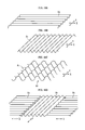
FIG. 16A is an enlarged perspective view showing a grating structure formed in an X-direction, FIG. 16B is an enlarged perspective view showing a grating structure formed in a Y-direction, FIG. 16C is a perspective view showing a complex grating structure in which the grating structure formed in the X-direction and the grating structure formed in the Y-direction are combined with each other, and FIG. 16D is a perspective view showing a grating structure in which the grating structure formed in the X-direction and the grating structure formed in the Y-direction are arranged.
FIG. 17 is a structural diagram showing a grating structure forming apparatus for dividing a pulse laser beam into a plurality of pulse laser beams each having a predetermined time interval to form a grating structure having a direction and a grating structure having another direction during the same process.
DETAILED DESCRIPTION OF THE INVENTION
Hereinafter, the principle for forming a grating structure will be described with reference to the accompanying drawings and then an embodiment of the present invention will be described. FIG. 8A is a schematic cross sectional view showing a parent material having a grating structure on which a DLC coating film is formed by evaporation using a method according to the present invention. FIG. 8B is a schematic cross sectional view showing a parent material having a mirror surface on which a DLC coating film is formed by evaporation using the method. It is recognized that an anchor effect of the DLC coating film in the case shown in FIG. 8A is higher than that in the case shown in FIG. 8B.
FIG. 9 includes a schematic perspective view explaining a mechanism for forming the grating structure and a block diagram showing a process for forming the grating structure. In the schematic perspective view of FIG. 9, when a surface of a parent material 2 is irradiated with a laser beam 1, a p-polarized light component 3 of the incident light interferes with a p-polarized light component 5 of surface scattered light to generate a standing wave 7. Reference numeral 4 denotes an s-polarized light component of the incident light and 6 denotes an s-polarized light component of the surface scattered light.
When a fluence of the incident light is close to a laser processing threshold, an abrasion is caused on only an interference part between the p-polarized light component 3 of the incident light and the p-polarized light component 5 of the surface scattered light traveling along the surface (12). When the abrasion begins to increase surface roughness, an intensity of the surface scattered light increases at the time of next laser irradiation (13). When the abrasion further advances, interference occurs even in the case where positions are separated from each other by a wavelength λ. When the laser irradiation is repeated, the interference occurs at an interval of the wavelength λ of the incident light (14). Therefore, the grating structure is formed (15).
Ripples of the grating structure are grown up to a wavelength order by 10 shots to 300 shots. When laser beam irradiation is performed for 300 shots or more, the ripples become indefinite. Therefore, laser beam scanning is performed with an overlap such that the number of shots emitted to the same position are 10 to 300. Thus, it is possible to widely expand the grating structure on the surface of a specimen. The laser beam scanning may be performed by the movement of a table supporting the parent material 2 or by scanning with a laser beam.
FIG. 10 is a schematic diagram showing a grating structure forming apparatus 20. It should be noted that specific numeral values in the following description are merely examples and thus not particularly limited. A titanium sapphire laser beam 1 (pulse width: 120 fs, center wavelength λ: 800 nm, repetition frequency: 1 kHz, pulse energy E: 0.25 μJ to 400 μJ) is generated by a titanium sapphire laser beam generating apparatus 21. The pulse energy can be adjusted using a ½-wavelength plate 22 and a polarization beam splitter 23. The surface of the parent material 2 located on an X-Y-θ stage 25 is irradiated with the laser beam 1 through a lens (focal length f=100 mm) 24. A resolution of the X-Y-θ stage 25 may be arbitrarily determined, and the resolution is, for example, 2 μm. In order to irradiate the parent material 2 with the laser beam 1 with an overlap, the parent material 2 is moved at a speed of 0.25 mm/s (125 pps) by the X-Y-θ stage 25 to cause an abrasion due to interference between the incident light and scatted light traveling along the surface, with the result that the grating structure is formed.
A scanning speed of the parent material 2 is set based on a spot diameter of the laser beam 1 and the wavelength λ of the laser beam 1. An incident angle θ of the laser beam 1 relative to the parent material 2 is set to 0°. An Si and a Cu tape, each of which has a thickness of 50 μm, are used for the parent material 2. The grating structure obtained by the above-mentioned operation is observed using a laser microscope and an atomic force microscope (AFM).
(Grating Structure of Si)
A surface of an Si substrate serving as the parent material 2 is scanned three times with the laser beam 1 by a plane-convex lens 24 (f=100 mm) at a fluence close to a processing threshold, to form a grating structure. FIGS. 11A and 11B show a grating structure obtained in the case where the scanning direction of the laser beam 1 is in parallel with a polarization direction. FIGS. 12A and 12B show a grating structure obtained in the case where the polarization direction is rotated by 90°. Each of FIGS. 11A and 12A shows the entire state and each of FIGS. 11B and 12B shows an enlarged detail of the formed grating structure. In each of FIGS. 11A and 12A, in order to easily understand three-time scanning, laser irradiation is stopped during the second scanning. Each of the grating structures is formed orthogonal to the polarization direction. A periodic pitch of each of the grating structures is approximately 700 nm which is slightly shorter than the wavelength λ (800 nm) of the laser beam. Large disturbance of an overlapping part in each scanning is not observed.
FIG. 13 shows a grating structure obtained in the case where a laser fluence is reduced to a value closest to the processing threshold to minimally suppress abrasion. A periodic pitch of the grating structure is 795 nm and thus substantially equal to the wavelength λ (center wavelength is 800 nm) of the laser beam.
In order to form the grating structure in a wider area, the laser beam is expanded by a beam expander. Then, a linear laser beam condensed by a cylindrical lens (f=100 mm) is emitted to form a grating structure. As a result, the grating structure is formed corresponding to one-time scanning at a width of 2 mm or more. FIG. 14 shows the formed grating structure. A periodic pitch is 700 nm. As a result, the obtained grating structure is not significantly different from the grating structure formed using the plane-convex lens at the fluence close to the processing threshold (FIGS. 11A and 11B).
When the grating structure obtained using the cylindrical lens is irradiated with white light, spectral performance is observed. In addition, it is recognized that the periodic grating structure having a regular interval is obtained in a wide area.
(Grating Structure of Cu Tape)
When a grating structure is to be formed in the Cu tape using the cylindrical lens (f=100 mm), the grating structure is formed corresponding to one-time scanning at a width of 2 mm or more as in the case of the Si substrate. FIG. 15 shows the grating structure in the CP tape. A periodic pitch of the grating structure is approximately 700 nm. As a result, a difference with the case of the Si substrate is hardly observed.
Even in the case of each parent material except the Si and Cu tape, the grating structure can be formed as in the cases of the Si and Cu tapes.
Therefore, according to the present invention, the surface of the parent material is irradiated with the laser beam and scanning with the irradiation laser beam is performed to form the grating structure. When the polarization direction of the laser beam is set to a Y-direction, a grating structure 8 X can be formed in an X-direction as shown in FIG. 16A. When the polarization direction of the laser beam is set to the X-direction, a grating structure 8 Y can be formed in the Y-direction as shown in FIG. 16B.
The following operation is performed based on the fact that the direction of the grating structure can be changed by adjusting the polarization direction of the laser beam. For example, laser irradiation is performed at the fluence close to the processing threshold and scanning with a laser beam in a direction is performed with an overlap on irradiated areas to form the grating structure 8 X in a direction as shown in FIG. 16A. After that, a relative angle between the surface of the parent material and the polarization direction is adjusted and the laser irradiation is performed so as to be superimposed on the grating structure 8 X at the fluence close to the processing threshold. Scanning with a laser beam is performed with an overlap on irradiated areas to form the grating structure 8 Y in a different direction which is combined with the grating structure 8 X. Therefore, it is possible to obtain a grating structure 8 Z in which the grating structures formed in the plurality of directions are combined with each other. Thus, for example, as shown in FIG. 16C, when the relative angle between the surface of the parent material and the polarization direction of the laser beam is changed by 90° between the time of preceding grating formation and the time of subsequent grating formation, a mesh-shaped grating structure can be formed. When the relative angle between the surface of the parent material and the polarization direction of the laser beam is changed by an arbitrary angle other than 90° between the time of preceding grating formation and the time of subsequent grating formation, an oblique-mesh-shaped grating structure can be formed.
For example, laser irradiation is performed at the fluence close to the processing threshold and scanning with a laser beam in a direction is performed with an overlap on irradiated areas to form the grating structure 8 X in a first direction. After that, the relative angle between the surface of the parent material and the polarization direction is adjusted and the laser irradiation is performed at the fluence close to the processing threshold in a position adjacent to or separated from the grating structure 8 X. Then, scanning with a laser beam is performed with an overlap on irradiated areas, so that the grating structure 8 Y which is adjacent to or separated from the grating structure 8 X previously formed in the first direction can be formed in a second direction different from the first direction, as shown in FIG. 16D. Therefore, when the relative angle between the surface of the parent material and the polarization direction of the laser beam is changed by 90° between the time of preceding grating formation and the time of subsequent grating formation, the grating structure 8 X formed in the X-direction and the grating structure 8 Y formed in the Y-direction can be arranged. When the relative angle between the surface of the parent material and the polarization direction of the laser beam is changed by an arbitrary angle other than 90° between the time of preceding grating formation and the time of subsequent grating formation, the grating structures can be arranged in different directions.
The following operation is performed based on the above-mentioned fact that the direction of the grating structure can be changed by adjusting the polarization direction of the laser beam. The grating structure in which the grating structures formed in the plurality of directions are combined with each other as shown in FIG. 16C can be obtained using a laser irradiation apparatus 40 shown in FIG. 17 by a single process. In the grating structure forming apparatus 40 shown in FIG. 17, a laser beam L0 generated by a titanium sapphire laser beam generating device 41 is totally reflected by a mirror 42 and divided into laser beams L1 and L2 by a half mirror 43. The laser beam L1 is totally reflected by each of mirrors 44 and 45. In contrast, the laser L2 is optically delayed by an optical delay portion 46. The optical delay portion 46 includes mirrors 47 and 48. Laser beams L3 and L4 obtained by polarizing the laser beams L1 and L2 in predetermined directions by polarization devices 49 and 50, respectively, are applied to a half mirror 51. The polarized laser beams L3 and L4 are superimposed on each other by the half mirror 51 and a surface of a parent material 54 mounted on an X-Y table 53 is irradiated therewith through a lens 52. Therefore, the surface of the parent material 54 can be irradiated with the laser beams L3 and L4 at fluences close to processing thresholds of a plurality of pulses with different polarization directions at predetermined time intervals. When scanning is performed with an overlap on irradiated areas, the grating structure 8 Z in which the grating structures formed in the plurality of directions are combined with each other as shown in FIG. 16C can be obtained at a time.
For example, the surface of the parent material is irradiated with the laser beams L3 and L4 at the fluences close to the processing thresholds of the plurality of pulses whose polarization directions are different from each other by 90° at predetermined time intervals and the scanning is performed with an overlap on the irradiated areas. As a result, the mesh-shaped grating structure 8 Z in which the grating structure 8 X formed in the X-direction and the grating structure 8 Y formed in the Y-direction different from the X-direction by 90° are combined with each other as shown in FIG. 16C can be obtained by a single process. In addition, the surface of the parent material is irradiated with the laser beams at fluences close to processing thresholds of a plurality of pulses whose polarization directions are different from each other by an arbitrary angle other than 90° at the predetermined time intervals and scanning is performed with an overlap on irradiated areas. As a result, an oblique-mesh-shaped grating structure in which grating structures intersect with each other at the arbitrary angle other than 90° can be formed. In a matter of course, the angle can be 0°, that is, two polarization directions are aligned with each other.
Next, a change in surface characteristic of the parent material which is caused by the above-mentioned grating structure will be described. The SUS304 substrate is used as the parent material whose surface characteristic is changed. A titanium sapphire laser beam of ultra-short pulse (for example, pulse width is 120 fs, center frequency is 800 nm, repetition frequency is 1 kHz, and pulse energy is 140 μJ/pulse) is used as an irradiation laser beam. The laser beam is expanded by a beam expander. Then, the laser beam condensed by a cylindrical lens to irradiate the surface of the SUS304 substrate therewith. Scanning is performed at a scanning speed of 0.5 mm/s with an overlap on irradiated portions. As a result, a grating structure is formed at a periodic pitch of 0.7 μm and a depth of 0.2 μm. It is apparent from results obtained by a pin-on-disk test and a scratch test that, when the SUS 304 substrate (parent material) in which the grating structure is formed is coated with a DLC coating film, the adhesion to the parent material is significantly improved. In addition, it is observed that the shape of the grating structure is left in the surface of the DLC coating film.
According to the method for enhancing adhesion of a thin film in the present invention, the grating structure is formed in the surface of the parent material in the spontaneous manner and the solid thin film is formed on the grating structure. Therefore, the peeling of the solid thin film, the DLC coating film in particular, is prevented by, for example, a strong anchor effect caused by the grating structure. When the shape of the grating structure formed in the parent material is left in the upper surface of the solid thin film, surface functions such as a function for reducing friction and wear which are caused by a shape, a function for suppressing adhesion of fine particles, and cell sensitivity can be exhibited in conjunction with a function of the solid thin film.
The method according to the present invention is useful to improve the adhesion strength of the solid thin film in all fields. In particular, it is useful to improve the tribology characteristics.

Claims (5)

The invention claimed is:
1. A method for enhancing adhesion of a thin film, said method comprising:
irradiating a surface of a parent material with a laser beam polarized in one predetermined direction at a fluence (energy density) close to a processing threshold;
performing a scan with the laser beam on the surface of the parent material with an overlap such that the total number of shots of the laser beam irradiated on the same position of the surface of the parent material is within a range of 10 to 300, so as to cause ablation on the surface of the parent material at a region where interference occurs between a polarization light component of a surface scattered light traveling along the surface of the parent material, and thereby to form a grating structure spontaneously on the surface of the parent material in one predetermined direction orthogonal to a polarization direction of the incident light of the laser beam; and
forming a solid thin film on the grating structure of the surface of the parent material.
2. The method for enhancing adhesion of a thin film according to claim 1, further comprising condensing the laser beam by a cylindrical lens to form the grating structure in a wide area.
3. The method for enhancing adhesion of a thin film according to claim 1, wherein the solid thin film contains diamond-like carbon (DLC).
4. The method for enhancing adhesion of a thin film according to claim 1, wherein the solid thin film contains hydroxyapatite.
5. The method for enhancing adhesion of a thin film according to claim 1, wherein a shape of the grating structure formed on the surface of the parent material is left in an upper surface of the solid thin film to add a surface function caused by the shape to the solid thin film.
US11/630,906 2004-09-06 2004-09-06 Method for enhancing adhesion of thin film Active 2029-11-29 US8728585B2 (en)

Applications Claiming Priority (1)

Application Number Priority Date Filing Date Title
PCT/JP2004/013277 WO2006027850A1 (en) 2004-09-06 2004-09-06 Method for enhancing adhesion of thin film

Publications (2)

Publication Number Publication Date
US20080124486A1 US20080124486A1 (en) 2008-05-29
US8728585B2 true US8728585B2 (en) 2014-05-20

Family

ID=36036147

Family Applications (1)

Application Number Title Priority Date Filing Date
US11/630,906 Active 2029-11-29 US8728585B2 (en) 2004-09-06 2004-09-06 Method for enhancing adhesion of thin film

Country Status (4)

Country Link
US (1) US8728585B2 (en)
EP (1) EP1788115A4 (en)
JP (1) JP4440270B2 (en)
WO (1) WO2006027850A1 (en)

Cited By (1)

* Cited by examiner, † Cited by third party
Publication number Priority date Publication date Assignee Title
US10774003B2 (en) 2014-09-11 2020-09-15 National Institute Of Advanced Industrial Science And Technology Surface structure forming method for zirconia-based ceramics, and zirconia-based ceramics

Families Citing this family (15)

* Cited by examiner, † Cited by third party
Publication number Priority date Publication date Assignee Title
JP5111961B2 (en) * 2007-07-09 2013-01-09 キヤノンマシナリー株式会社 Sliding surface structure
FR2921012A1 (en) * 2007-09-13 2009-03-20 Advanced Track And Trace Sa Surface marking method for e.g. document, involves determining image representing information, and marking surface with polarized laser beam to form oriented nanostructures representing image on surface
JP2014055091A (en) * 2012-09-13 2014-03-27 Osaka Univ Method for producing group iii-v compound crystal, method for producing seed crystals formed substrate, group iii-v compound crystal, semiconductor device, group iii-v compound crystal producing apparatus, seed crystals formed substrate producing apparatus
JP6199655B2 (en) * 2013-08-07 2017-09-20 アイシン精機株式会社 Composite molded product
JP6479414B2 (en) * 2013-11-05 2019-03-06 国立研究開発法人産業技術総合研究所 Medical device material manufacturing method and medical device material
US10189117B2 (en) 2013-12-31 2019-01-29 The United States Of America, As Represented By The Secretary Of The Navy Adhesion improvement via material nanostructuring or texturizing
US10106880B2 (en) 2013-12-31 2018-10-23 The United States Of America, As Represented By The Secretary Of The Navy Modifying the surface chemistry of a material
JP6392130B2 (en) * 2015-01-20 2018-09-19 キヤノンマシナリー株式会社 Manufacturing method of sliding surface structure
JP6590399B2 (en) * 2015-04-24 2019-10-16 国立研究開発法人産業技術総合研究所 Medical device material manufacturing method and medical device material
JP6573102B2 (en) * 2015-04-27 2019-09-11 国立研究開発法人産業技術総合研究所 Medical device material and manufacturing method thereof
JP6515387B2 (en) * 2015-09-15 2019-05-22 日本製鉄株式会社 Carbide tool and method of manufacturing the same
TWI581488B (en) * 2015-10-13 2017-05-01 Metal Ind Res & Dev Ct Method for manufacturing negative electrode plate of secondary battery
CN106838076B (en) * 2016-12-13 2020-01-17 杭州电子科技大学 Brake disc with wear-resistant hydroxyapatite coating and manufacturing method thereof
JP7250408B2 (en) * 2019-07-27 2023-04-03 林 美子 Hydrogen conduit structure and fabrication method
WO2023172771A2 (en) * 2022-03-11 2023-09-14 Aspen Hybrid Technology Systems Surface treatment methods and systems, and surface-treated articles

Citations (10)

* Cited by examiner, † Cited by third party
Publication number Priority date Publication date Assignee Title
JPH0557464A (en) * 1991-09-02 1993-03-09 Nikon Corp Laser beam machine
US5569399A (en) * 1995-01-20 1996-10-29 General Electric Company Lasing medium surface modification
US5709907A (en) * 1995-07-14 1998-01-20 Kennametal Inc. Method of making coated cutting tools
US5776355A (en) * 1996-01-11 1998-07-07 Saint-Gobain/Norton Industrial Ceramics Corp Method of preparing cutting tool substrate materials for deposition of a more adherent diamond coating and products resulting therefrom
JPH11310868A (en) 1998-04-30 1999-11-09 Toyota Central Res & Dev Lab Inc Production of coated member
US6010283A (en) * 1997-08-27 2000-01-04 Kennametal Inc. Cutting insert of a cermet having a Co-Ni-Fe-binder
US20020190435A1 (en) * 2001-01-31 2002-12-19 O'brien James N. Laser segmented cutting
JP2003211400A (en) 2002-01-22 2003-07-29 Japan Science & Technology Corp Refining method using ultra-short pulse laser and workpiece therefor
JP2003253424A (en) 2002-03-01 2003-09-10 Shigeki Mototsu Hydroxyapatite film coating material and manufacturing method thereof
WO2004035255A1 (en) 2002-09-27 2004-04-29 Nec Machinery Corporation Cyclic structure formation method and surface treatment method

Family Cites Families (4)

* Cited by examiner, † Cited by third party
Publication number Priority date Publication date Assignee Title
US5072091A (en) * 1989-04-03 1991-12-10 The Local Government Of Osaka Prefecture Method and apparatus for metal surface process by laser beam
JP3448884B2 (en) 1992-12-15 2003-09-22 日本精工株式会社 Artificial diamond coating
US5558789A (en) 1994-03-02 1996-09-24 University Of Florida Method of applying a laser beam creating micro-scale surface structures prior to deposition of film for increased adhesion
FR2801234A1 (en) 1999-06-22 2001-05-25 Gaillard Jacques Pretreatment of cutting blades for tungsten carbide cutting tools to be diamond coated by chemical vapour deposition (CVD)

Patent Citations (10)

* Cited by examiner, † Cited by third party
Publication number Priority date Publication date Assignee Title
JPH0557464A (en) * 1991-09-02 1993-03-09 Nikon Corp Laser beam machine
US5569399A (en) * 1995-01-20 1996-10-29 General Electric Company Lasing medium surface modification
US5709907A (en) * 1995-07-14 1998-01-20 Kennametal Inc. Method of making coated cutting tools
US5776355A (en) * 1996-01-11 1998-07-07 Saint-Gobain/Norton Industrial Ceramics Corp Method of preparing cutting tool substrate materials for deposition of a more adherent diamond coating and products resulting therefrom
US6010283A (en) * 1997-08-27 2000-01-04 Kennametal Inc. Cutting insert of a cermet having a Co-Ni-Fe-binder
JPH11310868A (en) 1998-04-30 1999-11-09 Toyota Central Res & Dev Lab Inc Production of coated member
US20020190435A1 (en) * 2001-01-31 2002-12-19 O'brien James N. Laser segmented cutting
JP2003211400A (en) 2002-01-22 2003-07-29 Japan Science & Technology Corp Refining method using ultra-short pulse laser and workpiece therefor
JP2003253424A (en) 2002-03-01 2003-09-10 Shigeki Mototsu Hydroxyapatite film coating material and manufacturing method thereof
WO2004035255A1 (en) 2002-09-27 2004-04-29 Nec Machinery Corporation Cyclic structure formation method and surface treatment method

Non-Patent Citations (11)

* Cited by examiner, † Cited by third party
Title
A. E. Siegman, P. M. Fauchet, "Stimulated Wood's Anomalies on Laser-illuminated Surfaces", IEEE J. Quantum Electron, QE-20, 8 (1986), pp. 1384-1403.
Akio Motoi, Seiji Kataoka and Kazuo Morikawa, "An Evaluation Method for the Adhesion of DLC Coated Tools Intended for Plastic Forming", Bulletin of Tokyo Metropolitan Industrial Technology Research Institute, 6, 2003.
H. Hiraoka and M. Sendova, "Laser-induced Sub-half-micrometer Periodic Structure on Polymer Surfaces", App. Phys. Lett., 64, 5, (1994) pp. 563-565.
Hiroshi Sawada, Kosuke Kawahara, Takafumi Ninomiya, Atsunobu Mori and Kou Kurosawa, "Effect of Precise Periodic Structures with Femtosecond-laser on Tribological Characteristics under Sliding Tests", Journal of the Japan Society for Precision Engineering, 70, 1 (2004), pp. 113-137.
Hiroshi Sawada, Kosuke Kawahara, Takafumi Ninomiya, Kou Kurosawa and Atsushi Yokotani, "Precise Periodic Structuring with Femtosecond-laser", Journal of the Japan Society for Precision Engineering, 69, 4 (2003), pp. 554-558.
International Search Report mailed Jan. 25, 2005 for International Application No. PCT/JP2004/013277.
M. Bolle and S. Lazare, "Submicron Periodic Structures Provided on Polymer Surfaces with Polarized Excimer Laser Ultraviolet Radiation", Appl. Phys. Lett., 60 6 (1992), pp. 674-676.
N. Yasumaru, K. Miyazaki and J. Kiuchi, "Femtosecond-laser-induced Nanostructure Formed on Hard Thin Films of TiN and DLC", Appl. Phys. A 76, pp. 983-985, 2003.
P. E. Dyer and R. J. Farley, "Periodic Surface Structures in the Excimer Laser Ablative Etching of Polymers", Appl. Phys. Lett., 57, 8 (1990), pp. 765-767.
Takeshi Furuno, Atsunobu Mori, Norio Tagawa, Hiroshi Sawada, "Effects of Precise Periodic Structures on Fatigue Resistance of Rolling-sliding contact surface", Proceedings of JAST Tribology Conference, Tokyo, May 2004, pp. 119-120.
Yukimasa Minami and Koichi Toyoda, "Incident-Angle Dependency of Laser-induced Surface Ripples on Metals and Semiconductors", Review of Laser Engineering, 28, 12, (2000), pp. 824-828.

Cited By (1)

* Cited by examiner, † Cited by third party
Publication number Priority date Publication date Assignee Title
US10774003B2 (en) 2014-09-11 2020-09-15 National Institute Of Advanced Industrial Science And Technology Surface structure forming method for zirconia-based ceramics, and zirconia-based ceramics

Also Published As

Publication number Publication date
JPWO2006027850A1 (en) 2008-05-08
US20080124486A1 (en) 2008-05-29
EP1788115A1 (en) 2007-05-23
EP1788115A4 (en) 2013-02-27
WO2006027850A1 (en) 2006-03-16
JP4440270B2 (en) 2010-03-24

Similar Documents

Publication Publication Date Title
US8728585B2 (en) Method for enhancing adhesion of thin film
EP1586405B1 (en) Method of forming a periodic structure on a material surface
Raciukaitis et al. Use of high repetition rate and high power lasers in microfabrication: How to keep the efficiency high?
JP2006212646A (en) Method for preparing periodic structure
Kononenko et al. Laser ablation and micropatterning of thin TiN coatings
Beausoleil et al. Deep and high precision cutting of alumina ceramics by picosecond laser
JP4263865B2 (en) Fine processing method using ultra-short pulse laser and processed product
JP2007162045A (en) Sliding material and its production method
Won et al. Effects of laser parameters on morphological change and surface properties of aluminum alloy in masked laser surface texturing
Lasagni et al. Direct fabrication of periodic structures on surfaces: laser interference patterning as new scalable industrial tool
Bonse et al. Structuring of thin films by ultrashort laser pulses
Roessler et al. Protecting Sub-Micrometer Surface Features in Polymers from Mechanical Damage Using Hierarchical Patterns.
Rathmann et al. Influence of laser hardening on laser induced periodic surface structures on steel substrates
Fang et al. Fabrication of interference textures on cemented carbides using nanosecond and femtosecond laser pulses
Teicher et al. Laser Structuring with DLIP technology of tungsten carbide with different binder content
Ashkenasi et al. Material processing of dielectrics with femtosecond lasers
Vu et al. Investigating the effect of pulsed fiber laser parameters on the roughness of aluminium alloy and steel surfaces in cleaning processes
Butler-Smith et al. A comparison of the tactile friction and cutting performance of textured scalpel blades modified by Direct Laser Writing and Direct Laser Interference Patterning processes
Schulze et al. Precise ablation milling with ultrashort pulsed Nd: YAG lasers by optical and acoustical process control
Klimpel et al. The influence of the shielding gas on the properties of a laser-melted surface of austenitic stainless steel
Haehnel et al. Production of microstructures in wide-band-gap and organic materials using pulsed laser ablation at 157 nm wavelength
JP2004188436A (en) Method for machining fine inclined face
Liu et al. Polarization effects on laser-inscribed angled micro-structures
Romano et al. Laser surface microstructuring to improve tribological systems
Gupta et al. Design of micro-scale periodic surface textures by pulsed laser melting and its influence on wettability

Legal Events

Date Code Title Description
AS Assignment

Owner name: CANON MACHINERY INC., JAPAN

Free format text: ASSIGNMENT OF ASSIGNORS INTEREST;ASSIGNORS:SAWADA, HIROSHI;KAWAHARA, KOSUKE;REEL/FRAME:020155/0756

Effective date: 20070116

STCF Information on status: patent grant

Free format text: PATENTED CASE

MAFP Maintenance fee payment

Free format text: PAYMENT OF MAINTENANCE FEE, 4TH YEAR, LARGE ENTITY (ORIGINAL EVENT CODE: M1551)

Year of fee payment: 4

MAFP Maintenance fee payment

Free format text: PAYMENT OF MAINTENANCE FEE, 8TH YEAR, LARGE ENTITY (ORIGINAL EVENT CODE: M1552); ENTITY STATUS OF PATENT OWNER: LARGE ENTITY

Year of fee payment: 8