EP0841587B1 - Mach-Zehnder optischer Modulator mit einstellbarem Chirp und Verfahren zur Erzeugung einstellbaren Chirps - Google Patents
Mach-Zehnder optischer Modulator mit einstellbarem Chirp und Verfahren zur Erzeugung einstellbaren Chirps Download PDFInfo
- Publication number
- EP0841587B1 EP0841587B1 EP97308615A EP97308615A EP0841587B1 EP 0841587 B1 EP0841587 B1 EP 0841587B1 EP 97308615 A EP97308615 A EP 97308615A EP 97308615 A EP97308615 A EP 97308615A EP 0841587 B1 EP0841587 B1 EP 0841587B1
- Authority
- EP
- European Patent Office
- Prior art keywords
- electric field
- arm
- arms
- phase difference
- chirp
- Prior art date
- Legal status (The legal status is an assumption and is not a legal conclusion. Google has not performed a legal analysis and makes no representation as to the accuracy of the status listed.)
- Expired - Lifetime
Links
Images


Classifications
-
- G—PHYSICS
- G02—OPTICS
- G02F—OPTICAL DEVICES OR ARRANGEMENTS FOR THE CONTROL OF LIGHT BY MODIFICATION OF THE OPTICAL PROPERTIES OF THE MEDIA OF THE ELEMENTS INVOLVED THEREIN; NON-LINEAR OPTICS; FREQUENCY-CHANGING OF LIGHT; OPTICAL LOGIC ELEMENTS; OPTICAL ANALOGUE/DIGITAL CONVERTERS
- G02F1/00—Devices or arrangements for the control of the intensity, colour, phase, polarisation or direction of light arriving from an independent light source, e.g. switching, gating or modulating; Non-linear optics
- G02F1/01—Devices or arrangements for the control of the intensity, colour, phase, polarisation or direction of light arriving from an independent light source, e.g. switching, gating or modulating; Non-linear optics for the control of the intensity, phase, polarisation or colour
- G02F1/21—Devices or arrangements for the control of the intensity, colour, phase, polarisation or direction of light arriving from an independent light source, e.g. switching, gating or modulating; Non-linear optics for the control of the intensity, phase, polarisation or colour by interference
- G02F1/225—Devices or arrangements for the control of the intensity, colour, phase, polarisation or direction of light arriving from an independent light source, e.g. switching, gating or modulating; Non-linear optics for the control of the intensity, phase, polarisation or colour by interference in an optical waveguide structure
- G02F1/2257—Devices or arrangements for the control of the intensity, colour, phase, polarisation or direction of light arriving from an independent light source, e.g. switching, gating or modulating; Non-linear optics for the control of the intensity, phase, polarisation or colour by interference in an optical waveguide structure the optical waveguides being made of semiconducting material
-
- B—PERFORMING OPERATIONS; TRANSPORTING
- B82—NANOTECHNOLOGY
- B82Y—SPECIFIC USES OR APPLICATIONS OF NANOSTRUCTURES; MEASUREMENT OR ANALYSIS OF NANOSTRUCTURES; MANUFACTURE OR TREATMENT OF NANOSTRUCTURES
- B82Y20/00—Nanooptics, e.g. quantum optics or photonic crystals
-
- G—PHYSICS
- G02—OPTICS
- G02F—OPTICAL DEVICES OR ARRANGEMENTS FOR THE CONTROL OF LIGHT BY MODIFICATION OF THE OPTICAL PROPERTIES OF THE MEDIA OF THE ELEMENTS INVOLVED THEREIN; NON-LINEAR OPTICS; FREQUENCY-CHANGING OF LIGHT; OPTICAL LOGIC ELEMENTS; OPTICAL ANALOGUE/DIGITAL CONVERTERS
- G02F1/00—Devices or arrangements for the control of the intensity, colour, phase, polarisation or direction of light arriving from an independent light source, e.g. switching, gating or modulating; Non-linear optics
- G02F1/01—Devices or arrangements for the control of the intensity, colour, phase, polarisation or direction of light arriving from an independent light source, e.g. switching, gating or modulating; Non-linear optics for the control of the intensity, phase, polarisation or colour
- G02F1/21—Devices or arrangements for the control of the intensity, colour, phase, polarisation or direction of light arriving from an independent light source, e.g. switching, gating or modulating; Non-linear optics for the control of the intensity, phase, polarisation or colour by interference
- G02F1/225—Devices or arrangements for the control of the intensity, colour, phase, polarisation or direction of light arriving from an independent light source, e.g. switching, gating or modulating; Non-linear optics for the control of the intensity, phase, polarisation or colour by interference in an optical waveguide structure
-
- G—PHYSICS
- G02—OPTICS
- G02F—OPTICAL DEVICES OR ARRANGEMENTS FOR THE CONTROL OF LIGHT BY MODIFICATION OF THE OPTICAL PROPERTIES OF THE MEDIA OF THE ELEMENTS INVOLVED THEREIN; NON-LINEAR OPTICS; FREQUENCY-CHANGING OF LIGHT; OPTICAL LOGIC ELEMENTS; OPTICAL ANALOGUE/DIGITAL CONVERTERS
- G02F1/00—Devices or arrangements for the control of the intensity, colour, phase, polarisation or direction of light arriving from an independent light source, e.g. switching, gating or modulating; Non-linear optics
- G02F1/01—Devices or arrangements for the control of the intensity, colour, phase, polarisation or direction of light arriving from an independent light source, e.g. switching, gating or modulating; Non-linear optics for the control of the intensity, phase, polarisation or colour
- G02F1/015—Devices or arrangements for the control of the intensity, colour, phase, polarisation or direction of light arriving from an independent light source, e.g. switching, gating or modulating; Non-linear optics for the control of the intensity, phase, polarisation or colour based on semiconductor elements having potential barriers, e.g. having a PN or PIN junction
- G02F1/017—Structures with periodic or quasi periodic potential variation, e.g. superlattices, quantum wells
- G02F1/01708—Structures with periodic or quasi periodic potential variation, e.g. superlattices, quantum wells in an optical wavequide structure
-
- G—PHYSICS
- G02—OPTICS
- G02F—OPTICAL DEVICES OR ARRANGEMENTS FOR THE CONTROL OF LIGHT BY MODIFICATION OF THE OPTICAL PROPERTIES OF THE MEDIA OF THE ELEMENTS INVOLVED THEREIN; NON-LINEAR OPTICS; FREQUENCY-CHANGING OF LIGHT; OPTICAL LOGIC ELEMENTS; OPTICAL ANALOGUE/DIGITAL CONVERTERS
- G02F2201/00—Constructional arrangements not provided for in groups G02F1/00 - G02F7/00
- G02F2201/12—Constructional arrangements not provided for in groups G02F1/00 - G02F7/00 electrode
- G02F2201/126—Constructional arrangements not provided for in groups G02F1/00 - G02F7/00 electrode push-pull
-
- G—PHYSICS
- G02—OPTICS
- G02F—OPTICAL DEVICES OR ARRANGEMENTS FOR THE CONTROL OF LIGHT BY MODIFICATION OF THE OPTICAL PROPERTIES OF THE MEDIA OF THE ELEMENTS INVOLVED THEREIN; NON-LINEAR OPTICS; FREQUENCY-CHANGING OF LIGHT; OPTICAL LOGIC ELEMENTS; OPTICAL ANALOGUE/DIGITAL CONVERTERS
- G02F2203/00—Function characteristic
- G02F2203/20—Intrinsic phase difference, i.e. optical bias, of an optical modulator; Methods for the pre-set thereof
-
- G—PHYSICS
- G02—OPTICS
- G02F—OPTICAL DEVICES OR ARRANGEMENTS FOR THE CONTROL OF LIGHT BY MODIFICATION OF THE OPTICAL PROPERTIES OF THE MEDIA OF THE ELEMENTS INVOLVED THEREIN; NON-LINEAR OPTICS; FREQUENCY-CHANGING OF LIGHT; OPTICAL LOGIC ELEMENTS; OPTICAL ANALOGUE/DIGITAL CONVERTERS
- G02F2203/00—Function characteristic
- G02F2203/25—Frequency chirping of an optical modulator; Arrangements or methods for the pre-set or tuning thereof
Definitions
- This invention relates to a multi-quantum-well Mach-Zehnder phase modulator with a built-in phase shift and more particularly to such a device having separate control means for generating a modulated optical signal having either positive or negative frequency chirp with a high extinction ratio for high quality transmission over either dispersion shifted fiber or non-dispersion shifter fiber.
- Semiconductor lasers and particularly lasers fabricated from selected III-V compounds such as InGaAsP/InP can be tailored to generate an optical signal at the appropriate wavelength.
- Modulated lasers however, have spectral broadening due in part to a wavelength shift or chirp brought about by the modulation.
- the pulse broadening is a result of a wavelength shift to shorter wavelengths (blue shift) at the rising edge of a modulating pulse and a wavelength shift to longer wavelengths (red shift) at the falling edge of the pulse. This is known as positive frequency chirp.
- Propagating through a non-dispersion shifted fiber a pulse with positive frequency chirp is broadened because the rising edge moves faster and the falling edge moves slower. This frequency chirp can be quite large for directly modulated lasers and, as a result, the span between repeaters in an optical fiber network operating at high speed and utilizing such devices as transmitters is necessarily low.
- An alternative to directly modulated lasers is an electro-optical modulator which, in conjunction with a C.W. operated laser, offers the promise of a modulated signal with controllable chirp.
- An electro-optical modulator of particular interest is the Mach-Zehnder phase modulator operating as an interferometer.
- Prior art Mach-Zehnder modulators are commonly fabricated in lithium niobate (LiNbO 3 ) with titanium (Ti) diffused waveguides. The frequency chirp characteristics of such devices have been studied and reported in the literature.
- Okiyama et al (“10 Gb/s Transmission in Large Dispersion Fiber Using Ti:LiNbO 3 Mach-Zehnder Modulator", Conf. Integrated Optics and Optical Fiber Communication, Kobe, Japan, 1989), reported that Mach-Zehnder modulators could modulate a CW laser at bit rates up to 10 Gb/s although frequency chirp was noted.
- Mach-Zehnder modulators have been fabricated in III-V material such as InP with multi-quantum-wells of InP/InGaAsP in the guided regions.
- III-V material such as InP with multi-quantum-wells of InP/InGaAsP in the guided regions.
- Rolland et al 10 Gb/s 120km Normal Fiber Transmission Experiment Using a 1.56 ⁇ m Multi-Quantum-Well InP/InGaAsP Mach-Zehnder Modulator", Conf. Optical Fiber Communication, San Jose, Ca. 1993
- some frequency chirp regulation is possible.
- a Mach-Zehnder phase modulator is based on an interferometric configuration which converts phase modulation into intensity modulation.
- the differential phase shift between the two arms of the modulator equals ⁇
- the antisymmetric mode is excited near the output and is subsequently diffracted out of the single mode waveguide. This is the 'off' or logic '0' state.
- the fundamental mode is excited and propagates with little loss to the output. This is the 'on' or logic ⁇ 1' state.
- the ability to control the frequency chirp of Mach-Zehnder modulators by varying the drive voltage to the arms or by a power splitting ratio has made them well suited for multi-gigabit long distance optical fiber transmission.
- the drive voltage which controls the differential phase shift is conventionally supplied to one arm (single arm drive) or to both arms (dual arm drive). This relationship will be discussed in greater detail later. In any event single arm drive conditions require a larger operating voltage than dual arm drive, while the dual arm driven with equal push-pull voltage for a LiNbO 3 modulator gives substantially zero chirp.
- III-V Mach-Zehnder modulator and a LiNbO 3 Mach-Zehnder
- absorption increases with voltage applied to the arms while absorption is not present in the latter.
- the amount of absorption in the III-V device depends on how close the operating wavelength is to the exciton peak of the multi-quantum-well material.
- LiNbO 3 Mach-Zehnder and a III-V device having a MQW is that the latter shows a non-linear phase change as a function of bias voltage. The non-linear phase change is used to advantage in the present invention, while the disadvantage of absorption is minimized.
- the Mach-Zehnder modulator converts phase modulation into intensity modulation it is important that the ratio between the 'on' state and 'off' state is relatively high.
- This ratio also known as the extinction ratio (ER) is a measure of the signal intensity against background noise. Consequently, a high extinction ratio also permits a greater span between repeaters in a transmission network.
- negative chirp is advantageous for data transmission over non-dispersion-shifted optical fibre.
- the amount of negative chirp applied is, of course, important as too much will also have adverse affects on the pulse train.
- the present invention utilizes the phase shift by optical path length as described in the prior application and adds to it means to further adjust the phase by an electric field, whereby a configurable chirp is obtained.
- MQW multi-quantum-well
- MZ Mach-Zehnder
- a multi-quantum-well Mach-Zehnder phase modulator for selectively generating positive and negative frequency chirp in an optical signal of a known free-space wavelength.
- the modulator comprises an asymmetric input y-junction waveguide coupler having an input waveguide for receiving the optical signal, as well as first and second input branch waveguides and an asymmetric output y-junction waveguide coupler having an output waveguide for delivering the modulated optical signal and first and second output branch waveguides.
- the modulator also has a first interferometric arm between first branch waveguides of the input and output y-junction couplers defining a first optical path and a second interferometric arm between second branch waveguides of the input and output y-junction couplers defining a second optical path, one of the path lengths being greater than the other by a distance which generates a fixed phase difference of ⁇ or an integral odd multiple of ⁇ at the known wavelength and zero bias. Electrodes are provided on the first and second interferometric arms for applying an electric field to modulate the effective phase difference between the arms. A control electrode is provided on one of the arms for selectively applying a control electric field to modulate the phase difference between the arms. With no electric field on the control electrode a negative frequency chirp is generated and with a control electric field on the arm equal to the field required to generate a phase difference of ⁇ , or an integral odd multiple of ⁇ , a positive frequency chirp is generated.
- the fixed phase difference generated by the differential in length between the two interferometric arms is ⁇ /2.
- a control electrode is provided on each of the interferometric arms for receiving a control electric field.
- the control field is such that a further phase difference of ⁇ /2 is selectively applied to one or other interferometric arms resulting in either no phase difference or a selective phase difference of ⁇ .
- positive or negative frequency chirp is generated by the phase modulator depending on which arm is supplied with the control electric field.
- a method of selectively generating positive and negative frequency chirp in an optical signal of known free-space wavelength comprising the steps of: (a) coupling the optical signal to a multi-quantum-well Mach-Zehnder phase modulator having an asymmetric input y-junction coupler and an asymmetric output y-junction coupler with first and second interferometric arms therebetween defining first and second optical paths, one of the paths being longer than the other by a length which generates a fixed phase difference of ⁇ or an integral odd multiple of ⁇ at the known wavelength and zero bias; first and second electrodes on respective arms for receiving a biasing and modulating electric field in order to adjust the effective phase differential between the respective arms, and a control electrode on one of the arms; (b) supplying an electric field to each of the first and second electrodes in an equal push-pull relationship, the magnitude of the electric field being selected to produce a phase difference of ⁇ or an integral odd multiple of ⁇ ; and (c
- the phase difference created by the length differential between the interferometric arms is selected to be ⁇ /2.
- each of the arms has a control electrode and a control electric field equal to the field required to generate an effective phase difference of ⁇ /2 is selectively applied to each arm whereby a control electric field to one arm generates a negative frequency chirp and a control electric field to the other arm generates a positive frequency chirp.
- a highly desirable feature of an external light modulator is the ability to generate a signal with an adjustable frequency chirp.
- Mach-Zehnder (MZ) III-V multi-quantum-well (MQW) modulators are thus increasingly attractive relative to other modulator designs because of their adjustable frequency chirp, low drive voltage, small size, long term reliability and potential for integration with laser sources.
- MZ Mach-Zehnder
- MQW multi-quantum-well
- the larger phase change in a push-pull configuration occurs in the more deeply DC-biased arm because of the non-linear nature of the quantum confined Stark effect.
- the total optical field at the output of the modulator can be regarded to a first approximation as a weighted summation of the optical field from the two separate arms. The weight factors depend on the power splitting ratio of the two y-junctions and the photo-absorption in the modulation section.
- FIGURE 1A illustrates the push-pull drive conditions for obtaining positive chirp in a conventional (i.e., equal arm lengths) III-V MQW MZ modulator.
- the device driven in a push-pull configuration, is switched from an "off” to an "on” state.
- the phase of the optical field in Arm 1 is thus decreased when the device is switched from an "off” to "on” state so that the change in frequency ⁇ 1 >0 and consequently the optical field is blue-shifted.
- ⁇ 0 ⁇ 0 and the optical field is red-shifted in Arm 0.
- FIGURE 1B illustrates the bias voltage relationship in the situation in which Arm 1 has the greater optical power but is biased from 0 to V ⁇ /2. This does generate negative chirp albeit of poor quality. Further, the extinction ratio is also low.
- FIGURE 2A illustrates the relationship for both arms of a ⁇ phase shifted III-V MQW MZ modulator as described in the aforementioned 08/612,555 application.
- the device is switched on when both arms reach the pull-state.
- the phase of the optical field in Arm 1 is thus decreased when the device is switched from the "off” to "on” state so that ⁇ 1 ⁇ 0, red-shifting the optical field in Arm 1.
- FIGURE 2B shows the push-pull drive conditions necessary to obtain positive chirp with a ⁇ phase shifted MZ modulator.
- FIGURE 1A shows good positive chirp and a good extinction ratio while FIGURE 2A shows good negative chirp and a good extinction ratio.
- the present invention obtains both of these results in a single modulator.
- FIGURE 3 is a simplified plan drawing of the structure of the Mach-Zehnder modulator.
- the device is formed in III-V material such as InP/InGaAsP having multi-quantum-wells.
- III-V material such as InP/InGaAsP having multi-quantum-wells.
- prior U.S. Application 08/612,555 identified herein.
- the optical path length through arm 1 of the interferometer is longer than the path length through arm 0 by the distance equivalent to ⁇ or an integral odd multiple thereof at the operating free space wavelength of the device.
- the optical path through arm 1 is .24 ⁇ m longer than through arm 0 for a ⁇ phase shift.
- the modulator structure 18 includes asymmetric input y-junction waveguide 22 and asymmetric output y-junction waveguide 20.
- Branch arms 24,26 are optically parallel and join the y-junction couplers as shown.
- Each branch arm 24,26 has two separated contact pads 28,30 and 32,34 respectively.
- Pads 28, 32 have bonding zones 36,38, and 44,46 respectively for connection to power sources and impedance termination as is well known in the art.
- bias and modulation voltage in push-pull mode is supplied to pads 28,32 while pad 34 is for supplying control voltage as better shown in FIGURES 4A and 4B.
- FIGURES 4B shows the same relationship as that shown in FIGURE 2A for good extinction ratio (ER) and good negative chirp.
- FIGURE 4A The conditions shown in FIGURE 4A can be equated to the conditions set out in FIGURE 1A for good ER and good positive chirp.
- a control voltage equal to V ⁇ is supplied to the control voltage pad 34 on Arm 0 via electrode 48. This control voltage effectively offsets the phase differential established by the optical path length differential.
- the control voltage V ⁇ on Arm 0 introduces, typically, less than 2 dB absorption which may require further amplification in the system to offset about 0.6dB extra insertion loss.
- FIGURE 5 is a graph showing sensitivity as a function of fiber dispersion for different optical power ratios.
- the values wherein no control voltage (VC) is listed are for reference devices.
- the graphs including VC are for a ⁇ shifted device having V ⁇ control voltage supplied to pad 34 via electrode 48, as shown in Figure 3, to provide good positive chirp. It can be seen that the configurable chirp MZ of the present invention can achieve the same transmission performance as two individual modulators.
- FIGURE 6 is a measurement of frequency chirp for a modulator of a ⁇ -shifted configurable chirp Mach-Zehnder modulator according to the present invention.
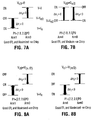
- FIGURES 7A and 7B illustrate a second embodiment of the present invention.
- no control voltage is supplied to the control pad and consequently the device behaves the same as that shown in FIGURE 4B.
- a control voltage of V( ⁇ /2) is supplied to the control pad on Arm 0. This effectively raises the voltage on Arm 0 so that it is biased between 0 and V( ⁇ /2), the same as Arm 1.
- This embodiment provides good extinction ratio and positive chirp which is not as good as provided by the embodiment of FIGURE 4A.
- the advantage of the embodiment of FIGURE 7B is that there is slightly less insertion loss than that for FIGURE 4A.
- FIGURES 8A and 8B A third embodiment is illustrated in FIGURES 8A and 8B.
- the difference in optical path length between Arm 1 and Arm 0 is only ⁇ /2 which, for an operating wavelength of 1.56 ⁇ m is 0.12 ⁇ m.
- the interferometer is provided with control voltage pads 30 and 34 on each arm as shown in Figure 3.
- the electric field is supplied to pad 30 via electrode 40 shown in broken line in Figure 3.
- a control electrode is required on just one arm (arm 0 in Figure 3) whereas a ⁇ /2 shifted device requires a control electrode on each arm.
- the control voltage is tuned to create the effective phase differential as previously discussed.
- Arm 0 is supplied with a control voltage of V ( ⁇ /2) while no voltage is supplied to Arm 1.
- Arm 1 is driven with a control voltage of ⁇ /2 and no voltage is supplied to Arm 0.
- the control voltage equivalent to a ⁇ /2 phase shift counteracts the phase differential.
- the control voltage equivalent to ⁇ /2 phase shift adds to the ⁇ /2 phase difference introduced by the length differential to equal a ⁇ phase shift.
Landscapes
- Physics & Mathematics (AREA)
- Nonlinear Science (AREA)
- Optics & Photonics (AREA)
- General Physics & Mathematics (AREA)
- Chemical & Material Sciences (AREA)
- Engineering & Computer Science (AREA)
- Nanotechnology (AREA)
- Life Sciences & Earth Sciences (AREA)
- Biophysics (AREA)
- Crystallography & Structural Chemistry (AREA)
- Optical Modulation, Optical Deflection, Nonlinear Optics, Optical Demodulation, Optical Logic Elements (AREA)
- Optical Communication System (AREA)
Claims (9)
- Multi-Quantum-Well-Mach-Zehnder-Phasenmodulator zum selektiven Erzeugen von positivem und negativem Frequenz-Chirp in einem optischen Signal mit einer bekannten Freiraumwellenlänge, wobei der Modulator Folgendes umfasst:einen Y-Übergang-Hohlleiterkoppler mit asymmetrischem Eingang mit einem Eingangshohlleiter (22) zum Empfangen des genannten optischen Signals und mit einem ersten und einem zweiten Eingangshohlleiterzweig;einen Y-Übergang-Hohlleiterkoppler (20) mit asymmetrischem Ausgang mit einem Ausgangshohlleiter zum Senden des genannten modulierten optischen Signals sowie mit einem ersten und einem zweiten Ausgangshohlleiterzweig;einen ersten interferometrischen Arm (24) zwischen ersten Hohlleiterzweigen der genannten Ein- und Ausgangs-Y-Übergangskoppler, der einen ersten Lichtweg definiert;einen zweiten interferometrischen Arm (26) zwischen zweiten Hohlleiterzweigen der genannten Ein- und Ausgangs-Y-Übergangskoppler, der einen zweiten Lichtweg definiert, wobei eine der genannten Weglängen um einen Betrag größer ist als die andere, der eine erste Phasendifferenz von π oder ein integrales ungeradzahliges Vielfaches von π bei der bekannten Wellenlänge und Null-Vorspannung erzeugt;Elektroden (28, 32) auf dem ersten und dem zweiten interferometrischen Arm zum Anlegen eines elektrischen Feldes zum Modulieren der wirksamen Phasendifferenz zwischen den genannten Armen; undeine Steuerelektrode (34) auf dem genannten ersten oder dem genannten zweiten Arm zum selektiven Anlegen eines elektrischen Steuerfeldes an den genannten einen Arm, um die Phasendifferenz zwischen den genannten Armen zu modulieren, so dass ohne elektrisches Feld an der genannten Steuerelektrode ein negativer Frequenz-Chirp erzeugt wird und mit einem elektrischen Steuerfeld an dem genannten einen Arm, das gleich der Spannung ist, die zum Erzeugen einer Phasendifferenz von π benötigt wird, oder ein ungeradzahliges Vielfache von π, ein positiver Frequenz-Chirp erzeugt wird.
- Multi-Quantum-Well-Mach-Zehnder-Phasenmodulator nach Anspruch 1, wobei der Y-Übergangskoppler 22 mit asymmetrischem Eingang das in den Modulator eintretende optische Signal so teilt, dass in dem längeren Lichtweg mehr Lichtenergie zu dem interferometrischen Arm geführt wird.
- Multi-Quantum-Well-Mach-Zehnder-Phasenmodulator nach Anspruch 2, wobei das Verhältnis der optischen Teilung im Bereich 1:1,8 bis 1:2,2 liegt, so gewählt, dass Elektroabsorption der Multi-Quantum-Well kompensiert wird.
- Multi-Quantum-Well-Mach-Zehnder-Phasenmodulator nach Anspruch 3, wobei die Steuerelektrode auf dem interferometrischen Arm ist, dem die geringere Lichtenergie zugeführt wird.
- Multi-Quantum-Well-Mach-Zehnder-Phasenmodulator zum selektiven Erzeugen von positivem und negativem Frequenz-Chirp in einem optischen Signal einer bekannten Freiraumwellenlänge, der Folgendes umfasst:einen Y-Übergang-Hohlleiterkoppler (22) mit asymmetrischem Eingang mit einem Eingangshohlleiter zum Empfangen des genannten optischen Signals sowie einer ersten und eine zweiten Eingangshohlleiterzweig-Steuerspannung;einen Y-Übergang-Hohlleiterkoppler (20) mit asymmetrischem Ausgang mit einem Ausgangshohlleiter zum Senden des genannten modulierten optischen Signals und einem ersten und einem zweiten Ausgangshohlleiterzweig;einen ersten interferometrischen Arm (24) zwischen ersten Hohlleiterzweigen der genannten Ein- und Ausgangs-Y-Übergangkoppler, der einen ersten Lichtweg definiert;einen zweiten interferometrischen Arm (26) zwischen zweiten Hohlleiterzweigen der genannten Ein- und Ausgangs-Y-Übergangskoppler, der einen zweiten Lichtweg definiert, wobei eine der genannten Weglängen um einen Betrag größer ist als die andere, der eine feste Phasendifferenz von π/2 an der bekannten Wellenlänge erzeugt;Elektroden an dem genannten ersten und dem genannten zweiten interferometrischen Arm zum Anlegen eines elektrischen Feldes zum Modulieren der wirksamen Phasendifferenz zwischen den genannten Armen; undeine Steuerelektrode an dem genannten ersten und dem genannten zweiten Arm zum selektiven Anlegen von elektrischen Steuerfeldern an jeden der genannten Arme, um die Phasendifferenz zwischen den genannten Armen zu modulieren, so dass ein elektrisches Feld zum Erzielen einer Phasendifferenz von π/2, das an die genannte Steuerelektrode an dem ersten Arm in Abwesenheit eines Feldes an der Elektrode am zweiten Arm angelegt wird, zu positivem Frequenz-Chirp führt, während ein gleiches elektrisches Feld, das an die Steuerelektrode am zweiten Arm angelegt wird, um eine Phasendifferenz von π/2 in Abwesenheit eines Feldes zur Elektrode am ersten Arm angelegt wird, zu negativem Frequenz-Chirp führt.
- Multi-Quantum-Well-Mach-Zehnder-Phasenmodulator nach Anspruch 5, wobei der Y-Übergangskoppler mit asymmetrischem Eingang das in den Modulator eintretende optische Signal so teilt, dass ein größerer Teil der Lichtenergie dem interferometrischen Arm in dem längeren Lichtweg zugeführt wird.
- Multi-Quantum-Well-Mach-Zehnder-Phasenmodulator nach Anspruch 6, wobei das Teilungsverhältnis von Lichtenergie im Bereich 1:2,2 bis 1:2,6 liegt, so gewählt, dass Elektroabsorption der Multi-Quantum-Well kompensiert wird.
- Verfahren zum selektiven Erzeugen von positivem und negativem Frequenz-Chirp in einem optischen Signal mit einer bekannten Freiraumwellenlänge, umfassend die folgenden Schritte:a) Koppeln des genannten optischen Signals mit einem Multi-Quantum-Well-Mach-Zehnder-Phasenmodulator mit einem Y-Übergangskoppler mit asymmetrischem Eingang und einem Y-Übergangskoppler mit asymmetrischen Ausgang mit einem ersten und einem zweiten interferometrischen Arm dazwischen, die einen ersten und einen zweiten Lichtweg definieren, von denen einer um einen Betrag länger ist als der andere, so dass eine feste Phasendifferenz von π oder ein integrales ungeradzahliges Vielfaches von π an der genannten bekannten Wellenlänge und Null-Vorspannung entsteht; eine erste und eine zweite Elektrode an jeweiligen Armen zum Empfangen eines modulierenden elektrischen Feldes, um deren wirksame Phasendifferenz einzustellen; und eine Steuerelektrode an einem der genannten interferometrischen Arme;b) Zuführen eines elektrischen Feldes zu jeder der genannten ersten und zweiten Elektroden in einer gleichen Gegentaktbeziehung, wobei die Amplitude des genannten elektrischen Feldes so gewählt wird, dass die genannte Phasendifferenz von π oder ein integrales ungeradzahliges Vielfaches von π entsteht; undc) selektives Zuführen eines elektrischen Feldes zu der genannten Steuerelektrode, so dass ein negativer Frequenz-Chirp ohne elektrisches Feld und ein positiver Frequenz-Chirp mit einem elektrischen Feld erzeugt wird, das gleich dem genannten elektrischen Feld ist, das zum Erzeugen der genannten Phasendifferenz von π oder einem integralen ungeradzahligen Vielfachen von π benötigt wird.
- Verfahren zum selektiven Erzeugen von positivem und negativem Frequenz-Chirp in einem optischen Signal mit einer bekannten Freiraumwellenlänge, umfassend die folgenden Schritte:a) Koppeln des genannten optischen Signals mit einem Multi-Quantum-Well-Mach-Zehnder-Phasenmodulator mit einem Y-Übergangskoppler mit asymmetrischem Eingang und einem Y-Übergangskoppler mit asymmetrischen Ausgang mit einem ersten und einem zweiten interferometrischen Arm dazwischen, die einen ersten und einen zweiten Lichtweg definieren, von denen einer um einen Betrag länger ist als der andere, so dass eine feste Phasendifferenz von π/2 an der genannten bekannten Wellenlänge und Null-Vorspannung entsteht; eine erste und eine zweite modulierende Elektrode an jeweiligen Armen zum Empfangen eines modulierenden elektrischen Feldes, um deren wirksame Phasendifferenz einzustellen; und eine erste und eine zweite Steuerelektrode an jeweiligen Armen;b) Zuführen eines elektrischen Feldes zu jeder der genannten ersten und zweiten modulierenden Elektroden in einer gleichen Gegentaktbeziehung, wobei die Amplitude des genannten elektrischen Feldes so gewählt wird, dass die genannte Phasendifferenz von π/2 entsteht; undc) selektives Zuführen eines elektrischen Feldes zu der einen oder der anderen der genannten Steuerelektroden, so dass ein Feld zu einer Steuerelektrode einen positiven Frequenz-Chirp und ein Feld zu der anderen Steuerelektrode einen negativen Frequenz-Chirp erzeugt.
Applications Claiming Priority (2)
| Application Number | Priority Date | Filing Date | Title |
|---|---|---|---|
| US08/745,168 US5778113A (en) | 1996-11-07 | 1996-11-07 | Configurable chirp Mach-Zehnder optical modulator |
| US745168 | 1996-11-07 |
Publications (3)
| Publication Number | Publication Date |
|---|---|
| EP0841587A2 EP0841587A2 (de) | 1998-05-13 |
| EP0841587A3 EP0841587A3 (de) | 1998-11-25 |
| EP0841587B1 true EP0841587B1 (de) | 2004-02-04 |
Family
ID=24995538
Family Applications (1)
| Application Number | Title | Priority Date | Filing Date |
|---|---|---|---|
| EP97308615A Expired - Lifetime EP0841587B1 (de) | 1996-11-07 | 1997-10-28 | Mach-Zehnder optischer Modulator mit einstellbarem Chirp und Verfahren zur Erzeugung einstellbaren Chirps |
Country Status (4)
| Country | Link |
|---|---|
| US (2) | US5778113A (de) |
| EP (1) | EP0841587B1 (de) |
| CA (1) | CA2220240C (de) |
| DE (1) | DE69727445T2 (de) |
Families Citing this family (48)
| Publication number | Priority date | Publication date | Assignee | Title |
|---|---|---|---|---|
| CA2218262C (en) * | 1996-10-17 | 2001-04-24 | Kenji Kawano | Ultra-high-speed semiconductor optical modulator with traveling-wave electrode |
| US5778113A (en) * | 1996-11-07 | 1998-07-07 | Northern Telecom Limited | Configurable chirp Mach-Zehnder optical modulator |
| JP2867995B2 (ja) * | 1997-05-28 | 1999-03-10 | 日本電気株式会社 | 半導体マハツェンダ変調器とその製造方法 |
| AU9187198A (en) * | 1997-10-02 | 1999-04-27 | Sumitomo Electric Industries, Ltd. | Dispersion shift optical fiber |
| GB2331373B (en) * | 1997-11-12 | 2000-02-23 | Bookham Technology Ltd | Optical system and method for changing the lengths of optical paths and the phases of light beams |
| US6233070B1 (en) * | 1998-05-19 | 2001-05-15 | Bookham Technology Plc | Optical system and method for changing the lengths of optical paths and the phases of light beams |
| JP3337980B2 (ja) * | 1998-06-29 | 2002-10-28 | 沖電気工業株式会社 | 光送信器及び光伝送システム |
| JP4094761B2 (ja) * | 1999-03-01 | 2008-06-04 | 富士通株式会社 | 光変調装置、復調装置、その方法、光送信機及び光受信機 |
| US6393166B1 (en) * | 2000-03-27 | 2002-05-21 | Codeon Corporation | Variable chirp modulator having three arm interferometer |
| GB2375614B (en) * | 2000-04-06 | 2003-07-16 | Bookham Technology Plc | Optical modulator with pre-determined frequency chirp |
| GB0008536D0 (en) * | 2000-04-06 | 2000-05-24 | Marconi Caswell Ltd | Optical modulator with selectable frequency chirp |
| JP2002182172A (ja) * | 2000-10-03 | 2002-06-26 | Fujitsu Ltd | 光変調器 |
| GB2370369B (en) * | 2000-12-21 | 2004-07-14 | Nortel Networks Ltd | Optical Modulators |
| EP1233562B1 (de) * | 2001-02-14 | 2004-11-03 | Alcatel | Modulierungsschema und Übertragungssystem für NRZ-Signale mit links- und rechtsseitiger Filterung |
| US6552837B2 (en) | 2001-02-15 | 2003-04-22 | Modetek, Inc | Optical modulator with integrated driver |
| US6501867B2 (en) | 2001-04-17 | 2002-12-31 | Lucent Technologies Inc. | Chirp compensated Mach-Zehnder electro-optic modulator |
| US6741761B2 (en) * | 2001-06-28 | 2004-05-25 | Sycamore Networks, Inc. | Method for achieving improved transmission performance over fiber using a Mach-Zehnder modulator |
| US6980746B2 (en) * | 2001-09-17 | 2005-12-27 | Dorsal Networks, Inc. | Electronic RZ/CSRZ signal generation for optical communication systems |
| US6714695B2 (en) | 2001-09-17 | 2004-03-30 | Dorsal Networks, Inc. | Optical transmission system employing auto-synchronized chirped return-to-zero transmitter |
| US6882758B2 (en) * | 2002-07-09 | 2005-04-19 | Bookham Technology Plc | Current tuned Mach-Zehnder optical attenuator |
| US6650458B1 (en) * | 2002-09-26 | 2003-11-18 | Bookham Technology Plc | Electro-optic modulator with continuously adjustable chirp |
| US6795594B2 (en) * | 2002-10-03 | 2004-09-21 | Nortel Networks Limited | Duobinary modulation scheme for a Mach-Zehnder optical modulator |
| US7633988B2 (en) * | 2003-07-31 | 2009-12-15 | Jds Uniphase Corporation | Tunable laser source with monolithically integrated interferometric optical modulator |
| US8149492B2 (en) * | 2004-03-31 | 2012-04-03 | Google Inc. | Optical modulator |
| EP1596246B1 (de) * | 2004-05-13 | 2016-12-14 | Fujitsu Limited | Optischer Halbleiter-Modulator und optisches Modulationsverfahren |
| JP4272585B2 (ja) * | 2004-05-13 | 2009-06-03 | 富士通株式会社 | 光変調装置、光送信装置及び光変調方法 |
| JP4235154B2 (ja) * | 2004-08-27 | 2009-03-11 | 富士通株式会社 | 半導体マッハツェンダ型光変調器及びその製造方法 |
| JP2006100909A (ja) * | 2004-09-28 | 2006-04-13 | Nec Corp | 波長分割多重光伝送システム、光送信装置、中継ノード及び波長分割多重光伝送方法 |
| USRE44647E1 (en) | 2005-03-15 | 2013-12-17 | Emcore Corporation | Directly modulated laser optical transmission system with phase modulation |
| US7848661B2 (en) * | 2005-03-15 | 2010-12-07 | Emcore Corporation | Directly modulated laser optical transmission system with phase modulation |
| JP4696264B2 (ja) * | 2005-08-24 | 2011-06-08 | 独立行政法人情報通信研究機構 | 強度バランス機能を有する光fsk/ssb変調器 |
| JP4872319B2 (ja) * | 2005-11-18 | 2012-02-08 | 日本電気株式会社 | 光信号送受信システム、光波長多重伝送システム、光送受信装置、および光波長多重伝送方法 |
| US7499603B1 (en) | 2006-01-19 | 2009-03-03 | Lockheed Martin Corporation | Range extended electrooptic modulator |
| US7792432B2 (en) * | 2006-03-02 | 2010-09-07 | Emcore Corporation | Externally modulated laser optical transmission system with feed forward noise cancellation |
| US7881621B2 (en) | 2006-03-02 | 2011-02-01 | Emcore Corporation | Optical transmission system with directly modulated laser and feed forward noise cancellation |
| JP2007248850A (ja) * | 2006-03-16 | 2007-09-27 | Oki Electric Ind Co Ltd | マッハツェンダ型半導体素子及びその制御方法 |
| US7483597B2 (en) * | 2006-10-19 | 2009-01-27 | Lightwire, Inc. | Optical modulator utilizing multi-level signaling |
| US8064778B2 (en) * | 2007-03-23 | 2011-11-22 | Emcore Corporation | Method and apparatus for controlling tunable transmitter chirp |
| JP5299859B2 (ja) * | 2008-01-28 | 2013-09-25 | 独立行政法人情報通信研究機構 | 超平坦光周波数コム信号発生器 |
| JP5181999B2 (ja) * | 2008-10-10 | 2013-04-10 | ソニー株式会社 | 固体撮像素子、光学装置、信号処理装置及び信号処理システム |
| US8442361B1 (en) * | 2008-11-19 | 2013-05-14 | Lockheed Martin Corporation | Apparatus and method of linearization in an optical modulator |
| JP5267105B2 (ja) * | 2008-12-22 | 2013-08-21 | 富士通株式会社 | 光モジュール及びその製造方法、光送信器 |
| US8452179B2 (en) * | 2010-02-26 | 2013-05-28 | Cisco Technology, Inc. | Remotely settable chromatic dispersion robustness for dense wave division multiplexing interfaces |
| WO2015154813A1 (en) * | 2014-04-10 | 2015-10-15 | Fraunhofer-Gesellschaft zur Förderung der angewandten Forschung e.V. | Mach-zehnder modulator and method for operating a mach-zehnder modulator |
| JP6306939B2 (ja) * | 2014-05-21 | 2018-04-04 | 日本電信電話株式会社 | マッハツェンダ型光変調器の制御方法 |
| US10120210B2 (en) * | 2016-06-03 | 2018-11-06 | International Business Machines Corporation | Feed-forward optical equalization using an electro-optic modulator with a multi-segment electrode and distributed drivers |
| CN113014323B (zh) | 2019-12-20 | 2024-02-09 | 光联通讯技术有限公司美国分部 | 光传送装置及光通信系统 |
| CN117991445A (zh) * | 2022-11-07 | 2024-05-07 | 华为技术有限公司 | 光功率分配 |
Family Cites Families (5)
| Publication number | Priority date | Publication date | Assignee | Title |
|---|---|---|---|---|
| US5365338A (en) * | 1991-05-28 | 1994-11-15 | The United States Of America As Represented By The Secretary Of The Navy | Wavelength sensor for fiber optic gyroscope |
| US5550513A (en) * | 1995-06-22 | 1996-08-27 | Northern Telecom Limited | High frequency, differential limiting distributed amplifier |
| GB2302738B (en) * | 1995-06-28 | 1999-03-03 | Northern Telecom Ltd | Semiconductor modulator with a shift |
| US5778113A (en) * | 1996-11-07 | 1998-07-07 | Northern Telecom Limited | Configurable chirp Mach-Zehnder optical modulator |
| JPH10239539A (ja) * | 1997-02-24 | 1998-09-11 | Fujitsu Ltd | 光分岐装置及び光分岐出力制御方法 |
-
1996
- 1996-11-07 US US08/745,168 patent/US5778113A/en not_active Expired - Lifetime
-
1997
- 1997-10-28 DE DE69727445T patent/DE69727445T2/de not_active Expired - Lifetime
- 1997-10-28 EP EP97308615A patent/EP0841587B1/de not_active Expired - Lifetime
- 1997-11-05 CA CA002220240A patent/CA2220240C/en not_active Expired - Fee Related
-
1998
- 1998-04-09 US US09/057,602 patent/US5991471A/en not_active Expired - Lifetime
Also Published As
| Publication number | Publication date |
|---|---|
| US5778113A (en) | 1998-07-07 |
| CA2220240A1 (en) | 1998-05-07 |
| EP0841587A2 (de) | 1998-05-13 |
| DE69727445D1 (de) | 2004-03-11 |
| CA2220240C (en) | 2001-08-28 |
| EP0841587A3 (de) | 1998-11-25 |
| US5991471A (en) | 1999-11-23 |
| DE69727445T2 (de) | 2004-12-16 |
Similar Documents
| Publication | Publication Date | Title |
|---|---|---|
| EP0841587B1 (de) | Mach-Zehnder optischer Modulator mit einstellbarem Chirp und Verfahren zur Erzeugung einstellbaren Chirps | |
| US5524076A (en) | Chirp control of a Mach-Zehnder optical modulator using non-equal power splitting | |
| US8149492B2 (en) | Optical modulator | |
| EP0950167B1 (de) | Variabler optischer Chirp Modulator mit einer einzigen Modulationsquelle | |
| US5303079A (en) | Tunable chirp, lightwave modulator for dispersion compensation | |
| US6778309B2 (en) | Electroabsorption modulator with tunable chirp | |
| US6583917B2 (en) | Optical intensity modulation device and method | |
| CA2176099C (en) | Semiconductor modulator with a shift | |
| EP2545408B1 (de) | Optische modulatoren mit steuerbarer frequenzmodulation | |
| US7068948B2 (en) | Generation of optical signals with return-to-zero format | |
| US7911675B2 (en) | Optical modulation device and optical semiconductor device | |
| US20130094797A1 (en) | Optical Transmitter With Tunable Chirp | |
| Lawetz et al. | Modulation characteristics of semiconductor Mach-Zehnder optical modulators | |
| EP1424591A1 (de) | Elektrooptischer Modulator und Verfahren zur Modulierung optischer Signale | |
| US20090220185A1 (en) | Light modulating device | |
| EP1217425B1 (de) | Optischer Intensitätsmodulator und zugehöriges Verfahren | |
| US6947617B2 (en) | Polarized wave scrambler and optical signal transmission apparatus | |
| Doerr | InP-Based Photonic Devices; Focusing on devices for fiber-optic communications that monolithically integrate two or more functions | |
| JP2000241775A (ja) | 光変調器と光通信用光源及び光通信用モジュール | |
| Ho | Advanced Topics in Lightwave Communications Generation of Optical Signals | |
| Wooten et al. | An Analysis of Lithium Niobate Modulators for Optical Fiber Networks | |
| Walker et al. | Integrated high-functionality GaAs modulators for 10 & 40 Gb/s transmission | |
| Hu et al. | 10Gbps zero-chirp compact transmitter with InP MQW Mach-Zehnder modulator | |
| JPH06118460A (ja) | 光位相変調回路 | |
| CA2272376A1 (en) | Variable chirp optical modulator using single modulation source |
Legal Events
| Date | Code | Title | Description |
|---|---|---|---|
| PUAI | Public reference made under article 153(3) epc to a published international application that has entered the european phase |
Free format text: ORIGINAL CODE: 0009012 |
|
| AK | Designated contracting states |
Kind code of ref document: A2 Designated state(s): DE FR GB IT |
|
| PUAL | Search report despatched |
Free format text: ORIGINAL CODE: 0009013 |
|
| AK | Designated contracting states |
Kind code of ref document: A3 Designated state(s): AT BE CH DE DK ES FI FR GB GR IE IT LI LU MC NL PT SE |
|
| RAP3 | Party data changed (applicant data changed or rights of an application transferred) |
Owner name: NORTEL NETWORKS CORPORATION |
|
| 17P | Request for examination filed |
Effective date: 19990525 |
|
| AKX | Designation fees paid |
Free format text: DE FR GB IT |
|
| RAP1 | Party data changed (applicant data changed or rights of an application transferred) |
Owner name: NORTEL NETWORKS LIMITED |
|
| 17Q | First examination report despatched |
Effective date: 20010116 |
|
| GRAP | Despatch of communication of intention to grant a patent |
Free format text: ORIGINAL CODE: EPIDOSNIGR1 |
|
| RAP1 | Party data changed (applicant data changed or rights of an application transferred) |
Owner name: BOOKHAM TECHNOLOGY PLC |
|
| RTI1 | Title (correction) |
Free format text: CONFIGURABLE CHIRP MACH-ZEHNDER OPTICAL MODULATOR AND METHOD OF GENERATING SELECTABLE FREQUENCY CHIRP |
|
| RTI1 | Title (correction) |
Free format text: CONFIGURABLE CHIRP MACH-ZEHNDER OPTICAL MODULATOR AND METHOD OF GENERATING SELECTABLE FREQUENCY CHIRP |
|
| GRAS | Grant fee paid |
Free format text: ORIGINAL CODE: EPIDOSNIGR3 |
|
| GRAA | (expected) grant |
Free format text: ORIGINAL CODE: 0009210 |
|
| AK | Designated contracting states |
Kind code of ref document: B1 Designated state(s): DE FR GB IT |
|
| PG25 | Lapsed in a contracting state [announced via postgrant information from national office to epo] |
Ref country code: IT Free format text: LAPSE BECAUSE OF FAILURE TO SUBMIT A TRANSLATION OF THE DESCRIPTION OR TO PAY THE FEE WITHIN THE PRE;WARNING: LAPSES OF ITALIAN PATENTS WITH EFFECTIVE DATE BEFORE 2007 MAY HAVE OCCURRED AT ANY TIME BEFORE 2007. THE CORRECT EFFECTIVE DATE MAY BE DIFFERENT FROM THE ONE RECORDED.SCRIBED TIME-LIMIT Effective date: 20040204 |
|
| REG | Reference to a national code |
Ref country code: GB Ref legal event code: FG4D |
|
| REF | Corresponds to: |
Ref document number: 69727445 Country of ref document: DE Date of ref document: 20040311 Kind code of ref document: P |
|
| 111Z | Information provided on other rights and legal means of execution |
Free format text: DEFRGBIT Effective date: 20031030 |
|
| ET | Fr: translation filed | ||
| PLBE | No opposition filed within time limit |
Free format text: ORIGINAL CODE: 0009261 |
|
| STAA | Information on the status of an ep patent application or granted ep patent |
Free format text: STATUS: NO OPPOSITION FILED WITHIN TIME LIMIT |
|
| 26N | No opposition filed |
Effective date: 20041105 |
|
| REG | Reference to a national code |
Ref country code: GB Ref legal event code: 732E |
|
| PGFP | Annual fee paid to national office [announced via postgrant information from national office to epo] |
Ref country code: DE Payment date: 20131023 Year of fee payment: 17 Ref country code: FR Payment date: 20131009 Year of fee payment: 17 Ref country code: GB Payment date: 20131023 Year of fee payment: 17 |
|
| REG | Reference to a national code |
Ref country code: GB Ref legal event code: 732E Free format text: REGISTERED BETWEEN 20140612 AND 20140618 |
|
| REG | Reference to a national code |
Ref country code: FR Ref legal event code: CD Owner name: OCLARO TECHNOLOGY LIMITED Effective date: 20140930 |
|
| REG | Reference to a national code |
Ref country code: DE Ref legal event code: R082 Ref document number: 69727445 Country of ref document: DE Representative=s name: PATENTANWAELTE WALLACH, KOCH & PARTNER, DE |
|
| REG | Reference to a national code |
Ref country code: DE Ref legal event code: R119 Ref document number: 69727445 Country of ref document: DE |
|
| REG | Reference to a national code |
Ref country code: DE Ref legal event code: R082 Ref document number: 69727445 Country of ref document: DE Representative=s name: PATENTANWAELTE WALLACH, KOCH, DR. HAIBACH, FEL, DE Effective date: 20150422 Ref country code: DE Ref legal event code: R082 Ref document number: 69727445 Country of ref document: DE Representative=s name: PATENTANWAELTE WALLACH, KOCH & PARTNER, DE Effective date: 20150422 Ref country code: DE Ref legal event code: R081 Ref document number: 69727445 Country of ref document: DE Owner name: OCLARO TECHNOLOGY LIMITED, TOWCESTER, GB Free format text: FORMER OWNER: BOOKHAM TECHNOLOGY PLC, ABINGDON, OXFORDSHIRE, GB Effective date: 20150422 |
|
| GBPC | Gb: european patent ceased through non-payment of renewal fee |
Effective date: 20141028 |
|
| PG25 | Lapsed in a contracting state [announced via postgrant information from national office to epo] |
Ref country code: DE Free format text: LAPSE BECAUSE OF NON-PAYMENT OF DUE FEES Effective date: 20150501 Ref country code: GB Free format text: LAPSE BECAUSE OF NON-PAYMENT OF DUE FEES Effective date: 20141028 |
|
| REG | Reference to a national code |
Ref country code: FR Ref legal event code: ST Effective date: 20150630 |
|
| PG25 | Lapsed in a contracting state [announced via postgrant information from national office to epo] |
Ref country code: FR Free format text: LAPSE BECAUSE OF NON-PAYMENT OF DUE FEES Effective date: 20141031 |