US6980746B2 - Electronic RZ/CSRZ signal generation for optical communication systems - Google Patents
Electronic RZ/CSRZ signal generation for optical communication systems Download PDFInfo
- Publication number
- US6980746B2 US6980746B2 US09/953,567 US95356701A US6980746B2 US 6980746 B2 US6980746 B2 US 6980746B2 US 95356701 A US95356701 A US 95356701A US 6980746 B2 US6980746 B2 US 6980746B2
- Authority
- US
- United States
- Prior art keywords
- signal
- clock signal
- data signal
- switch
- csrz
- Prior art date
- Legal status (The legal status is an assumption and is not a legal conclusion. Google has not performed a legal analysis and makes no representation as to the accuracy of the status listed.)
- Expired - Fee Related, expires
Links
Images


Classifications
-
- H—ELECTRICITY
- H04—ELECTRIC COMMUNICATION TECHNIQUE
- H04B—TRANSMISSION
- H04B10/00—Transmission systems employing electromagnetic waves other than radio-waves, e.g. infrared, visible or ultraviolet light, or employing corpuscular radiation, e.g. quantum communication
- H04B10/50—Transmitters
- H04B10/501—Structural aspects
- H04B10/503—Laser transmitters
- H04B10/505—Laser transmitters using external modulation
-
- H—ELECTRICITY
- H04—ELECTRIC COMMUNICATION TECHNIQUE
- H04B—TRANSMISSION
- H04B10/00—Transmission systems employing electromagnetic waves other than radio-waves, e.g. infrared, visible or ultraviolet light, or employing corpuscular radiation, e.g. quantum communication
- H04B10/50—Transmitters
- H04B10/508—Pulse generation, e.g. generation of solitons
-
- H—ELECTRICITY
- H04—ELECTRIC COMMUNICATION TECHNIQUE
- H04B—TRANSMISSION
- H04B10/00—Transmission systems employing electromagnetic waves other than radio-waves, e.g. infrared, visible or ultraviolet light, or employing corpuscular radiation, e.g. quantum communication
- H04B10/50—Transmitters
- H04B10/516—Details of coding or modulation
- H04B10/5162—Return-to-zero modulation schemes
-
- H—ELECTRICITY
- H04—ELECTRIC COMMUNICATION TECHNIQUE
- H04B—TRANSMISSION
- H04B10/00—Transmission systems employing electromagnetic waves other than radio-waves, e.g. infrared, visible or ultraviolet light, or employing corpuscular radiation, e.g. quantum communication
- H04B10/50—Transmitters
- H04B10/516—Details of coding or modulation
- H04B10/5165—Carrier suppressed; Single sideband; Double sideband or vestigial
-
- H—ELECTRICITY
- H04—ELECTRIC COMMUNICATION TECHNIQUE
- H04B—TRANSMISSION
- H04B10/00—Transmission systems employing electromagnetic waves other than radio-waves, e.g. infrared, visible or ultraviolet light, or employing corpuscular radiation, e.g. quantum communication
- H04B10/50—Transmitters
- H04B10/516—Details of coding or modulation
- H04B10/54—Intensity modulation
- H04B10/541—Digital intensity or amplitude modulation
Definitions
- the field of the present invention is optical communications. Specifically, the present invention is directed to a device and method for generating both RZ and CSRZ signals using only one optical modulator.
- RZ return to zero
- CSRZ carrier suppressed return to zero
- both RZ and CSRZ signals have their benefits in optical communications.
- CSRZ shaped signals may be preferable for use in DWDM (dense wave division multiplexing) applications.
- CSRZ signals have lesser bandwidth so, in narrow channel spacing configurations like DWDM, the use of CSRZ can be better than regular RZ in reducing linear and even non-linear crosstalk.
- the present invention provides a solution to the foregoing problem. Specifically, the invention provides an inexpensive way to generate both RZ and CSRZ shaped signals using only a single optical modulator.
- the present invention is directed to an optical communications system and method for generating both return-to-zero (RZ) and carrier suppressed return-to-zero (CSRZ) signals, where the system includes: a switch for receiving a data signal and a clock signal as inputs, and outputting a voltage signal; a unit for controllably adjusting the phase of said clock signal before input to the switch; an optical modulator for receiving a continuous wave light (CW) signal and the voltage signal as inputs, and outputting one of an RZ and a CSRZ signal.
- CW continuous wave light
- the optical modulator is biased at a transmission minimum level signal.
- the optical modulator is biased at a transmission maximum level and the clock signal is phase shifted.
- the present invention is also directed to an optical communication transceiver including a plurality of optical modulator circuits generating both RZ and CSRZ signals.
- Each modulator circuit includes: a switch for receiving a data signal and a clock signal as inputs, and outputting a voltage signal; a unit for controllably adjusting the phase of at least one of the data signal and the clock signal before input to the switch; an optical modulator for receiving a continuous wave light (CW) signal and the voltage signal as inputs, and outputting one of an RZ and a CSRZ signal.
- CW continuous wave light
- the optical modulator is biased at a transmission minimum level.
- the transceiver also includes a wavelength division multiplexer for combining the generated signals from the plurality of optical modulator circuits for transmission.
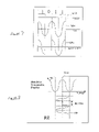
- FIG. 1 illustrates a signal shaping system of the prior art in which two optical modulators are used
- FIGS. 2 and 3 show modular transmission functions and clock signals used to generate RZ shaped signals
- FIG. 4 shows the modulator transmission function and clock signal used to generate a CSRZ shaped signal
- FIG. 5 illustrates a system according to the present invention for generating an RZ shaped signal using only a single optical modulator
- FIGS. 6A–6C illustrate configurations of a system according to the present invention for generating either an RZ or a CSRZ shaped signal using only a single optical modulator
- FIG. 7 is a timing diagram illustrating various signals used in the system of the present invention for generating an RZ shaped signal
- FIG. 8 illustrates the modulator transmission function and the modulating signal used to generate an RZ shaped signal in the present invention
- FIG. 9 is a timing diagram illustrating the various signals used to generate a CSRZ shaped signal in the present invention.
- FIG. 10 illustrates the modulator transmission function and the modulating signal used to generate a CSRZ signal in the present invention.
- the present invention is now described in detail with reference to the above-mentioned figures.
- the present invention can be summarized as a method and system for use in optical communications for generating both RZ and CSRZ signals.
- FIG. 1 illustrates a system configuration used in optical communications for shaping RZ and CSRZ signals.
- laser 110 provides a continuous wave light (CW) signal 120 to an optical modulator 30 .
- the data signal 140 to be transmitted is input to the optical modulator 130 to generate the output signal 150 which is a non-return to zero (NRZ) signal.
- This NRZ signal is an optical signal representing the data stream and contains a stream of square shaped light pulses where a “light on” condition represents a data 1 and a “light off” (or effectively off) condition represents a data 0 .
- This NRZ signal 150 is then shaped by a second modulator 160 .
- the modulating signal input to the optical modulator 160 is the clock signal 170 . In this way the NRZ signal 150 is shaped into the sinusoidal pulses of an RZ or a CSRZ signal 180 .
- FIG. 2 illustrates the modulator transmission function of the second optical modulator 160 , as well as the clock signal 170 which is input to that modulator.
- the modulator transmission function is shown as graph 210 .
- the clock or voltage signal input to the optical modulator is shown as graph 170 .
- the center level of this voltage signal 170 that is, the bias of the modulator is shown as dotted line 220 .
- the optical modulator is biased at a transmission maximum level; see, for example, line 220 intersecting graph 210 at the maximum level of transmission of the optical modulator.
- the clock signal 170 is set to have a frequency of one-half the frequency of the data signal.
- RZ signal is meant to refer to regular RZ or non-carrier suppressed RZ as it is sometimes called.
- FIG. 3 illustrates the modulator transmission function of optical modulator 160 along with the clock signal 170 .
- This configuration illustrates another method for generating RZ shaped signals.
- the modulator function is shown as 310 and the center level of the clock signal is shown as dotted line 320 .
- the modulator is biased at the midpoint between transmission maximum and transmission minimum level, as is shown by the intersection of dotted line 320 with the graph 310 .
- the frequency of the clock signal is the same as that of the data signal. With this combination an RZ shaped signal can be generated.
- FIG. 4 illustrates such a configuration and shows the modular transmission function 410 of the optical modulator 160 along with the clock signal 170 .
- the center level of this clock signal is shown with dotted line 420 .
- the optical modulator is biased at a transmission minimum level as shown by the intersection of line 420 with graph 410 .
- the clock signal 170 has a frequency one half that of the data signal. With this configuration a carrier suppressed RZ shaped signal can be generated.
- FIGS. 1–4 are directed to optical generation of RZ or CSRZ signals in the prior art.
- optical modulators are very expensive and it would be preferable to have a system that would provide signal shaping at a lower cost.
- FIG. 5 One such system is shown in FIG. 5 .
- laser 510 provides a CW signal 520 to an optical modulator 530 .
- the modulating signal 570 provided to the optical modulator 530 is the output of a logic AND gate 540 .
- the data signal 550 and the clock signal 560 are the inputs to the AND gate 540 . With this combination of the data and clock signals being input to the modulator 530 , an RZ shaped signal 580 is generated at the output.
- This system has the benefit of needing only one optical modulator and provides for RZ shaping “electronically” so to speak, through the use of a logic AND gate 540 .
- this system suffers from the drawback that the user has no control to generate a CSRZ shaped signal. That is, only a regular RZ signal can be generated.
- the device of the present invention address this problem.
- the AND gate 540 has been replaced by a switch 640 .
- laser 610 provides a CW signal 620 to an optical modulator 630 .
- This modulator is modulated by a signal 690 which is the output of switch 640 .
- One input to switch 640 is the data signal 650 .
- This data signal controls the operation of the switch. That is, the switch is opened or closed based on the data signal. When the data signal is a logic level 1 the switch is open, and when the signal is a logic level 0 the switch is closed.
- switch 640 is an analog electronic switch that can output both positive and negative voltages.
- One limitation of this switch is its speed. Applicant envisions that, based on the availability of higher speed switches, the invention described herein could be used for higher speed data transmission.
- FIG. 6A which illustrates a first embodiment of the present invention
- a delay unit 670 placed between the source of the clock signal 660 and the switch 640 .
- This delay unit allows for the phase shifting of the clock signal 660 and is preferably a standard electronic delay line that is adjustable.
- FIG. 6B which illustrates a second embodiment of the present invention
- the same configuration as that of FIG. 6A is found except for the location of delay unit 670 .
- delay unit 670 is placed between the source of data signal 650 and the switch 640 .
- the role of the delay unit 670 in this scenario is to phase shift the data signal 650 .
- FIG. 6A which illustrates a first embodiment of the present invention
- the delay unit 670 is positioned such that it receives both the data signal 650 and the clock signal 660 , which are then output to the switch 640 . Its role in this scenario is to adjust the relative phase between the data signal and the clock signal by adjusting one or both of these signals.
- FIGS. 7 and 8 illustrate the timing diagrams, transmission functions and clock signals used to generate an RZ shaped signal using the method and device of the present invention.
- a small segment of the data signal 650 is shown.
- Four bits of the signal are shown as 1-0-1-1.
- the sinusoidal voltage signal under the data signal 650 is the clock signal 660 .
- the frequency of this clock signal is one half that of the data signal. Initially, these two signals are in-phase. However, as shown, clock signal 660 is out of phase with respect to the data signal by one-half bit or alternatively, one-quarter cycle of the clock signal.
- This phase shift is accomplished using a delay unit 670 and can be performed on solely the clock signal as shown in FIG. 6A , solely the data signal as shown in FIG. 6B , or potentially on both signals such that the relative phase difference is one half bit, as can be accomplished through the configuration shown in FIG. 6C .
- the data signal and the clock signal are input to the switch 640 with the operation of the switch being controlled by the data signal.
- the switch is open and the clock signal is allowed to pass through to the switch output 690 .
- the switch is closed and the clock signal is prevented from passing through.
- the switch output 690 then is at a zero voltage level.
- This switch output signal is then input to the optical modulator 630 as the modulating signal for shaping the CW signal 620 .
- FIG. 8 illustrates the modulator transmission function 810 along with the modulating signal that is the switch output signal 690 .
- the center level of this voltage signal is shown as dotted line 820 .
- the optical modulator 630 is biased at a transmission maximum level. This is indicated by the line 820 intersecting the graph 810 at a transmission maximum level.
- RZ signal shaping can be accomplished.
- delay unit 670 is controlled by the user and is set to create a delay or phase shift when RZ signal shaping is desired.
- the optical modulator 630 is biased at a transmission maximum level.
- FIGS. 9 and 10 illustrate how a CSRZ shaped signal can be generated using the same device as shown in FIGS. 6A–6C of the present invention.
- the same data signal 650 is shown, as well as the same clock signal 660 , however, in this scenario there is no phase shift between the clock signal and the data signal.
- the frequency of the clock signal is one half that of the data signal.
- the data signal controls the switch 640 as discussed above, resulting in the passing of the clock signal 660 to the switch output 690 during the period when the data signal is a logic level high or 1 and prevents the passing of the clock signal when the data signal is at a logic level low or 0. This is shown by the switch output diagram 690 in FIG. 9 .
- FIG. 10 illustrates the modular transmission function 1010 of the optical modulator 630 as well as the switch output signal 690 .
- the center level of this switch output voltage signal is shown with dashed line 1020 .
- the optical modulator 630 is biased at a transmission minimum level. This is shown by the intersection of line 1020 with graph 1010 at a transmission minimum level.
- CSRZ shaping can be accomplished. Specifically, the data signal and clock signal are in phase since the delay unit 670 is either logically removed or set to have no phase shift impact on the signals. Also, the optical modulator 630 is set to bias at a transmission minimum level. With this combination, CSRZ shaping is accomplished.
- both RZ and CSRZ shaping can be accomplished using the same device as shown in FIGS. 6A–6C by simply changing the bias level of the optical modulator 630 and controlling the phase difference between the data and clock signal.
- optical modulator circuits that are capable of generating both return to zero and carrier suppressed return to zero signals can be used together in order to generate a plurality of such signals for combination using wavelength division multiplexing and subsequent transmission.
Landscapes
- Physics & Mathematics (AREA)
- Electromagnetism (AREA)
- Engineering & Computer Science (AREA)
- Computer Networks & Wireless Communication (AREA)
- Signal Processing (AREA)
- Optics & Photonics (AREA)
- Optical Communication System (AREA)
Abstract
Description
Claims (38)
Priority Applications (1)
| Application Number | Priority Date | Filing Date | Title |
|---|---|---|---|
| US09/953,567 US6980746B2 (en) | 2001-09-17 | 2001-09-17 | Electronic RZ/CSRZ signal generation for optical communication systems |
Applications Claiming Priority (1)
| Application Number | Priority Date | Filing Date | Title |
|---|---|---|---|
| US09/953,567 US6980746B2 (en) | 2001-09-17 | 2001-09-17 | Electronic RZ/CSRZ signal generation for optical communication systems |
Publications (2)
| Publication Number | Publication Date |
|---|---|
| US20030053179A1 US20030053179A1 (en) | 2003-03-20 |
| US6980746B2 true US6980746B2 (en) | 2005-12-27 |
Family
ID=25494198
Family Applications (1)
| Application Number | Title | Priority Date | Filing Date |
|---|---|---|---|
| US09/953,567 Expired - Fee Related US6980746B2 (en) | 2001-09-17 | 2001-09-17 | Electronic RZ/CSRZ signal generation for optical communication systems |
Country Status (1)
| Country | Link |
|---|---|
| US (1) | US6980746B2 (en) |
Cited By (4)
| Publication number | Priority date | Publication date | Assignee | Title |
|---|---|---|---|---|
| US20030175037A1 (en) * | 2002-03-15 | 2003-09-18 | Mintera Corporation | Control of an optical modulator for desired biasing of data and pulse modulators |
| US20030185575A1 (en) * | 2002-03-26 | 2003-10-02 | Fujitsu Limited | Drive control apparatus and drive control method for optical modulator |
| US20040184818A1 (en) * | 2003-03-19 | 2004-09-23 | Lee Dong Soo | Apparatus for generating optical carrier suppressed return-to-zero |
| US20100309961A1 (en) * | 2009-06-08 | 2010-12-09 | Elrabaa Muhammad E S | Two-phase return-to-zero asynchronous transceiver |
Families Citing this family (6)
| Publication number | Priority date | Publication date | Assignee | Title |
|---|---|---|---|---|
| US20030067655A1 (en) * | 2001-10-05 | 2003-04-10 | Bo Pedersen | Methods and systems for integrated IP routers and long haul/ultra long haul optical communication transceivers |
| KR100493095B1 (en) * | 2002-10-16 | 2005-06-02 | 삼성전자주식회사 | Optical transmitting system |
| KR100600996B1 (en) * | 2003-10-24 | 2006-07-19 | 한국전자통신연구원 | Optical transmitter for generating duobinary csrz signal and csrz-dpsk signal with enlarged dispersion tolerance for optical communication system |
| EP1686706B1 (en) * | 2005-02-01 | 2007-05-30 | Alcatel Lucent | Method for modulating an optical signal and optical transmitter |
| KR100687753B1 (en) * | 2005-10-19 | 2007-02-27 | 한국전자통신연구원 | Apparatus and method to generate carrier suppressed-return to zero optical signal |
| CN103297016B (en) * | 2012-03-01 | 2020-06-19 | 朗美通技术英国有限公司 | Optical transmitter and optical communication method |
Citations (8)
| Publication number | Priority date | Publication date | Assignee | Title |
|---|---|---|---|---|
| US5521738A (en) * | 1994-06-30 | 1996-05-28 | At&T Corp. | Data encoded optical pulse generator |
| US5828477A (en) | 1995-11-16 | 1998-10-27 | Harmonic Lightwaves, Inc. | Multi-tone phase modulation for light wave communication system |
| US5991471A (en) | 1996-11-07 | 1999-11-23 | Nortel Networks Corporation | Configurable chirp mach-zehnder optical modulator |
| EP0964538A2 (en) | 1998-06-09 | 1999-12-15 | NEC Corporation | Optical transmitter and optical transmission system using polarisation modulation |
| US6014479A (en) | 1996-10-10 | 2000-01-11 | Tyco Submarine Systems Ltd. | High channel density wavelength division multiplex (WDM) optical transmission system and method with negligible four-wave mixing (FWM) penalty |
| US6072615A (en) | 1997-06-13 | 2000-06-06 | Lucent Technologies Inc. | Phase modulator-based generation of high-quality high bit rate return-to-zero optical data streams |
| EP1041754A1 (en) | 1999-04-01 | 2000-10-04 | PIRELLI CAVI E SISTEMI S.p.A. | Method for the reduction of noise in a long-distance optical telecommunications system |
| US6718142B1 (en) * | 1999-09-09 | 2004-04-06 | Oki Electric Industry Co., Ltd. | Optical signal generating circuit and optical transmission line |
-
2001
- 2001-09-17 US US09/953,567 patent/US6980746B2/en not_active Expired - Fee Related
Patent Citations (9)
| Publication number | Priority date | Publication date | Assignee | Title |
|---|---|---|---|---|
| US5521738A (en) * | 1994-06-30 | 1996-05-28 | At&T Corp. | Data encoded optical pulse generator |
| EP0957596A1 (en) | 1994-06-30 | 1999-11-17 | AT&T Corp. | Data encoded optical pulse generator |
| US5828477A (en) | 1995-11-16 | 1998-10-27 | Harmonic Lightwaves, Inc. | Multi-tone phase modulation for light wave communication system |
| US6014479A (en) | 1996-10-10 | 2000-01-11 | Tyco Submarine Systems Ltd. | High channel density wavelength division multiplex (WDM) optical transmission system and method with negligible four-wave mixing (FWM) penalty |
| US5991471A (en) | 1996-11-07 | 1999-11-23 | Nortel Networks Corporation | Configurable chirp mach-zehnder optical modulator |
| US6072615A (en) | 1997-06-13 | 2000-06-06 | Lucent Technologies Inc. | Phase modulator-based generation of high-quality high bit rate return-to-zero optical data streams |
| EP0964538A2 (en) | 1998-06-09 | 1999-12-15 | NEC Corporation | Optical transmitter and optical transmission system using polarisation modulation |
| EP1041754A1 (en) | 1999-04-01 | 2000-10-04 | PIRELLI CAVI E SISTEMI S.p.A. | Method for the reduction of noise in a long-distance optical telecommunications system |
| US6718142B1 (en) * | 1999-09-09 | 2004-04-06 | Oki Electric Industry Co., Ltd. | Optical signal generating circuit and optical transmission line |
Non-Patent Citations (4)
| Title |
|---|
| Article-"100 Gb/s Error Free Transmission over 9100 km using Twenty 5 Gb/s WDM Channels"-Neal S. Bergano, et al., Pd23-1/419 through Pd23-4/422. |
| Article-"320 Gbit/s (8+40 Gbit/s) WDM transmission over 367-km zero-dispersion-flattened line with 120-km repeater spacing using carrier-suppressed return-to-zero pulse format"-Yutaka Miyamoto, et al., PdP4-1 through PdP4-4. |
| Article-"40-GHz Pulse Train Generation Using Soliton Compression of a Mach-Zehnder Modulator Output," IEEE Photonics Technology Letter, vol. 7, No. 1, Jan. 1995, Eric A. Swanson et al., pp. 114-116. |
| Magazine-"A Journal of the AT&T Companies", AT&T Technical Journal, Jan./Feb. 1995, vol. 74, No. 1. |
Cited By (8)
| Publication number | Priority date | Publication date | Assignee | Title |
|---|---|---|---|---|
| US20030175037A1 (en) * | 2002-03-15 | 2003-09-18 | Mintera Corporation | Control of an optical modulator for desired biasing of data and pulse modulators |
| US7394992B2 (en) * | 2002-03-15 | 2008-07-01 | Mintera Corporation | Control of an optical modulator for desired biasing of data and pulse modulators |
| US20030185575A1 (en) * | 2002-03-26 | 2003-10-02 | Fujitsu Limited | Drive control apparatus and drive control method for optical modulator |
| US7200343B2 (en) * | 2002-03-26 | 2007-04-03 | Fujitsu Limited | Drive control apparatus and drive control method for optical modulator |
| US20040184818A1 (en) * | 2003-03-19 | 2004-09-23 | Lee Dong Soo | Apparatus for generating optical carrier suppressed return-to-zero |
| US7412173B2 (en) * | 2003-03-19 | 2008-08-12 | Electronics And Telecommunications Research Institute | Apparatus for generating optical carrier suppressed return-to-zero |
| US20100309961A1 (en) * | 2009-06-08 | 2010-12-09 | Elrabaa Muhammad E S | Two-phase return-to-zero asynchronous transceiver |
| US8351489B2 (en) | 2009-06-08 | 2013-01-08 | King Fahd University Of Petroleum And Minerals | Two-phase return-to-zero asynchronous transceiver |
Also Published As
| Publication number | Publication date |
|---|---|
| US20030053179A1 (en) | 2003-03-20 |
Similar Documents
| Publication | Publication Date | Title |
|---|---|---|
| US5920416A (en) | Optical method of transmitting digital data | |
| EP3248306B1 (en) | Digital generation of multi-level phase shifting with mach-zehnder modulator (mzm) | |
| US6384954B1 (en) | Optical modulator | |
| US5353114A (en) | Opto-electronic interferometic logic | |
| EP1875637B1 (en) | Method and system for keeping time alignment between optical data modulation and a periodically modulated light source | |
| US6980746B2 (en) | Electronic RZ/CSRZ signal generation for optical communication systems | |
| KR20060084259A (en) | Offset quadrature phase-shift-keying method and optical transmitter using the same | |
| EP3058671B1 (en) | Digital optical modulator for programmable n-quadrature amplitude modulation generation | |
| US7450861B2 (en) | Return-to-zero alternative-mark-inversion optical transmitter and method for generating return-to-zero alternative-mark-inversion optical signal using the same | |
| US7561806B2 (en) | Method and system for keeping timing alignment between driving signals in optical double modulation | |
| EP0924552A2 (en) | Opto-electronic frequency divider circuit and method of operating same | |
| US6542280B2 (en) | Return-to-zero optical modulator with configurable pulse width | |
| WO1996031029A1 (en) | Dark pulse generation and transmission | |
| TW200849856A (en) | Electrical generation of return-to-zero (RZ) data pattern with flexible duty cycle adjustment for optical transmission | |
| US20030142384A1 (en) | Optical transmission apparatus | |
| JP2008219760A (en) | Optical transmission device and method | |
| US7876852B2 (en) | Modulator device for generating an optical transfer signal modulated by binary signal | |
| JP6900764B2 (en) | Optical transmitter | |
| US4904963A (en) | Staggered quadrature phase shift keyed laser modulator | |
| JP4220998B2 (en) | All-optical converter | |
| US7277646B2 (en) | Duobinary optical transmitter | |
| US20010019442A1 (en) | Optical RZ signal generator, optical RZ signal generating method, optical time division multiplexer, and optical time division multiplexing method | |
| JP3964397B2 (en) | Optical transmitter | |
| EP1422842B1 (en) | Duobinary optical transmission apparatus | |
| US7155130B2 (en) | NRZ-to-RZ conversion for communication systems |
Legal Events
| Date | Code | Title | Description |
|---|---|---|---|
| AS | Assignment |
Owner name: DORSAL NETWORKS, INC., MARYLAND Free format text: ASSIGNMENT OF ASSIGNORS INTEREST;ASSIGNOR:HAYEE, M. IMRAN;REEL/FRAME:012172/0324 Effective date: 20010914 |
|
| AS | Assignment |
Owner name: DORSAL NETWORKS, LLC, COLORADO Free format text: CHANGE OF NAME;ASSIGNOR:DORSAL NETWORKS, INC.;REEL/FRAME:020261/0434 Effective date: 20041221 |
|
| FPAY | Fee payment |
Year of fee payment: 4 |
|
| AS | Assignment |
Owner name: LEVEL 3 COMMUNICATIONS, LLC, COLORADO Free format text: ASSIGNMENT OF ASSIGNORS INTEREST;ASSIGNOR:DORSAL NETWORKS, LLC;REEL/FRAME:023574/0515 Effective date: 20091124 |
|
| FPAY | Fee payment |
Year of fee payment: 8 |
|
| REMI | Maintenance fee reminder mailed | ||
| LAPS | Lapse for failure to pay maintenance fees |
Free format text: PATENT EXPIRED FOR FAILURE TO PAY MAINTENANCE FEES (ORIGINAL EVENT CODE: EXP.) |
|
| STCH | Information on status: patent discontinuation |
Free format text: PATENT EXPIRED DUE TO NONPAYMENT OF MAINTENANCE FEES UNDER 37 CFR 1.362 |
|
| FP | Lapsed due to failure to pay maintenance fee |
Effective date: 20171227 |
|
| AS | Assignment |
Owner name: OPTIC153 LLC, DELAWARE Free format text: ASSIGNMENT OF ASSIGNORS INTEREST;ASSIGNOR:LEVEL 3 COMMUNICATIONS, LLC;REEL/FRAME:056469/0773 Effective date: 20170411 |