EP0840332A2 - Method of manufacturing chip components and apparatus for manufacturing unit elements for chip components - Google Patents
Method of manufacturing chip components and apparatus for manufacturing unit elements for chip components Download PDFInfo
- Publication number
- EP0840332A2 EP0840332A2 EP97118837A EP97118837A EP0840332A2 EP 0840332 A2 EP0840332 A2 EP 0840332A2 EP 97118837 A EP97118837 A EP 97118837A EP 97118837 A EP97118837 A EP 97118837A EP 0840332 A2 EP0840332 A2 EP 0840332A2
- Authority
- EP
- European Patent Office
- Prior art keywords
- grinding
- manufacturing
- chip component
- armor
- unit element
- Prior art date
- Legal status (The legal status is an assumption and is not a legal conclusion. Google has not performed a legal analysis and makes no representation as to the accuracy of the status listed.)
- Granted
Links
- 238000004519 manufacturing process Methods 0.000 title claims description 44
- 239000004020 conductor Substances 0.000 claims abstract description 53
- 239000000919 ceramic Substances 0.000 claims abstract description 9
- 238000005498 polishing Methods 0.000 claims abstract description 9
- 238000000227 grinding Methods 0.000 claims description 107
- 238000000034 method Methods 0.000 claims description 28
- 239000000463 material Substances 0.000 claims description 23
- 239000011248 coating agent Substances 0.000 claims description 9
- 238000000576 coating method Methods 0.000 claims description 9
- 230000009471 action Effects 0.000 claims description 7
- 238000010586 diagram Methods 0.000 description 15
- 239000010408 film Substances 0.000 description 12
- 230000007246 mechanism Effects 0.000 description 7
- 230000008569 process Effects 0.000 description 7
- 230000005540 biological transmission Effects 0.000 description 5
- 230000036961 partial effect Effects 0.000 description 5
- 230000003578 releasing effect Effects 0.000 description 5
- PXHVJJICTQNCMI-UHFFFAOYSA-N Nickel Chemical compound [Ni] PXHVJJICTQNCMI-UHFFFAOYSA-N 0.000 description 3
- 229910045601 alloy Inorganic materials 0.000 description 3
- 239000000956 alloy Substances 0.000 description 3
- 230000015572 biosynthetic process Effects 0.000 description 3
- 239000000758 substrate Substances 0.000 description 3
- 239000010409 thin film Substances 0.000 description 3
- 229910018487 Ni—Cr Inorganic materials 0.000 description 2
- 229910003460 diamond Inorganic materials 0.000 description 2
- 239000010432 diamond Substances 0.000 description 2
- 238000009713 electroplating Methods 0.000 description 2
- 238000010304 firing Methods 0.000 description 2
- 229910052759 nickel Inorganic materials 0.000 description 2
- 230000002093 peripheral effect Effects 0.000 description 2
- 230000000717 retained effect Effects 0.000 description 2
- 230000002441 reversible effect Effects 0.000 description 2
- 239000002002 slurry Substances 0.000 description 2
- 238000004544 sputter deposition Methods 0.000 description 2
- 238000001771 vacuum deposition Methods 0.000 description 2
- XUIMIQQOPSSXEZ-UHFFFAOYSA-N Silicon Chemical compound [Si] XUIMIQQOPSSXEZ-UHFFFAOYSA-N 0.000 description 1
- 229910020816 Sn Pb Inorganic materials 0.000 description 1
- 229910020922 Sn-Pb Inorganic materials 0.000 description 1
- 229910008783 Sn—Pb Inorganic materials 0.000 description 1
- PNEYBMLMFCGWSK-UHFFFAOYSA-N aluminium oxide Inorganic materials [O-2].[O-2].[O-2].[Al+3].[Al+3] PNEYBMLMFCGWSK-UHFFFAOYSA-N 0.000 description 1
- 239000010953 base metal Substances 0.000 description 1
- 239000011230 binding agent Substances 0.000 description 1
- 229910052804 chromium Inorganic materials 0.000 description 1
- 210000000078 claw Anatomy 0.000 description 1
- 238000005520 cutting process Methods 0.000 description 1
- 230000003247 decreasing effect Effects 0.000 description 1
- 239000003822 epoxy resin Substances 0.000 description 1
- 239000011521 glass Substances 0.000 description 1
- 230000005484 gravity Effects 0.000 description 1
- 238000002844 melting Methods 0.000 description 1
- 230000008018 melting Effects 0.000 description 1
- 238000002156 mixing Methods 0.000 description 1
- 230000004048 modification Effects 0.000 description 1
- 238000012986 modification Methods 0.000 description 1
- 239000002245 particle Substances 0.000 description 1
- 229920000647 polyepoxide Polymers 0.000 description 1
- 238000003825 pressing Methods 0.000 description 1
- 230000002829 reductive effect Effects 0.000 description 1
- 238000009877 rendering Methods 0.000 description 1
- 238000005096 rolling process Methods 0.000 description 1
- 229910001925 ruthenium oxide Inorganic materials 0.000 description 1
- WOCIAKWEIIZHES-UHFFFAOYSA-N ruthenium(iv) oxide Chemical compound O=[Ru]=O WOCIAKWEIIZHES-UHFFFAOYSA-N 0.000 description 1
- 238000007790 scraping Methods 0.000 description 1
- 238000012216 screening Methods 0.000 description 1
- 229910052710 silicon Inorganic materials 0.000 description 1
- 239000010703 silicon Substances 0.000 description 1
- 239000002904 solvent Substances 0.000 description 1
- 238000009966 trimming Methods 0.000 description 1
- 238000011179 visual inspection Methods 0.000 description 1
Images


Classifications
-
- H—ELECTRICITY
- H01—ELECTRIC ELEMENTS
- H01C—RESISTORS
- H01C17/00—Apparatus or processes specially adapted for manufacturing resistors
-
- H—ELECTRICITY
- H01—ELECTRIC ELEMENTS
- H01C—RESISTORS
- H01C17/00—Apparatus or processes specially adapted for manufacturing resistors
- H01C17/006—Apparatus or processes specially adapted for manufacturing resistors adapted for manufacturing resistor chips
-
- H—ELECTRICITY
- H01—ELECTRIC ELEMENTS
- H01C—RESISTORS
- H01C17/00—Apparatus or processes specially adapted for manufacturing resistors
- H01C17/06—Apparatus or processes specially adapted for manufacturing resistors adapted for coating resistive material on a base
Definitions
- This invention relates to a method of manufacturing a chip component such as a chip resistor, and to an apparatus for manufacturing a unit element for use in the manufacture of the chip component.
- a cylindrical chip resistor is known as a typical chip component applicable to a chip component feeding apparatus for feeding one by one in a predetermined orientation a multiplicity of chip components accommodated in bulk.
- This chip resistor has a cylindrical ceramic unit element, a resistance conductor formed over the entire surface of the unit element, an armor covering the center of the resistance conductor and a pair of electrode conductors covering the ends of the resistance conductor.
- the resistance conductor is trimmed with grooves to control the resistance value, if necessary.
- This known chip resistor is no need to orient its obverse and reverse side when it is fed by the apparatus, because its having no obverse and reverse side. But it is liable to roll because of its cylindrical shape, resulting in an unstable mounting onto the substrate or the like and hence in defectiveness such as a positional offset. This inconvenience applies to other similarly shaped chip components than the chip resistor.
- a second object of the present invention is to provide a new and improved unit element manufacturing apparatus capable of efficiently manufacturing a unit element for use in the manufacture of the chip component described in the first object.
- a method of manufacturing a chip component comprises the steps of burning an unburned unit element made of ceramic having prism-shaped parts at its ends; polishing edges of the burned unit element; and forming on the polished unit element a circuit conductor, an electrode conductor and an armor.
- an apparatus for manufacturing a unit element for a chip component comprises a chuck for holding a prism-shaped base element in a predetermined orientation to rotate the base element around its central axis or an axis parallel thereto; a chuck wheel for translating the rotational axis of the chuck parallely along a predetermined arc trajectory; and a grinding tool turning at a position adjoining the arc trajectory to grind the center of the base element which is translated parallely in rotation along the arc trajectory.
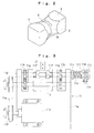
- Figs. 1(a) to 1(f) shows a process for manufacturing a chip resistor in accordance with the present invention.
- Fig. 2 is a perspective view showing an external appearance of the chip resistor manufactured through that process.
- an unburned base element 1 made of ceramic in the shape of a prism as shown in Fig. 1(a) is prepared.
- the base element 1 is formed by extruding ceramic slurry to obtain a rod of a square in cross-section and cutting the rod into a predetermined dimension in turn.
- the ceramic slurry is prepared by mixing a binder, a solvent medium, etc., into alumina particles (70wt% or more).
- a multiplicity of base elements 1 are then introduced into a firing furnace for a provisional burning in a lump under conditions of burning temperature of 100 to 200°C and burning time of 1 to 2 hours to impart thereto a hardness suitable for polishing and grinding which will be described later.
- the base elements 1 After having been preliminarily burned, the base elements 1 are loaded into a barrel polishing machine such as a centrifugal barrel or an eccentric rotary barrel and are polished in a lump. Consequently, principally the edges of the base elements 1 are deburred and rounded. After polishing is completed, detectives are removed by screening or visual inspection to select non-detectives.
- a barrel polishing machine such as a centrifugal barrel or an eccentric rotary barrel
- the polished base elements 1 are then individually grind around their centers to create unit elements 2 each having such a shape as shown in Fig. 1(b).
- the unit element 2 includes prism parts 2a at both ends which are symmetric with respect to its center and an intermediate part 2b between the prism-shaped parts 2a which has a hourglass shape and a cross-sectional shape similarly gradually increasing from its center toward the prism-shaped parts 2a.
- the hourglass-shaped part 2b of the shown example has a circular basic cross section.
- the surface of the hourglass-shaped part 2b is continuous smoothly with the surfaces of the prism-shaped parts 2a by arc boundaries. Specific techniques for this grinding step will be detailed later in connection with a configuration of the apparatus used in that step.
- a multiplicity of unit elements 2 obtained as a result of the grinding operation are then introduced into the firing furnace for proper burning in a lump under conditions of burning temperature of 1300 to 1500°C and burning time of two hours.
- the unit elements 2 are then loaded into the barrel polishing machine such as the centrifugal barrel or the eccentric rotary barrel and are polished in a lump. Consequently, principally the edges of the unit elements 2 are deburred and rounded.
- an even thickness of Ni-Cr based or ruthenium oxide based resistance conductor 3 is formed on the entire surface of the grind unit element 2 by use of thin-film forming techniques such as sputtering or vacuum deposition, or by use of thick-film forming techniques such as paste coating. Since the edges of the unit element 2 have been rounded through the previous polishing step, it is prevented for the edge portions to have a film thickness smaller than the remaining portions.
- the resistor conductor 3 formed on the surface of the unit element 2 is then subjected to trimming for adjusting the resistance value, as shown in Fig. 1(d). More specifically, a groove 3a is formed in the resistance conductor 3 on the hourglass-shaped part 2b while bringing a resistance value detecting terminal into contact with the prism-shaped parts 2a, to perform a regulation of the resistance value.
- the groove 3a may be formed through partial grinding by a grinding blade, or alternatively may be formed through partial melting by means of a laser beam within the infrared region.
- an insulative armor 4 of epoxy resin or silicon glass is formed on the surface of the resistance conductor 3 on the hourglass-shaped part 2b by use of thick-film forming techniques such as paste coating.
- the armor 4 has also an hourglass shape similar to the hourglass-shaped part 2b and has a film thickness gradually decreasing from its center toward its ends. Specific techniques for this armoring step will be described in detail later in connection with a configuration of the apparatus used in that step.
- an even thickness of nickel or Sn-Pb alloy electrode conductor 5 is formed on the surfaces of the prism-shaped parts 2a (each including one end surface and four peripheral surfaces) by use of thin-film forming techniques such as electrolytic plating or non-electrolytic plating.
- the extremities of the electrode conductors 5 may abut against the extremities of the armor 4, or alternatively the former may be adjacent to the latter by slightly spaces. Since the edges of the unit element 2 have been rounded through the previous polishing step, the edge portions are prevented from having a film thickness smaller than the remaining portions. In this manner, the chip resistor as shown in Fig. 2 is manufactured.
- FIG. 3 there is depicted by way of example a unit element manufacturing apparatus which comprises a chuck mechanism generally designated at 11 and a grinding blade 12.
- the chuck mechanism 11 includes a frame 11a, a motor 11b firmly secured to the frame 11a, a transmission shaft 11c rotatably supported on the frame 11a, a belt 11e wound around pulleys 11d on the motor shaft and of the transmission shaft 11c, a pair of chuck shafts 11g rotatably supported on the frame 11a in such a manner that their respective chucks 11f confront each other, and gears 11h for transmitting the rotation of the transmission shaft 11c to the chuck shafts 11g, with confronting faces of the chucks 11f each provided with a circular recess for holding the ends of the base element 1.
- the right-hand chuck shaft 11g in the diagram is transversely movable and is provided with two flanges 11i and 11j.
- a coiled spring 11k, a bearing 11l and an operating ring 11m are rotatably interposed between the two flanges 11i and 11j. And also the operating ring 11m is engaged with a drive arm 11n driven by a drive source not shown.
- the grinding blade 12 on the other hand is comprised of e.g., a diamond blade and is adapted to rotate in a predetermined direction around a rotational shaft parallel to the chuck shafts 11g by a drive source not shown.
- the grinding blade 12 is capable of advancing and retreating orthogonally toward and from the center of rotation of the base element 1 clamped by the chucks 11f.
- the grinding edge of the grinding blade 12 has a rounding corresponding to the shape of the curved surface of the hourglass-shaped part 2b of the unit element 2.
- the drive arm 11n is used to displace the chuck shaft 11g on the displaceable side to the right in the diagram by the operating ring 11m, thereby bringing the chuck 11f at the end of that chuck shaft 11g away from the other chuck 11f to widen the space between the opposed chucks 11f.
- the base element 1 is inserted into the thus widened space between the opposed chucks 11f, and then the chuck shaft 11g on the displaceable side is returned to the shown position, thereby enabling the opposed chucks 11f to clamp the base element 1 therebetween coaxially with the chuck shafts 11g.
- the base element 1 clamped between the opposed chucks 11f can be rotated in a predetermined direction through the transmission of rotation of the motor 11b to the chuck shafts 11g by the pulleys 11d, the belt 11e, the transmission shaft 11c and the gears 11h.
- the grinding blade 12 is gradually advanced toward the rotational axis of the base element 1 to grind the center of the prism-shaped base element 1 into a profile corresponding to the shape of the grinding edge of the grinding blade 12, to produce the unit element 2 having a shape shown in Fig. 1(b).
- the base element 1 can be prevented from sliding on the surfaces of the chucks 11f due to the grinding resistance.
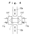
- the base element 1 may be grind by a single grinding blade 12 as mentioned above, a more precise grinding of the base element 1 could be effected by use of two different types of grinding blades with different grinding degrees of roughness, that is, a first blade 12a for rough grinding and a second blade 12b for fine grinding as shown in Fig. 4. It is natural in the case of using a plurality of grinding blades a grinding method may be employed in which maximum grinding depth differs for each blade so that the grinding depth increases stepwise.
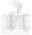
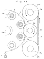
- FIG. 5 there is depicted another example of the unit element manufacturing apparatus which comprises a feeding rotor 21, a relay rotor 22 and a grinding mechanism 23.
- the feeding rotor 21 delivers the base element 1 supplied through a pipe-like chute S to the relay rotor 22 and also as shown in Fig. 6, it includes circumferentially equiangularly spaced receiving grooves 21a (eight at 45 degrees intervals in the diagram) on its periphery.
- Each receiving groove 21a has a substantially square section matching the shape of the end faces of the base element 1 so that a base element 1 supplied sideways through the chute connection point (indicated by a dotted line circle) can be inserted into a receiving groove 21a with the same posture, namely, with its end face forward.
- the feeding rotor 21 includes a curve guide 21b for defining a drop feeding position of the base element 1, and a flat guide 21c for restricting an inserting position of the base element 1 into the receiving guide 21a.
- the relay rotor 22 delivers to a chuck 26 the base element 1 fed from the feeding rotor 21 and also as shown Figs. 6 and 7, it includes circumferentially equiangularly spaced receiving grooves 22a (eight at 45 degrees intervals in the diagram) on its periphery.
- Each receiving groove 22a has a substantially semicircular section larger than the shape of the end faces of the base element 1.
- the relay rotor 22 further includes therewithin a plurality of air suction holes 22b each leading radially to the bottom of the associated receiving groove 22a so that the base element 1 dropped from the feeding rotor 21 can be inserted with the same posture as the above into a receiving groove 22a and sucked by a negative pressure generated by the air suction hole 22b.
- the grinding mechanism 23 includes a frame 24, a pair of right and left chuck wheels 25, a plurality of chucks 26 provided on each of the chuck wheels 25, a couple of belts 27 for rotating the chucks 26, a grinding blade 28 comprised of e.g., a diamond blade, and a chucking control unit 29.
- the pair of chuck wheel 25 are each in the form of a disk with the same shape and are mounted to a shaft 25a secured to the frame 24.
- a rotational drive source such as a motor is connected to the end of the shaft 25a so that during the grinding process the pair of right and left chuck wheels 25 can rotate in the same direction at the same speed.
- the plurality of chucks 26 are arranged circumferentially and equiangularly (eight at 45 degrees intervals in the diagram) and to confront each other on the periphery of each of the chuck wheels 25.
- the chucks 26 on the chuck wheel 25 on the right side in Fig. 5 are attached to the chuck wheel 25 by bearings not shown to rotate around the central axes.
- the chucks 26 on the right-hand chuck wheel 25 are each provided with a pulley part 26a contacted by a belt 27.
- the chucks 26 on the left-hand chuck wheel 25 in Fig. 5 are attached to the chuck wheel 25 by bearings not shown, allowing both rotations around the central axes and transverse movement.
- the chucks 26 on the left-hand chuck wheel 25 are also each provided with a pulley 26a similar to that of the chucks 26 on the other side. Furthermore, the chucks 26 on the left-hand chuck wheels 25 are each biased to the right by a coiled spring 26b in Fig. 5.
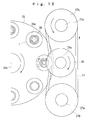
- Each chuck 26 is in the form of a cylindrical member having at its tip a circular recess 26c as shown in Figs. 8(a) to 8(c).
- the chucks 26 on the left side in Fig. 5 are brought nearer or away to enable the two confronting chucks 26 to hold or release the base element 1 in cooperation.
- the chucks 26 arranged on the right-hand chuck wheel 25 in Fig. 5 are each provided with air suction holes 26d leading to the bottom of the recess 26c as shown in Figs. 8(a) to 8(c) so that the base element 1 can be held by a sucking force generated in the air suction hole 2b in addition to a clamping force by the both chucks relatively approaching each other.
- the couple of belts 27 for rotating the chucks selectively rotate the chucks 26 arranged on the chuck wheel 25, and also as shown in Fig. 10 extend vertically adjacent to the chuck wheels 26. More specifically, the belts 27 are vertically wound with a predetermined tension around a driving pulley 27b and a driven pulley 27c which are attached to upper and lower shafts 27a mounted on the frame 24 so as to extend parallel to the shaft 25a, and simultaneously are in partial contact with the pulley parts 26a of the chucks 26 arranged on the right and left chuck wheels 25 of Fig. 5.
- a rotational drive source such as a motor is connected to the end of the shaft 27a associated with the driving pulley 27b so that during the grinding process, the couple of belts can rotate in the same direction at the same speed, causing the chucks 26 contacted by the belts 27 to rotate in the opposite direction.
- the grinding blade 28 grinds the center of the base element 1 retained by the opposed chucks 26, and as shown in Fig. 10, it is attached to the shaft 28a mounted on the frame 24 so as to extend parallel to and level with the shaft 25a.
- the grinding blade 28 is partially positioned between the opposed chucks on the two chuck wheels 25.
- a rotational driving source is connected to the end of the shaft 28a so that during the grinding process which will be described later, the grinding blade 28 can rotate in the opposite direction to that of the chucks 26 at a constant speed.
- the grinding edge of the grinding blade 28 is provided with a rounding corresponding to the profile of the hourglass-shaped part 2b of the unit element 2.
- the chucking control unit 29 imparts a base element holding action to the chucks 26 at the pre-grinding positions and to impart a base element hold releasing action to the chucks 26 at the post-grinding positions.
- the chucking control unit 29 selectively operates the end of the chucks 26 arranged on the chuck wheel 25 on the left side of Figs. 25(a) to 25(d) to thereby control the base element 1 holding action and the hold releasing action. More specifically, as shown in Figs.
- the chucking control unit 29 includes a lever 29a whose one end is engaged with the end of each chuck 26, and a cam plate 29b for pivoting the lever 29a, the cam plate 29b being provided with a raised portion 29c for drawing the chuck 26, over a predetermined angular range (in the shown example, a range short of the base element 1 hold releasing position starting from the base element 1 holding position).
- the end of each lever 29a contacted by the cam plate 29b is provided with a roller 29d for significantly reducing the contact resistance between the lever 29a and the cam plate 29b caused when the chuck wheels 25 rotate.
- the end roller 29d of the lever 29a is pressed by the raised portion 29c of the cam plate 29b, to draw to the left in the diagram the chuck 26 engaging with the other end of the lever 29b against the spring biasing force, to release the holding of the base element 1 (see Fig. 8(a)). Also, by releasing the pressing of the lever 29a against the end roller 29d, the chuck 26 engaging with the other end of the lever 29b can be removed toward the right in the diagram with the aid of the spring biasing force to hold the base element 1 (see Figs. 8(b) and 8(c)).
- the grinding operation continues while gradually increasing the grinding depth of the grinding blade 28 relative to the base element 1 until the center of rotation of the base element 1 becomes level with the center of rotation of the grinding blade 28.
- the grinding operation of the base element 1 by the grinding blade 28 is basically completed when the center of rotation of the base element 1 is coincident in height with the center of rotation of the grinding blade 28.
- the grinding of the base element 1 can be effected by use of a single grinding blade 28 as mentioned above, a plurality of grinding blades having different degrees of roughness may be arranged along a move path (arc trajectory) of the base element 1.
- a plurality of grinding blades having different degrees of roughness may be arranged along a move path (arc trajectory) of the base element 1.
- a grinding method is also possible in which the maximum grinding depth differs for each blade to stepwise increase the grinding depth.
- a type holding and releasing the base element 1 by removing one of the opposed two chucks 26 closer to or away from the other another type of chuck having a clamping feature, e.g., a chuck with claws capable of opening and closing may be employed so that the hold and release of the base element can be carried out on the chuck basis without any need to remove the chuck itself.
- a armoring apparatus which comprises a coating mechanism generally designated at 41 and a modifying roller 42.
- reference numeral 11f denotes a chuck and 11g denote a chuck shaft, which are similar to those of the Fig. 3 apparatus.
- the coating mechanism 41 includes a vessel 41a for storing therein a paste-like armoring material F capable of being hardened, a coating roller 41b whose part is immersed in the armoring material F within the vessel 41a, a blade 41c for scraping down an excess armoring material F adhered to the coating roller 41b, a drive source not shown for rotating the coating roller 41a in a predetermined direction, and another drive source not shown for advancing and retreating the entire apparatus toward and from the unit element 2 held by the chucks 11f.
- the modifying roller 42 removes an excess armoring material F adhered to the resistance conductor 3 on the hourglass-shaped part 2b to modify the adhesion shape and is adapted to rotate in a predetermined direction and to advance and retreat toward and from the unit element 2 held by the chucks 11f.
- the outer peripheral surface of the modifying roller 42 is provided with a rounding corresponding to a shape of the armor 4.
- the armoring material F can be coated on the surface of the resistance conductor 3 on the hourglass-shaped part 2b.
- more armoring material F than needed is coated thereto and hence the adhered armoring material F becomes an hourglass shaped.
- the modifying roller 42 is advanced to the armoring to scrape an excess armoring material F to modify into an hourglass shape.
- a grinding blade 43 for the modification of armor may be advanced to scrape off the excess armoring material F to modify into a hourglass shape.
- a chip resistor as shown in Fig. 2, that is, a chip resistor having an external appearance of prism shape at both ends and of hourglass shape at the center. Since in this chip resistor the electrode conductor 5 is formed on the prism-shaped parts 2a at both ends, one of the side surfaces of the electrode conductor 5 could be utilized as a mounting surface to ensure a stable component mounting onto a substrate or the like while preventing a rolling of the component itself.
- the unit element 2 having a shape shown in Fig. 1(b). Furthermore, by grinding after provisional burning of an unburned ceramic base element 1, the grinding operation is achieved easier and more proper compared with the case in which an unburned base element is grind.
- Fig. 5 ensures that while rotating the base element 1 around its central axis and translating the rotational axis in parallel along the predetermined arc trajectory, the base element 1 is ground around its center by the grinding blade 28 rotating at a position adjacent to the arc trajectory, thereby effecting a desired grinding operation with a gradual increase of grinding depth of the grinding blade 8 relative to the base element 1. Therefore, even when the base element 1 has small dimensions, the initial grinding resistance could be remarkably reduced to securely avoid the problem of occurrence of cracks or fractures, thereby achieving a highly efficient and precise manufacture of the unit element 2 having a desired shape.
- the unit elements 1 held by the chucks 6 can be sequentially fed to the grinding blade 8 side, it would be possible to eliminate time lost in the feeding and hence to significantly reducing a total time needed for the grinding operation, achieving an increased productivity.
- the thickness of the armor 4 could be so modified that the level of the surface of the armor 4 becomes lower than the level of the surface of the electrode conductor 5, while simultaneously enabling the armor 4 to be finished cleanly at a high precision.
- a unit element having a different shape from that of Fig. 1(b) can be simply obtained by altering the shape of the grinding edge or the grinding depth of the grinding blade.
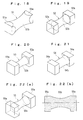
- Figs. 18 to 24 show examples of the shape which can be employed in place of the unit element 2 shown in Fig. 1(b).
- a unit element 51 shown in Fig. 18 has an hourglass-shaped part 51b intervening between prism-shaped parts 51a at both ends.
- the unit element 51 differs in shape from the unit element 2 shown in Fig. 1(b) in that its prism parts 51a are short in length.
- a unit element 52 shown in Fig. 19 has an hourglass-shaped part 52b intervening between prism-shaped parts 52a at both ends.
- the unit element 52 differs in shape from the unit element 2 shown in Fig. 1(b) in that the maximum outer diameter of the hourglass-shaped part 52b is coincident with an inscribed circle of a cross-section of the prism-shaped parts 52a.
- a unit element 53 shown in Fig. 20 has an hourglass-shaped part 53b intervening between prism-shaped parts 53a at both ends.
- the unit element 53 differs in shape from the unit element 2 shown in Fig. 1(b) in that the maximum outer diameter of the hourglass-shaped part 53b is smaller than the diameter of an inscribed circle of a cross-section of the prism-shaped parts 53a.
- a unit element 54 shown in Fig. 21 has an hourglass-shaped part 54b intervening between prism-shaped parts 54a at both ends.
- the unit element 54 differs in shape from the unit element 2 shown in Fig. 1(b) in that the hourglass-shaped part 54b has a cylindrical central portion.
- a unit element 55 shown in Figs. 22(a) and 22(b) has an hourglass-shaped part 51b intervening between prism-shaped parts 51a at both ends.
- the unit element 55 differs in shape from the unit element 2 shown in Fig. 1(b) in that the central axis of the prism-shaped parts 55a at both ends is vertically offset from the central axis of the hourglass-shaped part 55b to impart an eccentric positional relationship to the two parts.
- Fig. 22(a) is a side elevational view of the unit element 55 and Fig. 22(b) is a longitudinal section thereof.
- a unit element 56 shown in Fig. 23 has an hourglass-shaped part 56b intervening between prism-shaped parts 56a at both ends.
- the unit element 55 differs in shape from the unit element 2 shown in Fig. 1(b) in that the hourglass-shaped part 56b has an elliptical reference cross-section.
- a unit element 57 shown in Fig. 24 has an hourglass-shaped part 57b intervening between prism-shaped parts 57a at both ends.
- the unit element 57 differs in shape from the unit element 2 shown in Fig. 1(b) in that the hourglass-shaped part 57b has an elliptical reference cross-section and in that the central axis of the prism-shaped parts 57a at both ends is vertically offset from the central axis at the hourglass-shaped part 57b to impart an eccentric positional relationship to the two parts.
- FIGs. 25(a) to 25(d) there is depicted an embodiment comprising an additional step of forming an interconnection film 6 between the unit element 2 and the resistance conductor 3.
- the other steps are substantially the same as those described with reference to Fig. 1, so an explanation of the other steps is omitted and identical reference numerals are used.
- the film 6 is made of a material which is compatible with both the unit element 2 and the resistance conductor 3 (compatibility in material), for instance, a base metal such as Ni, Cr, Ni-Cr alloy or their alloys.
- the film 6 is formed over the entire surface of the unit element 2 at a thickness of the order of 1 ⁇ m by use of a thin-film forming technique such as sputtering or vacuum deposition. After the formation of the interconnection film 6, the resistance conductor 3 is formed on top of the entire surface of the film 6.
- the intervention of the film 6 made of a material compatible (compatibility in material) with both the unit element 2 and the resistance conductor 3 therebetween contributes to an increase in bonding power exerted between the unit element 2 and the resistance conductor 3. Accordingly, even though a stress is applied to the component during or after mounting thereof, the resistance conductor 3 can be securely prevented from being peeled off from the unit element 2, while ensuring the stable quality and characteristics of the component.
- Fig. 26 shows another embodiment comprising an additional step of partially forming flat areas 4a on top of the surface of the armor 4.
- the other steps are substantially the same as those described with reference to Fig. 1.
- a method of forming the flat areas 4a as shown in Fig. 26 on the surface of the armor 4 includes a method in which a pair of L-shaped templates 61 are pressed against the armoring material F prior to hardening of the coated armoring material F as shown in Figs. 27(a) and 27(b), and a method in which posterior to hardening of the coated armoring material F the surface is partially planed off by a grinding blade.
- the flat areas 4a thus partially formed on the surface of the armor 4 could facilitate the suction of the components by means of a suction nozz le or the like.
- the flat areas 4a may be formed parallel to the surfaces of the electrode conductors 5 lying on the prism-shaped parts, thereby enabling the suction posture to conform to the mounting posture.
- Fig. 28 shows still another embodiment in which the terminal edges of the armor 4 are extended as far as on the prism-shaped parts 2a of the unit element 2, with the electrode conductors 5 being so formed as to abut the terminal edges of the armor 4 or to be adjacent thereto by slightly spaces.
- extension of the terminal edges of the armor 4 as far as on the prism-shaped parts 2a would enable the boundaries between the hourglass-shaped part 2b and the prism-shaped parts 2a to be covered by the armor 4, while simultaneously rendering the shape of the side surfaces of the electrode conductors 5 a perfect rectangle.
- the end edges of the electrode conductors 5 may overlap the end edges of the armor 4 as shown in Fig. 29(a) or 29(b) so that the electrode conductors 5 can prevent the armor 4 from peeling off starting from its end edges.
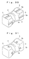
- Figs 30 and 31 shows a still further embodiment in which the surfaces of the electrode conductors 5 are formed with recesses 5a or 5b into which a part of the armor 4 infiltrates. In this case, that the electrode conductor forming step precedes the armor forming step.
- a method of forming the recesses 5a or 5b as shown in Figs. 30 and 31 in the surfaces of the electrode conductors 5 include a partial grinding of the surfaces of the electrode conductors 5 by a grinding blade after the formation of the electrode conductors 5, and a partial removal of the surfaces by the irradiation of laser beam.
- the present invention has been exemplarily applied to a chip resistor which is typical of chip components hereinabove, it is natural that the present invention is not intended to be limited to the chip resistor, but is widely applicable to other chip components, for instance, a chip jumper, a chip inductor, etc., comprised of a unit element which carries thereon a circuit conductor, electrode conductors and an armor.
Abstract
Description
- This invention relates to a method of manufacturing a chip component such as a chip resistor, and to an apparatus for manufacturing a unit element for use in the manufacture of the chip component.
- A cylindrical chip resistor is known as a typical chip component applicable to a chip component feeding apparatus for feeding one by one in a predetermined orientation a multiplicity of chip components accommodated in bulk.
- This chip resistor has a cylindrical ceramic unit element, a resistance conductor formed over the entire surface of the unit element, an armor covering the center of the resistance conductor and a pair of electrode conductors covering the ends of the resistance conductor. The resistance conductor is trimmed with grooves to control the resistance value, if necessary.
- This known chip resistor is no need to orient its obverse and reverse side when it is fed by the apparatus, because its having no obverse and reverse side. But it is liable to roll because of its cylindrical shape, resulting in an unstable mounting onto the substrate or the like and hence in defectiveness such as a positional offset. This inconvenience applies to other similarly shaped chip components than the chip resistor.
- It is a first object of the present invention to provide a new and improved method of manufacturing a chip component ensuring a stable mounting onto a substrate or the like and capable of being applied into a chip component feeding apparatus for feeding one by one in a predetermined orientation chip components accommodated in bulk.
- A second object of the present invention is to provide a new and improved unit element manufacturing apparatus capable of efficiently manufacturing a unit element for use in the manufacture of the chip component described in the first object.
- In order to achieve the first object, according to a first aspect of the present invention, a method of manufacturing a chip component is provided. The method comprises the steps of burning an unburned unit element made of ceramic having prism-shaped parts at its ends; polishing edges of the burned unit element; and forming on the polished unit element a circuit conductor, an electrode conductor and an armor.
- In order to achieve the second object, according to a second aspect of the present invention, an apparatus for manufacturing a unit element for a chip component is provided. The apparatus comprises a chuck for holding a prism-shaped base element in a predetermined orientation to rotate the base element around its central axis or an axis parallel thereto; a chuck wheel for translating the rotational axis of the chuck parallely along a predetermined arc trajectory; and a grinding tool turning at a position adjoining the arc trajectory to grind the center of the base element which is translated parallely in rotation along the arc trajectory.
- These and other related objects, aspects, features and advantages of the present invention will become apparent from the following detailed description in conjunction with the accompanying drawings.
-
- Figs. 1(a) to 1(f) shows a process for manufacturing a chip resistor in accordance with the present invention;
- Fig. 2 is a perspective view showing an external appearance of the chip resistor manufactured through the process shown in Figs. 1(a) to 1(f);
- Fig. 3 shows an example of a unit element manufacturing apparatus for use in a grinding step;
- Fig. 4 shows a variant of the unit element manufacturing apparatus shown in Fig. 3;
- Fig. 5 shows another example of the unit element manufacturing apparatus for use in the grinding step;
- Figs. 6, 7, 8(a), 8(b), 8(c), 9(a), 9(b), 10, 11, 12 and 13 are explanatory views of actions of the unit element manufacturing apparatus shown in Fig. 5;
- Fig. 14 shows a variant of the unit element manufacturing apparatus shown in Fig. 5;
- Fig. 15 shows an example of an armoring apparatus for use in an armoring step;
- Figs. 16(a) and 16(b) shows a technique for the armoring step;
- Fig. 17 shows another technique for the armoring step;
- Figs. 18, 19, 20, 21, 22(a), 22(b), 23 and 24 shows examples of the shape of a unit element replaceable in place of the unit element shown in Fig. 1(b);
- Figs. 25(a) to 25(d) shows an embodiment comprising an additional step of forming an interconnection film between the unit element and a resistance conductor;
- Fig. 26 shows another embodiment comprising an additional step of partially forming flat areas on the surface of the armor;
- Figs. 27(a) and 27(b) shows a technique for partially forming the flat areas on the surface of the armor;
- Fig. 28 shows an embodiment in which the edges of the armor are extended as far as over prism parts of the unit element;
- Figs. 29(a) and 29(b) shows a variant of the case in which the edges of the armor are extended as far as over the prism parts of the unit element;
- Fig. 30 is a diagram showing an embodiment in which the surface of the electrode conductor is provided with recesses into which a part of the armor infiltrates;
- Fig. 31 is a diagram showing another embodiment in which the surface of the electrode conductor is provided with recesses into which a part of the armor infiltrates.
- Figs. 1(a) to 1(f) shows a process for manufacturing a chip resistor in accordance with the present invention. Fig. 2 is a perspective view showing an external appearance of the chip resistor manufactured through that process.
- For the manufacture of the chip resistor shown in Fig. 2, an
unburned base element 1 made of ceramic in the shape of a prism as shown in Fig. 1(a) is prepared. Thebase element 1 is formed by extruding ceramic slurry to obtain a rod of a square in cross-section and cutting the rod into a predetermined dimension in turn. The ceramic slurry is prepared by mixing a binder, a solvent medium, etc., into alumina particles (70wt% or more). - A multiplicity of
base elements 1 are then introduced into a firing furnace for a provisional burning in a lump under conditions of burning temperature of 100 to 200°C and burning time of 1 to 2 hours to impart thereto a hardness suitable for polishing and grinding which will be described later. - After having been preliminarily burned, the
base elements 1 are loaded into a barrel polishing machine such as a centrifugal barrel or an eccentric rotary barrel and are polished in a lump. Consequently, principally the edges of thebase elements 1 are deburred and rounded. After polishing is completed, detectives are removed by screening or visual inspection to select non-detectives. - The polished
base elements 1 are then individually grind around their centers to createunit elements 2 each having such a shape as shown in Fig. 1(b). As is apparent from the figure, theunit element 2 includesprism parts 2a at both ends which are symmetric with respect to its center and anintermediate part 2b between the prism-shaped parts 2a which has a hourglass shape and a cross-sectional shape similarly gradually increasing from its center toward the prism-shaped parts 2a. The hourglass-shaped part 2b of the shown example has a circular basic cross section. The surface of the hourglass-shaped part 2b is continuous smoothly with the surfaces of the prism-shaped parts 2a by arc boundaries. Specific techniques for this grinding step will be detailed later in connection with a configuration of the apparatus used in that step. - A multiplicity of
unit elements 2 obtained as a result of the grinding operation are then introduced into the firing furnace for proper burning in a lump under conditions of burning temperature of 1300 to 1500°C and burning time of two hours. - After the proper burning, the
unit elements 2 are then loaded into the barrel polishing machine such as the centrifugal barrel or the eccentric rotary barrel and are polished in a lump. Consequently, principally the edges of theunit elements 2 are deburred and rounded. - Subsequently, as shown in Fig. 1(c), an even thickness of Ni-Cr based or ruthenium oxide based
resistance conductor 3 is formed on the entire surface of thegrind unit element 2 by use of thin-film forming techniques such as sputtering or vacuum deposition, or by use of thick-film forming techniques such as paste coating. Since the edges of theunit element 2 have been rounded through the previous polishing step, it is prevented for the edge portions to have a film thickness smaller than the remaining portions. - The
resistor conductor 3 formed on the surface of theunit element 2 is then subjected to trimming for adjusting the resistance value, as shown in Fig. 1(d). More specifically, agroove 3a is formed in theresistance conductor 3 on the hourglass-shaped part 2b while bringing a resistance value detecting terminal into contact with the prism-shaped parts 2a, to perform a regulation of the resistance value. Thegroove 3a may be formed through partial grinding by a grinding blade, or alternatively may be formed through partial melting by means of a laser beam within the infrared region. - Subsequently, as shown in Fig. 1(e), an
insulative armor 4 of epoxy resin or silicon glass is formed on the surface of theresistance conductor 3 on the hourglass-shaped part 2b by use of thick-film forming techniques such as paste coating. As can been seen in the figure, thearmor 4 has also an hourglass shape similar to the hourglass-shaped part 2b and has a film thickness gradually decreasing from its center toward its ends. Specific techniques for this armoring step will be described in detail later in connection with a configuration of the apparatus used in that step. - Finally, as shown in Fig. 1(f), an even thickness of nickel or Sn-Pb
alloy electrode conductor 5 is formed on the surfaces of the prism-shaped parts 2a (each including one end surface and four peripheral surfaces) by use of thin-film forming techniques such as electrolytic plating or non-electrolytic plating. The extremities of theelectrode conductors 5 may abut against the extremities of thearmor 4, or alternatively the former may be adjacent to the latter by slightly spaces. Since the edges of theunit element 2 have been rounded through the previous polishing step, the edge portions are prevented from having a film thickness smaller than the remaining portions. In this manner, the chip resistor as shown in Fig. 2 is manufactured. - Detailed description will now be made of a specific technique of the grinding step in connection with a configuration of the apparatus used in that step.
- Referring to Fig. 3 there is depicted by way of example a unit element manufacturing apparatus which comprises a chuck mechanism generally designated at 11 and a grinding
blade 12. - The
chuck mechanism 11 includes aframe 11a, amotor 11b firmly secured to theframe 11a, atransmission shaft 11c rotatably supported on theframe 11a, abelt 11e wound around pulleys 11d on the motor shaft and of thetransmission shaft 11c, a pair ofchuck shafts 11g rotatably supported on theframe 11a in such a manner that theirrespective chucks 11f confront each other, and gears 11h for transmitting the rotation of thetransmission shaft 11c to thechuck shafts 11g, with confronting faces of thechucks 11f each provided with a circular recess for holding the ends of thebase element 1. - The right-
hand chuck shaft 11g in the diagram is transversely movable and is provided with twoflanges coiled spring 11k, a bearing 11l and anoperating ring 11m are rotatably interposed between the twoflanges operating ring 11m is engaged with adrive arm 11n driven by a drive source not shown. - The grinding
blade 12 on the other hand is comprised of e.g., a diamond blade and is adapted to rotate in a predetermined direction around a rotational shaft parallel to thechuck shafts 11g by a drive source not shown. The grindingblade 12 is capable of advancing and retreating orthogonally toward and from the center of rotation of thebase element 1 clamped by thechucks 11f. The grinding edge of the grindingblade 12 has a rounding corresponding to the shape of the curved surface of the hourglass-shapedpart 2b of theunit element 2. - In the
chuck mechanism 11, thedrive arm 11n is used to displace thechuck shaft 11g on the displaceable side to the right in the diagram by theoperating ring 11m, thereby bringing thechuck 11f at the end of thatchuck shaft 11g away from theother chuck 11f to widen the space between theopposed chucks 11f. Thebase element 1 is inserted into the thus widened space between theopposed chucks 11f, and then thechuck shaft 11g on the displaceable side is returned to the shown position, thereby enabling theopposed chucks 11f to clamp thebase element 1 therebetween coaxially with thechuck shafts 11g. Thebase element 1 clamped between theopposed chucks 11f can be rotated in a predetermined direction through the transmission of rotation of themotor 11b to thechuck shafts 11g by thepulleys 11d, thebelt 11e, thetransmission shaft 11c and thegears 11h. - Thus, while the
base element 1 rotates in a predetermined direction, the grindingblade 12 is gradually advanced toward the rotational axis of thebase element 1 to grind the center of the prism-shapedbase element 1 into a profile corresponding to the shape of the grinding edge of the grindingblade 12, to produce theunit element 2 having a shape shown in Fig. 1(b). By shifting theoperating ring 11m to the left in the diagram from the shown position to compress thecoiled spring 11k to increase the clamping pressure applied to thebase element 1, thebase element 1 can be prevented from sliding on the surfaces of thechucks 11f due to the grinding resistance. - Although the
base element 1 may be grind by asingle grinding blade 12 as mentioned above, a more precise grinding of thebase element 1 could be effected by use of two different types of grinding blades with different grinding degrees of roughness, that is, afirst blade 12a for rough grinding and asecond blade 12b for fine grinding as shown in Fig. 4. It is natural in the case of using a plurality of grinding blades a grinding method may be employed in which maximum grinding depth differs for each blade so that the grinding depth increases stepwise. - Referring to Fig. 5, there is depicted another example of the unit element manufacturing apparatus which comprises a feeding
rotor 21, arelay rotor 22 and a grindingmechanism 23. - The feeding
rotor 21 delivers thebase element 1 supplied through a pipe-like chute S to therelay rotor 22 and also as shown in Fig. 6, it includes circumferentially equiangularly spaced receivinggrooves 21a (eight at 45 degrees intervals in the diagram) on its periphery. Each receivinggroove 21a has a substantially square section matching the shape of the end faces of thebase element 1 so that abase element 1 supplied sideways through the chute connection point (indicated by a dotted line circle) can be inserted into a receivinggroove 21a with the same posture, namely, with its end face forward. In the base element delivery area, the feedingrotor 21 includes acurve guide 21b for defining a drop feeding position of thebase element 1, and aflat guide 21c for restricting an inserting position of thebase element 1 into the receivingguide 21a. - The
relay rotor 22 delivers to achuck 26 thebase element 1 fed from the feedingrotor 21 and also as shown Figs. 6 and 7, it includes circumferentially equiangularly spaced receivinggrooves 22a (eight at 45 degrees intervals in the diagram) on its periphery. Each receivinggroove 22a has a substantially semicircular section larger than the shape of the end faces of thebase element 1. Therelay rotor 22 further includes therewithin a plurality of air suction holes 22b each leading radially to the bottom of the associated receivinggroove 22a so that thebase element 1 dropped from the feedingrotor 21 can be inserted with the same posture as the above into a receivinggroove 22a and sucked by a negative pressure generated by theair suction hole 22b. - Referring back to Fig. 5, the grinding
mechanism 23 includes aframe 24, a pair of right and leftchuck wheels 25, a plurality ofchucks 26 provided on each of thechuck wheels 25, a couple ofbelts 27 for rotating thechucks 26, a grindingblade 28 comprised of e.g., a diamond blade, and achucking control unit 29. - The pair of
chuck wheel 25 are each in the form of a disk with the same shape and are mounted to ashaft 25a secured to theframe 24. Although not shown, a rotational drive source such as a motor is connected to the end of theshaft 25a so that during the grinding process the pair of right and leftchuck wheels 25 can rotate in the same direction at the same speed. - The plurality of
chucks 26 are arranged circumferentially and equiangularly (eight at 45 degrees intervals in the diagram) and to confront each other on the periphery of each of thechuck wheels 25. Thechucks 26 on thechuck wheel 25 on the right side in Fig. 5 are attached to thechuck wheel 25 by bearings not shown to rotate around the central axes. Thechucks 26 on the right-hand chuck wheel 25 are each provided with apulley part 26a contacted by abelt 27. On the other hand, thechucks 26 on the left-hand chuck wheel 25 in Fig. 5 are attached to thechuck wheel 25 by bearings not shown, allowing both rotations around the central axes and transverse movement. Thechucks 26 on the left-hand chuck wheel 25 are also each provided with apulley 26a similar to that of thechucks 26 on the other side. Furthermore, thechucks 26 on the left-hand chuck wheels 25 are each biased to the right by acoiled spring 26b in Fig. 5. - Each
chuck 26 is in the form of a cylindrical member having at its tip acircular recess 26c as shown in Figs. 8(a) to 8(c). In the shown example, thechucks 26 on the left side in Fig. 5 are brought nearer or away to enable the two confrontingchucks 26 to hold or release thebase element 1 in cooperation. Thechucks 26 arranged on the right-hand chuck wheel 25 in Fig. 5 are each provided withair suction holes 26d leading to the bottom of therecess 26c as shown in Figs. 8(a) to 8(c) so that thebase element 1 can be held by a sucking force generated in theair suction hole 2b in addition to a clamping force by the both chucks relatively approaching each other. - The couple of
belts 27 for rotating the chucks selectively rotate thechucks 26 arranged on thechuck wheel 25, and also as shown in Fig. 10 extend vertically adjacent to thechuck wheels 26. More specifically, thebelts 27 are vertically wound with a predetermined tension around a drivingpulley 27b and a drivenpulley 27c which are attached to upper andlower shafts 27a mounted on theframe 24 so as to extend parallel to theshaft 25a, and simultaneously are in partial contact with thepulley parts 26a of thechucks 26 arranged on the right and leftchuck wheels 25 of Fig. 5. Although not shown, a rotational drive source such as a motor is connected to the end of theshaft 27a associated with the drivingpulley 27b so that during the grinding process, the couple of belts can rotate in the same direction at the same speed, causing thechucks 26 contacted by thebelts 27 to rotate in the opposite direction. - The grinding
blade 28 grinds the center of thebase element 1 retained by the opposed chucks 26, and as shown in Fig. 10, it is attached to theshaft 28a mounted on theframe 24 so as to extend parallel to and level with theshaft 25a. The grindingblade 28 is partially positioned between the opposed chucks on the twochuck wheels 25. Although not shown, a rotational driving source is connected to the end of theshaft 28a so that during the grinding process which will be described later, the grindingblade 28 can rotate in the opposite direction to that of thechucks 26 at a constant speed. In the same manner as the apparatus shown in Fig. 3, the grinding edge of the grindingblade 28 is provided with a rounding corresponding to the profile of the hourglass-shapedpart 2b of theunit element 2. The chuckingcontrol unit 29 imparts a base element holding action to thechucks 26 at the pre-grinding positions and to impart a base element hold releasing action to thechucks 26 at the post-grinding positions. The chuckingcontrol unit 29 selectively operates the end of thechucks 26 arranged on thechuck wheel 25 on the left side of Figs. 25(a) to 25(d) to thereby control thebase element 1 holding action and the hold releasing action. More specifically, as shown in Figs. 9(a) and 9(b), the chuckingcontrol unit 29 includes alever 29a whose one end is engaged with the end of eachchuck 26, and acam plate 29b for pivoting thelever 29a, thecam plate 29b being provided with a raisedportion 29c for drawing thechuck 26, over a predetermined angular range (in the shown example, a range short of thebase element 1 hold releasing position starting from thebase element 1 holding position). The end of eachlever 29a contacted by thecam plate 29b is provided with aroller 29d for significantly reducing the contact resistance between thelever 29a and thecam plate 29b caused when thechuck wheels 25 rotate. - Thus, in the chucking
control unit 29, theend roller 29d of thelever 29a is pressed by the raisedportion 29c of thecam plate 29b, to draw to the left in the diagram thechuck 26 engaging with the other end of thelever 29b against the spring biasing force, to release the holding of the base element 1 (see Fig. 8(a)). Also, by releasing the pressing of thelever 29a against theend roller 29d, thechuck 26 engaging with the other end of thelever 29b can be removed toward the right in the diagram with the aid of the spring biasing force to hold the base element 1 (see Figs. 8(b) and 8(c)). - As shown in Fig. 6, when a receiving
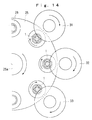
groove 21a of the feedingrotor 21 rotating in the clockwise direction in the diagram is aligned with the chute connection point, thebase element 1 supplied from the pipe-like chute S is inserted into the receivinggroove 21a. When thebase element 1 inserted into the receivinggroove 21a rotates together with the feedingrotor 21 to reach a position right under the rotational shaft, one of the receivinggrooves 22a of therelay rotor 22 rotating in the counterclockwise direction in the diagram is positioned below that position simutaneously, and thebase element 1 is dropped and inserted into the interior of the receivinggroove 22a. Thebase element 1 inserted into the receivinggroove 22a rotates together with therelay rotor 22 while being sucked by the negative pressure in theair suction hole 22b. - As shown in Fig. 7, when the
base element 1 sucked in the receivinggroove 22a rotates together with therelay rotor 22 to reach a position right under the rotational shaft, the opposed chucks 26 on thechuck wheels 25 rotating in the clockwise direction are positioned on both sides of that position (see Fig. 8(a)) simutaneously. Of the twochucks 26 which have reached that position, thechuck 26 on thechuck wheel 25 on the left side of Fig. 5 is removed toward the right in the diagram by the spring biasing force under the action control of the chuckingcontrol unit 29, whereupon thebase element 1 fed to the space between theopposed chucks 26 is clamped and held by the two chucks 26 (see Figs. 8(b) and 8(c)). - As shown in Fig. 10, when
pulley part 26a of thechuck 26 holding thebase element 1 comes into contact with thebelt 27 through the rotation of thechuck wheel 25, thebelt 27 rotating in the counterclockwise direction causes thechuck 26 holding thebase element 1 to start to rotate in the opposite direction (clockwise direction). It is to be noted that at the stage of this start of rotation the grindingblade 28 has not yet come into contact with thebase element 1. - As shown in Fig. 11, when the rotation of the
chuck wheel 25 advances from the state of Fig. 10, the grindingblade 28 rotating in the clockwise direction is retained by the opposed chucks 26 and comes into contact with the center of the rotatingbase element 1 to start the grinding of that portion. - As shown in Fig. 12, when the rotation of the
chuck wheel 25 further advances from the state of Fig. 11, the grinding operation continues while gradually increasing the grinding depth of the grindingblade 28 relative to thebase element 1 until the center of rotation of thebase element 1 becomes level with the center of rotation of the grindingblade 28. In other words, the grinding operation of thebase element 1 by the grindingblade 28 is basically completed when the center of rotation of thebase element 1 is coincident in height with the center of rotation of the grindingblade 28. - As shown in Fig. 13, when the rotation of the
chuck wheel 5 further advances from the state of Fig. 12, thepulley part 26a of the succeedingchuck 26 holding abase element 1 comes into contact with thebelt 27 to exegrinde the grinding operation on the succeedingbase element 1 in the same procedure as the above. When thechucks 26 holding thegrind base element 1 reach a position right under theshaft 25a, thechuck 26 on thechuck wheel 25 on the left side of Fig. 5, of the twochucks 26 which have reached that position, is removed toward the left in the diagram against the spring biasing force under the action control of the chuckingcontrol unit 29, so that the clamping of thebase element 1 by thechucks 26 is released and thebase element 1 drops by gravity into a container or the like disposed below. In this manner, theunit element 2 with the shape shown in Fig. 1(b) can be manufactured. - Although the grinding of the
base element 1 can be effected by use of asingle grinding blade 28 as mentioned above, a plurality of grinding blades having different degrees of roughness may be arranged along a move path (arc trajectory) of thebase element 1. For example, as shown in Fig. 14, there may be arranged in sequence threedifferent grinding blades 31 for rough grinding, 32 for fine grinding and 33 for finish grinding, respectively, or twodifferent grinding blades 31 for rough grinding and 32 for fine grinding, respectively, to thereby subject thebase element 1 to a stepwise grinding operation with different degrees of roughness for more precise grinding. It is natural in the case of using a plurality of grinding blades, a grinding method is also possible in which the maximum grinding depth differs for each blade to stepwise increase the grinding depth. - Although there has exemplarily shown a type holding and releasing the
base element 1 by removing one of the opposed twochucks 26 closer to or away from the other, another type of chuck having a clamping feature, e.g., a chuck with claws capable of opening and closing may be employed so that the hold and release of the base element can be carried out on the chuck basis without any need to remove the chuck itself. - Description will now be made of a specific technique for the above-described armoring step in connection with the configuration of the apparatus used in that step.
- Referring to Fig. 15, there is depicted by example a armoring apparatus which comprises a coating mechanism generally designated at 41 and a modifying
roller 42. In the diagram,reference numeral 11f denotes a chuck and 11g denote a chuck shaft, which are similar to those of the Fig. 3 apparatus. - The
coating mechanism 41 includes avessel 41a for storing therein a paste-like armoring material F capable of being hardened, acoating roller 41b whose part is immersed in the armoring material F within thevessel 41a, ablade 41c for scraping down an excess armoring material F adhered to thecoating roller 41b, a drive source not shown for rotating thecoating roller 41a in a predetermined direction, and another drive source not shown for advancing and retreating the entire apparatus toward and from theunit element 2 held by thechucks 11f. - The modifying
roller 42, on the other hand, removes an excess armoring material F adhered to theresistance conductor 3 on the hourglass-shapedpart 2b to modify the adhesion shape and is adapted to rotate in a predetermined direction and to advance and retreat toward and from theunit element 2 held by thechucks 11f. The outer peripheral surface of the modifyingroller 42 is provided with a rounding corresponding to a shape of thearmor 4. - Thus, by bringing the
coating roller 41b closer to the trimmedunit element 2 which is rotated in a predetermined direction, the armoring material F can be coated on the surface of theresistance conductor 3 on the hourglass-shapedpart 2b. Herein, more armoring material F than needed is coated thereto and hence the adhered armoring material F becomes an hourglass shaped. Accordingly, before hardening of the adhered armoring material F, as shown in Fig. 16(b), the modifyingroller 42 is advanced to the armoring to scrape an excess armoring material F to modify into an hourglass shape. - As an alternative to the above for the formation of the
armor 4, as shown in Fig. 17, after hardening of the adhered armoring material F, a grindingblade 43 for the modification of armor may be advanced to scrape off the excess armoring material F to modify into a hourglass shape. - In this manner, according to a series of manufacturing processes described hereinabove, there is ensured a secure and stable manufacture of such a chip resistor as shown in Fig. 2, that is, a chip resistor having an external appearance of prism shape at both ends and of hourglass shape at the center. Since in this chip resistor the
electrode conductor 5 is formed on the prism-shapedparts 2a at both ends, one of the side surfaces of theelectrode conductor 5 could be utilized as a mounting surface to ensure a stable component mounting onto a substrate or the like while preventing a rolling of the component itself. - Furthermore, by virtue of smoothly continuous boundaries between the prism-shaped
parts 2a and the hourglass-shapedpart 2b which constitute theunit element 2, it will be prevented for the boundaries to have a lower strength than the other portions and hence to be subjected to an occurrence of cracks even though any stress is applied thereto during and after the component mounting. - Also, by grinding the center of the prism-shaped
base element 1, there can be readily obtained theunit element 2 having a shape shown in Fig. 1(b). Furthermore, by grinding after provisional burning of an unburnedceramic base element 1, the grinding operation is achieved easier and more proper compared with the case in which an unburned base element is grind. - Moreover, while rotating the prism-shaped
base element 1, its center is ground by the grindingblade blade base element 1 to ensure a secure and stable acquisition of theunit element 2 having a shape shown in Fig. 1(b). - In addition, through a stepwise grinding operation by the grinding
blades unit element 2 with a higher dimensional precision can be obtained. - Above all, use of the apparatus shown in Fig. 5 ensures that while rotating the
base element 1 around its central axis and translating the rotational axis in parallel along the predetermined arc trajectory, thebase element 1 is ground around its center by the grindingblade 28 rotating at a position adjacent to the arc trajectory, thereby effecting a desired grinding operation with a gradual increase of grinding depth of the grinding blade 8 relative to thebase element 1. Therefore, even when thebase element 1 has small dimensions, the initial grinding resistance could be remarkably reduced to securely avoid the problem of occurrence of cracks or fractures, thereby achieving a highly efficient and precise manufacture of theunit element 2 having a desired shape. - Furthermore, since the
unit elements 1 held by thechucks 6 can be sequentially fed to the grinding blade 8 side, it would be possible to eliminate time lost in the feeding and hence to significantly reducing a total time needed for the grinding operation, achieving an increased productivity. - In addition, because an excess armoring material is removed before or after hardening after the armoring material F onto the surface of the
resistance conductor 3 lying on the hourglass-shapedpart 2b, the thickness of thearmor 4 could be so modified that the level of the surface of thearmor 4 becomes lower than the level of the surface of theelectrode conductor 5, while simultaneously enabling thearmor 4 to be finished cleanly at a high precision. - In the unit element manufacturing apparatus shown in Figs. 3 and 5, a unit element having a different shape from that of Fig. 1(b) can be simply obtained by altering the shape of the grinding edge or the grinding depth of the grinding blade. Figs. 18 to 24 show examples of the shape which can be employed in place of the
unit element 2 shown in Fig. 1(b). - A
unit element 51 shown in Fig. 18 has an hourglass-shapedpart 51b intervening between prism-shapedparts 51a at both ends. Theunit element 51 differs in shape from theunit element 2 shown in Fig. 1(b) in that itsprism parts 51a are short in length. - A
unit element 52 shown in Fig. 19 has an hourglass-shapedpart 52b intervening between prism-shapedparts 52a at both ends. Theunit element 52 differs in shape from theunit element 2 shown in Fig. 1(b) in that the maximum outer diameter of the hourglass-shapedpart 52b is coincident with an inscribed circle of a cross-section of the prism-shapedparts 52a. - A
unit element 53 shown in Fig. 20 has an hourglass-shapedpart 53b intervening between prism-shapedparts 53a at both ends. Theunit element 53 differs in shape from theunit element 2 shown in Fig. 1(b) in that the maximum outer diameter of the hourglass-shapedpart 53b is smaller than the diameter of an inscribed circle of a cross-section of the prism-shapedparts 53a. - A
unit element 54 shown in Fig. 21 has an hourglass-shapedpart 54b intervening between prism-shapedparts 54a at both ends. Theunit element 54 differs in shape from theunit element 2 shown in Fig. 1(b) in that the hourglass-shapedpart 54b has a cylindrical central portion. - A
unit element 55 shown in Figs. 22(a) and 22(b) has an hourglass-shapedpart 51b intervening between prism-shapedparts 51a at both ends. Theunit element 55 differs in shape from theunit element 2 shown in Fig. 1(b) in that the central axis of the prism-shapedparts 55a at both ends is vertically offset from the central axis of the hourglass-shapedpart 55b to impart an eccentric positional relationship to the two parts. Herein, Fig. 22(a) is a side elevational view of theunit element 55 and Fig. 22(b) is a longitudinal section thereof. - A
unit element 56 shown in Fig. 23 has an hourglass-shapedpart 56b intervening between prism-shapedparts 56a at both ends. Theunit element 55 differs in shape from theunit element 2 shown in Fig. 1(b) in that the hourglass-shapedpart 56b has an elliptical reference cross-section. - A unit element 57 shown in Fig. 24 has an hourglass-shaped part 57b intervening between prism-shaped parts 57a at both ends. The unit element 57 differs in shape from the
unit element 2 shown in Fig. 1(b) in that the hourglass-shaped part 57b has an elliptical reference cross-section and in that the central axis of the prism-shaped parts 57a at both ends is vertically offset from the central axis at the hourglass-shaped part 57b to impart an eccentric positional relationship to the two parts. - Referring to Figs. 25(a) to 25(d), there is depicted an embodiment comprising an additional step of forming an
interconnection film 6 between theunit element 2 and theresistance conductor 3. The other steps are substantially the same as those described with reference to Fig. 1, so an explanation of the other steps is omitted and identical reference numerals are used. - The
film 6 is made of a material which is compatible with both theunit element 2 and the resistance conductor 3 (compatibility in material), for instance, a base metal such as Ni, Cr, Ni-Cr alloy or their alloys. Thefilm 6 is formed over the entire surface of theunit element 2 at a thickness of the order of 1 µm by use of a thin-film forming technique such as sputtering or vacuum deposition. After the formation of theinterconnection film 6, theresistance conductor 3 is formed on top of the entire surface of thefilm 6. - Thus, the intervention of the
film 6 made of a material compatible (compatibility in material) with both theunit element 2 and theresistance conductor 3 therebetween contributes to an increase in bonding power exerted between theunit element 2 and theresistance conductor 3. Accordingly, even though a stress is applied to the component during or after mounting thereof, theresistance conductor 3 can be securely prevented from being peeled off from theunit element 2, while ensuring the stable quality and characteristics of the component. - Fig. 26 shows another embodiment comprising an additional step of partially forming
flat areas 4a on top of the surface of thearmor 4. The other steps are substantially the same as those described with reference to Fig. 1. - A method of forming the
flat areas 4a as shown in Fig. 26 on the surface of thearmor 4 includes a method in which a pair of L-shapedtemplates 61 are pressed against the armoring material F prior to hardening of the coated armoring material F as shown in Figs. 27(a) and 27(b), and a method in which posterior to hardening of the coated armoring material F the surface is partially planed off by a grinding blade. - The
flat areas 4a thus partially formed on the surface of thearmor 4 could facilitate the suction of the components by means of a suction nozz le or the like. In this case, theflat areas 4a may be formed parallel to the surfaces of theelectrode conductors 5 lying on the prism-shaped parts, thereby enabling the suction posture to conform to the mounting posture. - Fig. 28 shows still another embodiment in which the terminal edges of the
armor 4 are extended as far as on the prism-shapedparts 2a of theunit element 2, with theelectrode conductors 5 being so formed as to abut the terminal edges of thearmor 4 or to be adjacent thereto by slightly spaces. - Thus, extension of the terminal edges of the
armor 4 as far as on the prism-shapedparts 2a would enable the boundaries between the hourglass-shapedpart 2b and the prism-shapedparts 2a to be covered by thearmor 4, while simultaneously rendering the shape of the side surfaces of theelectrode conductors 5 a perfect rectangle. - Besides, the end edges of the
electrode conductors 5 may overlap the end edges of thearmor 4 as shown in Fig. 29(a) or 29(b) so that theelectrode conductors 5 can prevent thearmor 4 from peeling off starting from its end edges. - Figs 30 and 31 shows a still further embodiment in which the surfaces of the
electrode conductors 5 are formed withrecesses armor 4 infiltrates. In this case, that the electrode conductor forming step precedes the armor forming step. - A method of forming the
recesses electrode conductors 5 include a partial grinding of the surfaces of theelectrode conductors 5 by a grinding blade after the formation of theelectrode conductors 5, and a partial removal of the surfaces by the irradiation of laser beam. - In this manner, by forming the
armor 4 after providing the surfaces of theelectrode conductors 5 with therecesses recesses armor 4 from being locally swelled or from riding onto theelectrode conductors 5, while simultaneously providing effective measures for preventing the level of the surface of thearmor 4 from exceeding the level of the surfaces of theelectrode conductors 5. - Although the present invention has been exemplarily applied to a chip resistor which is typical of chip components hereinabove, it is natural that the present invention is not intended to be limited to the chip resistor, but is widely applicable to other chip components, for instance, a chip jumper, a chip inductor, etc., comprised of a unit element which carries thereon a circuit conductor, electrode conductors and an armor.
Claims (19)
- A method of manufacturing a chip component, comprising the steps of:burning an unburned unit element (2) made of ceramics having prism-shaped parts (2a) at its ends;polishing edges of said burned unit element (2); andforming on said polished unit element (2) a circuit conductor (3), an electrode conductor (5) and an armor (4).
- A method of manufacturing a chip component according to claim 1, further comprising the step of:preparing said unit element (2) by grinding an unburned prism-shaped base element (1) made of ceramics around its center.
- A method of manufacturing a chip component according to claim 2, wherein
said step of preparing said unit element (2) includes, grinding said base element (1) around its center by a grinding tool (12) while rotating said base element (1). - A method of manufacturing a chip component according to claim 2, wherein
said step of preparing said unit element (2) includes, grinding said base element (1) around its center by a grinding tool (28) rotating at a position adjacent to a predetermined arc trajectory while rotating said base element (1) around its central axis or an axis parallel thereto and translating said rotational axis parallely along said arc trajectory. - A method of manufacturing a chip component according to claim 3 or 4, wherein:
said base element (1) is ground by a plurality of grinding tools (12a, 12b, 31-33) each having at least either difference of grinding roughness or grinding depth. - A method of manufacturing a chip component according to one of claims 1 to 5, wherein:
an intermediate part (2b) between said prism-shaped parts (2a) of said unit element (2) has an hourglass shape. - A method of manufacturing a chip component according to claim 6, wherein:
said hourglass-shaped part (2b) has a circular or elliptical basic cross section. - A method of manufacturing a chip component according to claim 6 or 7, wherein:
said prism-shaped parts (2a) and said hourglass-shaped part (2b) have an eccentric relationship. - A method of manufacturing a chip component according to one of claims 1 to 8, wherein:
burning of said unit element (2) is imperfect provisional burning,
said method further comprising the step of:properly burning said unit element (2) whose edges have been polished after said provisional burning. - A method of manufacturing a chip component according to one of claims 1 to 9, further comprising the step of:forming an interconnection film (6) between said unit element (2) and said circuit conductor (3).
- A method of manufacturing a chip component according to one of claims 1 to 10, wherein:
said step of forming said armor (4) on said unit element (2) includes, a step of controlling the thickness of said armor (4) so that the surface level of said armor (4) is lower than the surface level of said electrode conductor (5). - A method of manufacturing a chip component according to claim 11, wherein:
said step of controlling the thickness of said armor (4) includes steps of coating an armor material (F) able to harden and of removing an excess armor material before or after hardening. - A method of manufacturing a chip component according to one of claims 1 to 12, wherein:
said step of forming said armor (4) on said unit element (2) includes, a step of partially forming flat areas (4a) on the surface of said armor (4). - A method of manufacturing a chip component according to one of claims 1 to 13, wherein:
said step of forming said electrode conductor (5) and said armor (4) on said unit element (2) includes, forming said electrode conductor (5) and said armor (4) so that the edge of said armor (4) abut or is slightly spaced apart from the edge of said electrode conductor (5). - A method of manufacturing a chip component according to claim 14, wherein:
the edge of said armor (4) is extended as far as over said prism-shaped parts (2a). - A method of manufacturing a chip component according to claim 14 or 15, wherein:
the surface of said electrode conductor (5) is formed with recess (5a) into which a part of said armor (4) infiltrate. - An apparatus for manufacturing a unit element for a chip component, comprising:a chuck (26) for holding a prism-shaped base element (1) in a predetermined orientation to rotate said base element (1) around its central axis or an axis parallel thereto;a chuck wheel (25) for translating the rotational axis of said chuck (26) parallely along a predetermined arc trajectory; anda grinding tool (28) turning at a position adjoining said arc trajectory to grind the center of said base element (1) which is translated parallely in rotation along said arc trajectory.
- An apparatus for manufacturing a unit element for a chip component according to claim 17, wherein:
said grinding tool includes a plurality of grinding blades (31-33) each having at least either difference of grinding roughness or of grinding depth, and said grinding blades (31-33) being disposed along said arc trajectory. - An apparatus for manufacturing a unit element for a chip component according to claim 17 or 18, further comprising:a chucking controller (29) for imparting to said chuck (26) an action to hold said base element (1) at its pre-grinding position and for imparting to said chuck (26) an action to release the holding of said base element (1) at its post-grinding position.
Applications Claiming Priority (3)
| Application Number | Priority Date | Filing Date | Title |
|---|---|---|---|
| JP290436/96 | 1996-10-31 | ||
| JP29043696 | 1996-10-31 | ||
| JP29043696A JP3466394B2 (en) | 1996-10-31 | 1996-10-31 | Chip component and method of manufacturing the same |
Publications (3)
| Publication Number | Publication Date |
|---|---|
| EP0840332A2 true EP0840332A2 (en) | 1998-05-06 |
| EP0840332A3 EP0840332A3 (en) | 2000-04-19 |
| EP0840332B1 EP0840332B1 (en) | 2007-01-10 |
Family
ID=17756015
Family Applications (1)
| Application Number | Title | Priority Date | Filing Date |
|---|---|---|---|
| EP97118837A Expired - Lifetime EP0840332B1 (en) | 1996-10-31 | 1997-10-29 | Method of manufacturing chip components and apparatus for manufacturing unit elements for chip components |
Country Status (7)
| Country | Link |
|---|---|
| US (2) | US6070787A (en) |
| EP (1) | EP0840332B1 (en) |
| JP (1) | JP3466394B2 (en) |
| KR (1) | KR100269037B1 (en) |
| CN (1) | CN1089938C (en) |
| DE (1) | DE69737224T2 (en) |
| TW (1) | TW391015B (en) |
Cited By (1)
| Publication number | Priority date | Publication date | Assignee | Title |
|---|---|---|---|---|
| GB2362759A (en) * | 1999-12-23 | 2001-11-28 | Ibm | Non Planar Surface for Semiconductor Chips |
Families Citing this family (9)
| Publication number | Priority date | Publication date | Assignee | Title |
|---|---|---|---|---|
| US6918173B2 (en) * | 2000-07-31 | 2005-07-19 | Ceratech Corporation | Method for fabricating surface mountable chip inductor |
| JP4790439B2 (en) * | 2006-02-09 | 2011-10-12 | 富士通株式会社 | Electrodes, electronic components and substrates |
| TWM450811U (en) * | 2012-12-13 | 2013-04-11 | Viking Tech Corp | Electrical resistor element |
| WO2015194353A1 (en) * | 2014-06-18 | 2015-12-23 | 株式会社村田製作所 | Ceramic core burr removing method, burr removing device, and ceramic core manufacturing method |
| US9922770B2 (en) * | 2014-12-26 | 2018-03-20 | Taiyo Yuden Co., Ltd. | Through-type multilayer ceramic capacitor |
| CN107731792A (en) * | 2016-08-10 | 2018-02-23 | 华新科技股份有限公司 | Wafer resistance device and its manufacture method |
| CN107508455A (en) * | 2017-08-25 | 2017-12-22 | 惠科股份有限公司 | Buffer circuit and its display device |
| JP7319811B2 (en) * | 2019-04-01 | 2023-08-02 | Koa株式会社 | Resistor |
| CN114765086A (en) * | 2021-01-12 | 2022-07-19 | 国巨电子(中国)有限公司 | Method for manufacturing resistor |
Citations (2)
| Publication number | Priority date | Publication date | Assignee | Title |
|---|---|---|---|---|
| JPH06290906A (en) * | 1993-03-30 | 1994-10-18 | Taiyo Yuden Co Ltd | Chip resistor and manufacture thereof |
| JPH07307201A (en) * | 1994-03-18 | 1995-11-21 | Taiyo Yuden Co Ltd | Chip component and its manufacture |
Family Cites Families (13)
| Publication number | Priority date | Publication date | Assignee | Title |
|---|---|---|---|---|
| US3676911A (en) * | 1970-11-12 | 1972-07-18 | Frank C Austin | Holding tool |
| FR2365209A1 (en) * | 1976-09-20 | 1978-04-14 | Cii Honeywell Bull | PROCESS FOR THE ASSEMBLY OF MICRO-PLATES OF INTEGRATED CIRCUITS ON A SUBSTRATE AND INSTALLATION FOR ITS IMPLEMENTATION |
| US4313262A (en) * | 1979-12-17 | 1982-02-02 | General Electric Company | Molybdenum substrate thick film circuit |
| JPS62251081A (en) * | 1986-04-23 | 1987-10-31 | Hitachi Ltd | Grinding device and element |
| KR930010116B1 (en) | 1990-10-22 | 1993-10-14 | 한국전기통신공사 | Bicmos semiconductor device and making method of the same |
| US5149662A (en) * | 1991-03-27 | 1992-09-22 | Integrated System Assemblies Corporation | Methods for testing and burn-in of integrated circuit chips |
| US5233327A (en) * | 1991-07-01 | 1993-08-03 | International Business Machines Corporation | Active resistor trimming by differential annealing |
| FR2688629A1 (en) * | 1992-03-10 | 1993-09-17 | Thomson Csf | Method and device for three-dimensional encapsulation of semiconductor chips |
| US5634268A (en) * | 1995-06-07 | 1997-06-03 | International Business Machines Corporation | Method for making direct chip attach circuit card |
| US6118290A (en) * | 1997-06-07 | 2000-09-12 | Tokyo Electron Limited | Prober and method for cleaning probes provided therein |
| JPH1167880A (en) * | 1997-08-18 | 1999-03-09 | Toshiba Mach Co Ltd | Rotary chuck for wafer |
| US6066546A (en) * | 1999-01-08 | 2000-05-23 | Advanced Micro Devices, Inc. | Method to minimize particulate induced clamping failures |
| JP3504543B2 (en) * | 1999-03-03 | 2004-03-08 | 株式会社日立製作所 | Semiconductor device separation method and device, and semiconductor device mounting method |
-
1996
- 1996-10-31 JP JP29043696A patent/JP3466394B2/en not_active Expired - Fee Related
-
1997
- 1997-10-28 TW TW086116100A patent/TW391015B/en not_active IP Right Cessation
- 1997-10-29 US US08/960,368 patent/US6070787A/en not_active Expired - Lifetime
- 1997-10-29 KR KR1019970055782A patent/KR100269037B1/en not_active IP Right Cessation
- 1997-10-29 DE DE69737224T patent/DE69737224T2/en not_active Expired - Fee Related
- 1997-10-29 EP EP97118837A patent/EP0840332B1/en not_active Expired - Lifetime
- 1997-10-29 CN CN97122409A patent/CN1089938C/en not_active Expired - Fee Related
-
2000
- 2000-05-09 US US09/567,325 patent/US6409069B1/en not_active Expired - Fee Related
Patent Citations (2)
| Publication number | Priority date | Publication date | Assignee | Title |
|---|---|---|---|---|
| JPH06290906A (en) * | 1993-03-30 | 1994-10-18 | Taiyo Yuden Co Ltd | Chip resistor and manufacture thereof |
| JPH07307201A (en) * | 1994-03-18 | 1995-11-21 | Taiyo Yuden Co Ltd | Chip component and its manufacture |
Non-Patent Citations (2)
| Title |
|---|
| PATENT ABSTRACTS OF JAPAN vol. 095, no. 001, 28 February 1995 (1995-02-28) & JP 06 290906 A (TAIYO YUDEN CO LTD), 18 October 1994 (1994-10-18) * |
| PATENT ABSTRACTS OF JAPAN vol. 096, no. 003, 29 March 1996 (1996-03-29) & JP 07 307201 A (TAIYO YUDEN CO LTD;OTHERS: 01), 21 November 1995 (1995-11-21) * |
Cited By (3)
| Publication number | Priority date | Publication date | Assignee | Title |
|---|---|---|---|---|
| GB2362759A (en) * | 1999-12-23 | 2001-11-28 | Ibm | Non Planar Surface for Semiconductor Chips |
| US6731012B1 (en) | 1999-12-23 | 2004-05-04 | International Business Machines Corporation | Non-planar surface for semiconductor chips |
| GB2362759B (en) * | 1999-12-23 | 2004-08-25 | Ibm | Non-planar surface for semiconductor chips |
Also Published As
| Publication number | Publication date |
|---|---|
| CN1089938C (en) | 2002-08-28 |
| KR19980033246A (en) | 1998-07-25 |
| JP3466394B2 (en) | 2003-11-10 |
| KR100269037B1 (en) | 2000-10-16 |
| DE69737224T2 (en) | 2007-10-25 |
| EP0840332B1 (en) | 2007-01-10 |
| CN1186309A (en) | 1998-07-01 |
| TW391015B (en) | 2000-05-21 |
| US6409069B1 (en) | 2002-06-25 |
| US6070787A (en) | 2000-06-06 |
| EP0840332A3 (en) | 2000-04-19 |
| DE69737224D1 (en) | 2007-02-22 |
| JPH10135001A (en) | 1998-05-22 |
Similar Documents
| Publication | Publication Date | Title |
|---|---|---|
| EP0840332B1 (en) | Method of manufacturing chip components and apparatus for manufacturing unit elements for chip components | |
| JP4816815B2 (en) | Polishing apparatus for polygonal columnar member and polishing method thereof | |
| JP2517217B2 (en) | Apparatus and method for grinding a surface commutator | |
| JPH1128662A (en) | Working method for tubular ceramic molding | |
| EP0838303B1 (en) | Process and apparatus for chucking and machining an elongated cylindrical article made of a ceramic material | |
| TWI705875B (en) | Grindstone and, method for manufacturing same | |
| US4914872A (en) | Apparatus and method for selectively contouring an airfoil root | |
| EP0642887B1 (en) | Apparatus for producing hollow ground needles | |
| JP3403213B2 (en) | Grooving method and grooving device | |
| EP1611981A1 (en) | Cutting device for thin metallic plate | |
| JP2007237377A (en) | Grooving apparatus and grooving method | |
| JP3418089B2 (en) | Method and apparatus for manufacturing porcelain element for chip component | |
| KR100704689B1 (en) | Sliding contact and method for producing the same | |
| JPH11179641A (en) | Lens centering clamp device and lens centering machine using same | |
| EP1696191A1 (en) | Method of manufacturing an ice making cylinder used for an auger type ice making machine | |
| CN112658912A (en) | Slicing and edging integrated forming machine and working method thereof | |
| JPH01210313A (en) | Slicing device for wafer | |
| JP3466976B2 (en) | Method for crowning a sliding member and apparatus used for the method | |
| JP2004243432A (en) | Cutting method, cutting device, and die producing method | |
| JPH08216021A (en) | Truing method for and manufacture of grinding wheel | |
| JPS5877436A (en) | Lead wire cutting device for print circuit board | |
| JP3601066B2 (en) | Gear honing method with internal gear type honing wheel on gear honing machine | |
| JP2002143173A (en) | Device of producing surgical needle | |
| JPS61166006A (en) | Adjustment for resistance value of film resistor | |
| JPS61166007A (en) | Adjustment for resistance value of film resistor |
Legal Events
| Date | Code | Title | Description |
|---|---|---|---|
| PUAI | Public reference made under article 153(3) epc to a published international application that has entered the european phase |
Free format text: ORIGINAL CODE: 0009012 |
|
| AK | Designated contracting states |
Kind code of ref document: A2 Designated state(s): DE FR GB IT NL |
|
| AX | Request for extension of the european patent |
Free format text: AL;LT;LV;RO;SI |
|
| PUAL | Search report despatched |
Free format text: ORIGINAL CODE: 0009013 |
|
| AK | Designated contracting states |
Kind code of ref document: A3 Designated state(s): AT BE CH DE DK ES FI FR GB GR IE IT LI LU MC NL PT SE |
|
| AX | Request for extension of the european patent |
Free format text: AL;LT;LV;RO;SI |
|
| RIN1 | Information on inventor provided before grant (corrected) |
Inventor name: KAKIUCHI, IKUO Inventor name: TERAOKA, MANABU Inventor name: KURATA, SADAAKI Inventor name: TANBO, KIYOSHI Inventor name: HARADA, SHINISHI |
|
| 17P | Request for examination filed |
Effective date: 20001005 |
|
| AKX | Designation fees paid |
Free format text: DE FR GB IT NL |
|
| 17Q | First examination report despatched |
Effective date: 20040608 |
|
| GRAP | Despatch of communication of intention to grant a patent |
Free format text: ORIGINAL CODE: EPIDOSNIGR1 |
|
| GRAS | Grant fee paid |
Free format text: ORIGINAL CODE: EPIDOSNIGR3 |
|
| GRAA | (expected) grant |
Free format text: ORIGINAL CODE: 0009210 |
|
| AK | Designated contracting states |
Kind code of ref document: B1 Designated state(s): DE FR GB IT NL |
|
| REG | Reference to a national code |
Ref country code: GB Ref legal event code: FG4D |
|
| REF | Corresponds to: |
Ref document number: 69737224 Country of ref document: DE Date of ref document: 20070222 Kind code of ref document: P |
|
| ET | Fr: translation filed | ||
| PLBE | No opposition filed within time limit |
Free format text: ORIGINAL CODE: 0009261 |
|
| STAA | Information on the status of an ep patent application or granted ep patent |
Free format text: STATUS: NO OPPOSITION FILED WITHIN TIME LIMIT |
|
| 26N | No opposition filed |
Effective date: 20071011 |
|
| PG25 | Lapsed in a contracting state [announced via postgrant information from national office to epo] |
Ref country code: IT Free format text: LAPSE BECAUSE OF FAILURE TO SUBMIT A TRANSLATION OF THE DESCRIPTION OR TO PAY THE FEE WITHIN THE PRESCRIBED TIME-LIMIT Effective date: 20070110 |
|
| PGFP | Annual fee paid to national office [announced via postgrant information from national office to epo] |
Ref country code: NL Payment date: 20081021 Year of fee payment: 12 Ref country code: FR Payment date: 20080919 Year of fee payment: 12 |
|
| PGFP | Annual fee paid to national office [announced via postgrant information from national office to epo] |
Ref country code: GB Payment date: 20080916 Year of fee payment: 12 |
|
| PGFP | Annual fee paid to national office [announced via postgrant information from national office to epo] |
Ref country code: DE Payment date: 20081031 Year of fee payment: 12 |
|
| REG | Reference to a national code |
Ref country code: NL Ref legal event code: V1 Effective date: 20100501 |
|
| REG | Reference to a national code |
Ref country code: FR Ref legal event code: ST Effective date: 20100630 |
|
| PG25 | Lapsed in a contracting state [announced via postgrant information from national office to epo] |
Ref country code: NL Free format text: LAPSE BECAUSE OF NON-PAYMENT OF DUE FEES Effective date: 20100501 Ref country code: FR Free format text: LAPSE BECAUSE OF NON-PAYMENT OF DUE FEES Effective date: 20091102 Ref country code: DE Free format text: LAPSE BECAUSE OF NON-PAYMENT OF DUE FEES Effective date: 20100501 |
|
| PG25 | Lapsed in a contracting state [announced via postgrant information from national office to epo] |
Ref country code: GB Free format text: LAPSE BECAUSE OF NON-PAYMENT OF DUE FEES Effective date: 20091029 |