EP0840134B1 - Nachrichtenübertragungsverfahren für eine Testzugriffsportsteuerungsvorrichtung (TAP) - Google Patents
Nachrichtenübertragungsverfahren für eine Testzugriffsportsteuerungsvorrichtung (TAP) Download PDFInfo
- Publication number
- EP0840134B1 EP0840134B1 EP97308311A EP97308311A EP0840134B1 EP 0840134 B1 EP0840134 B1 EP 0840134B1 EP 97308311 A EP97308311 A EP 97308311A EP 97308311 A EP97308311 A EP 97308311A EP 0840134 B1 EP0840134 B1 EP 0840134B1
- Authority
- EP
- European Patent Office
- Prior art keywords
- data
- test
- signal
- chip
- line
- Prior art date
- Legal status (The legal status is an assumption and is not a legal conclusion. Google has not performed a legal analysis and makes no representation as to the accuracy of the status listed.)
- Expired - Lifetime
Links
- 238000012360 testing method Methods 0.000 title claims abstract description 147
- 238000004891 communication Methods 0.000 title claims abstract description 18
- 238000000034 method Methods 0.000 title claims description 11
- 230000001419 dependent effect Effects 0.000 claims description 4
- 230000003111 delayed effect Effects 0.000 abstract 1
- 238000002405 diagnostic procedure Methods 0.000 description 7
- 230000004044 response Effects 0.000 description 6
- 230000000694 effects Effects 0.000 description 5
- 238000012544 monitoring process Methods 0.000 description 5
- 230000001360 synchronised effect Effects 0.000 description 4
- 238000012546 transfer Methods 0.000 description 4
- 230000006870 function Effects 0.000 description 3
- 238000004458 analytical method Methods 0.000 description 2
- 238000013459 approach Methods 0.000 description 2
- 230000003139 buffering effect Effects 0.000 description 2
- MTCFGRXMJLQNBG-UHFFFAOYSA-N serine Chemical compound OCC(N)C(O)=O MTCFGRXMJLQNBG-UHFFFAOYSA-N 0.000 description 2
- 241001522306 Serinus serinus Species 0.000 description 1
- 230000002457 bidirectional effect Effects 0.000 description 1
- 230000005540 biological transmission Effects 0.000 description 1
- 238000006243 chemical reaction Methods 0.000 description 1
- 239000003795 chemical substances by application Substances 0.000 description 1
- 230000001066 destructive effect Effects 0.000 description 1
- 238000011161 development Methods 0.000 description 1
- 230000018109 developmental process Effects 0.000 description 1
- 238000012631 diagnostic technique Methods 0.000 description 1
- 238000010586 diagram Methods 0.000 description 1
- 238000004519 manufacturing process Methods 0.000 description 1
- 230000011664 signaling Effects 0.000 description 1
Images

Classifications
-
- G—PHYSICS
- G01—MEASURING; TESTING
- G01R—MEASURING ELECTRIC VARIABLES; MEASURING MAGNETIC VARIABLES
- G01R31/00—Arrangements for testing electric properties; Arrangements for locating electric faults; Arrangements for electrical testing characterised by what is being tested not provided for elsewhere
- G01R31/28—Testing of electronic circuits, e.g. by signal tracer
- G01R31/317—Testing of digital circuits
- G01R31/3181—Functional testing
- G01R31/3185—Reconfiguring for testing, e.g. LSSD, partitioning
- G01R31/318533—Reconfiguring for testing, e.g. LSSD, partitioning using scanning techniques, e.g. LSSD, Boundary Scan, JTAG
- G01R31/318555—Control logic
-
- G—PHYSICS
- G01—MEASURING; TESTING
- G01R—MEASURING ELECTRIC VARIABLES; MEASURING MAGNETIC VARIABLES
- G01R31/00—Arrangements for testing electric properties; Arrangements for locating electric faults; Arrangements for electrical testing characterised by what is being tested not provided for elsewhere
- G01R31/28—Testing of electronic circuits, e.g. by signal tracer
- G01R31/317—Testing of digital circuits
- G01R31/3181—Functional testing
- G01R31/3185—Reconfiguring for testing, e.g. LSSD, partitioning
- G01R31/318533—Reconfiguring for testing, e.g. LSSD, partitioning using scanning techniques, e.g. LSSD, Boundary Scan, JTAG
- G01R31/318572—Input/Output interfaces
Definitions
- the present invention relates to a test access port controller (TAP controller), and to a method of effecting communication using such a test access port controller.
- TAP controller test access port controller
- the invention is particularly but not exclusively concerned with improving communication in a diagnostic environment between an on-chip embedded target processor and an off-chip host processor.
- Test access port controllers are known in the art. TAP controllers are used to effect communication of test data on and off chip via what is known as a JTAG port.
- the functions of known TAP controllers are defined by IEEE Standard 1149.1 - 1990. That Standard defines test logic which can be included in an integrated circuit to provide standardised approaches to testing the interconnections between integrated circuits, testing the integrated circuit itself, and observing or modifying circuit activities during the integrated circuit's "normal" or "user mode” operation.
- the TAP controller is capable of implementing a variety of different test modes. In each of these test modes, test data is supplied to the chip via an input pin of the TAP controller, and resultant data following the test is supplied off-chip via an output pin of the TAP controller. The resultant data is dependent on the test data and is compared with expected data to check the validity of the test.
- the input and output pins are referred to respectively as TDI and TDO.
- Many existing integrated circuits already incorporate a TAP controller of this type with the input and output pins TDI and TDO.
- the functional circuitry need not be a processor but could be other functional circuitry, which might include a DMA (Direct Memory Access) engine, or on-chip cache.
- DMA Direct Memory Access
- processors were manufactured as a single chip, requiring off-chip access to all their ancillary circuitry, such as memory. As a result, they had a plurality of access pins so that information about the CPU, in particular memory addressing information, was in any event externally available from these access pins.
- chips are more complex and contain not only a processor on-chip but also its associated memory and other ancillary circuitry. Often, there may be more than one processor on a chip, or at least one processor and a DMA (Direct Memory Access) engine or EMI (External Memory Interface) for accessing memory associated with the on-chip processor.
- DMA Direct Memory Access
- EMI Extra Memory Interface
- LSA logic state analyser
- halting the CPU can actually change the way in which the software operates so that a bug which is visible in real time would not be evident if the CPU were halted at that point.
- the monitoring process is slow because it is necessary to wait for a test scan to be completed to allow all of the scan data from the CPU registers to be transmitted off-chip.
- EP 0,636,976 discloses a microprocessor having a JTAG standard boundary scan interface, whereby the JTAG interface is also arranged for controlling direct memory access (DMA) type exchanges via the microprocessor's internal bus.
- DMA direct memory access
- the mode store comprises a register for holding a value in the form of a sequence of bits to denote said one of a test mode and a diagnostic mode of operation.
- the TAP controller can comprise a bypass circuit which allows a continuous data path to be effected between the data input pin and the data output pin, the mode store being capable of holding a value to denote a bypass mode of the test access port controller wherein said continuous data path is effected.
- the invention is particularly applicable to a test access port controller used on an integrated circuit comprising a chain of scan latches, wherein in said test mode a scan test operation is performed.
- the logic circuitry can be operable to supply to on-chip test circuitry a test mode control signal to enable said test circuitry.
- the TAP controller can include a timing control circuit for example in the form of a flip-flop, which alters the timing control between a serial data input stream and a serial data output stream. In the preferred embodiment it alters the timing of incoming serial data streams timed on the positive edges of incoming pulses to an outgoing serial data stream timed from the negative edges of pulses.
- a timing control circuit for example in the form of a flip-flop, which alters the timing control between a serial data input stream and a serial data output stream. In the preferred embodiment it alters the timing of incoming serial data streams timed on the positive edges of incoming pulses to an outgoing serial data stream timed from the negative edges of pulses.
- the TAP controller can hold the identification of an integrated circuit on which the TAP controller is provided.
- the present invention allows a TAP controller which is normally present in any event on an integrated circuit to be used for an additional communication function, that is for the conveying of diagnostic data on and off chip.
- diagnostic data is discussed in more detail in relation to the preferred embodiment, but in essence it allows the integrated circuit to communicate with a host processor to monitor operations of an embedded target processor or other functional circuitry on-chip.
- this can be done without a significant increase in chip overhead (area or pincount).
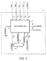
- FIG. 1 illustrates schematically an integrated circuit 2 including a test access port (TAP) controller 4, and a chip boundary scan chain 10.
- the TAP controller 4 receives from off-chip a test clock signal TCK on line 14, a test mode select signal TMS on line 16, a test data input signal TDI on line 18, and a test reset input TRST* on line 22.
- the TAP controller 4 outputs off-chip a test data output signal TDO on line 20.
- the TAP controller 4 also receives a device identifier signal DEVICEID on line 12.
- the signal DEVICEID is shown as a signal line 12 connected, within the integrated circuit, to ground.
- the signal line 12 could be a multi-bit wire, and the signal DEVICEID could originate from either on the integrated circuit or off-chip.
- each bit may be connected either to a logic low level or a logic high level on-chip.
- the TAP controller 4 outputs to on-chip circuitry a scan data input signal SCANIN on line 28, a test clock signal TESTCLK on line 38, a signal indicating selection of a scan test mode SCANMODE on line 24, and a signal indicating selection of a diagnostic mode DIAGMODE on line 26.
- the chip boundary scan chain 10 receives as inputs the scan data input signal SCANIN on line 28 and the signal SCANMODE on line 24, and outputs a scan data output SCANOUT on line 34 to the TAP controller 4.
- the signal SCANIN on line 28 also is connected to on-chip source/destination logic for diagnostic purposes according to the present invention and will be described hereafter.
- the source/destination logic provides an input signal DIAGSCANOUT to the TAP controller 4 on line 36 used in an embodiment of the present invention.
- FIG. 5 illustrates the components that may constitute the source/destination logic.
- the source/destination may at least be a processor connected to an on-chip bus system having on-chip memory connected thereto. Off-chip memory may also be connected directly to such a bus system.
- the on-chip destination/source logic may also include other functional circuitry with a DMA engine or EMI interface.
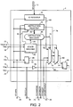
- the TAP controller 4 is illustrated schematically in Figure 2 with those circuit blocks essential to its standard operation and as required by the present invention.
- the TAP controller 4 in basic form, comprises a state machine 50, an ID register 42, an instruction register 44, an instruction decoder 46, a bypass latch 48, a data multiplexor 52, an instruction/data multiplexor 54, a latch 56, and an inverter 60.
- the instruction register receives the test data input signal TDI on line 18, generates a parallel instruction on bus 62 and a serial output on line 76, and receives an instruction control input on line 82.
- the instruction decoder 46 receives the parallel instruction on bus 62 and a decoder control input on line 84, and generates the signals SCANMODE and DIAGMODE on lines 24 and 26 respectively, and a parallel data multiplexor select signal on line 70.
- the bypass latch 48 receives the test data input signal TDI on line 18 and generates an output on line 72.
- the ID register 42 receives the parallel signal DEVICEID on line 12 and generates a serial device identifier output on line 68.
- the data multiplexor 52 receives the output of the ID register 42 on line 68, the output of the bypass latch 48 on line 72, the SCANOUT signal on line 34, the DIAGSCANOUT signal on line 36 and the data multiplexor select signal on line 70.
- the data multiplexor 52 generates an output on line 74.
- the instruction/data multiplexor 54 receives the serial output on line 76, the output of the data multiplexor on line 74, and an instruction/data multiplexor select signal on line 78.
- the instruction/data multiplexor generates an output on line 80.
- the latch 56 receives the output of the instruction/data multiplexor 54 on line 80 and generates the test data output signal TDO on line 20.
- the state machine 50 receives the signal TMS on line 16, and the signal TRST* on line 22.
- the state machine generates the instruction/data multiplexor select signal on line 78, the instruction control input on line 82, and the decoder control input on line 84.
- the latch 56 receives the test clock signal TCK inverted via inverter 60 on line 64.
- the test clock signal TCK and the test data input signal TDI are connected directly as outputs TESTCLK on line 38 and SCANIN on line 28 respectively.
- the TAP controller 4 is a synchronous finite state machine defined by IEEE Standard 1149.1-1990.
- IEEE Standard 1149.1-1990 defines test logic which can be included in an integrated circuit to provide standardised approaches to testing the interconnections between integrated circuits, testing the integrated circuit itself, and observing or modifying circuit activity during the integrated circuit's normal operation.
- the TAP controller 2 During normal operation of the integrated circuit 2, the TAP controller 2 is in a reset state, and all its inputs and outputs are inactive.
- the test access port controller operates according to the definitions of that standard. In such a test mode the test access port controller must be able to select at least one test mode of operation.
- One possible test mode is a scan test mode, which would be selected by setting the signal SCANMODE on line 24. In the scan test mode a scan chain on the integrated circuit 2 is selected for testing. In this example the chip boundary scan chain 10 is selected by the signal SCANMODE.
- Such a scan test may simply involve inputting data in at one end of the scan chain, and checking to see that the same data is output at the other end of the scan chain.
- more complex scan operations may be performed, such as scanning in data which is input to functional logic on-chip, functionally clocking the chip for one or more clock cycles, and then scanning out the outputs of the functional logic.
- Any connection points or circuitry on-chip may be connected for test purposes to form a scan chain.
- the chip boundary scan chain 10 may be a series of flip-flops which are controlled in test mode to connect all the input/output ports of the integrated circuit 2.
- test data output signal TDO is dependent on the test data input signal TDI, and has a time relationship therewith.
- the diagnostic mode of operation is provided for carrying out diagnostic procedures of source/destination logic on-chip, which is compatible with IEEE Standard 1149.1-1990.
- the test data output signal TDO is not dependent on the test data input signal and does not have a time relationship therewith.
- the chain between the test data input signal TDI and the test data output signal TDO is considered to be of infinite length, or open loop.
- the TAP controller whilst continuing to provide all normal functionality, additionally acts as a transport agent carrying full duplex, flow-controlled, unbounded, serial data, although the TAP controller is unaware that this is the form of the data. Conversely the TAP controller normally handles a single stream of data, without any flow control, passing through a selected scan chain.
- Figure 2 shows a mode store in the form of an instruction register 44, data input and output pins in the form of input TDI 18 and output TDO 20 respectively, timing signals in the form of clock signal TCK 14, a switching circuit in the form of multiplexors 52 and 54, and logic circuitry in the form of an instruction decoder 46.
- test data input signal TDI and the test mode select signal TMS are supplied in serial fashion to the TAP controller 4 under control of the test clock signal TCK.
- the state machine 50 acts upon the value of the test mode select signal TMS on each active edge of the test clock signal TCK to cycle through its states accordingly as defined by IEEE Standard 1149.1-1990.
- the test reset signal TRST* provides for asynchronous initialisation of the TAP controller 4 when in a low logic state in accordance with IEEE Standard 1149.1-1990.
- the instruction register 44 is clocked by the test clock signal TCK to load an instruction in serial fashion from the test data input signal TDI under the control of the instruction control input signal on line 82 from the state machine 50.
- the instruction When the instruction has been serially loaded into the instruction register 44, it is transferred in parallel on instruction bus 62 to the instruction decoder 46 under control of the decoder control input signal on line 84 from the state machine 50.
- the instruction decoder will set one of either the SCANMODE signal or the DIAGMODE signal in accordance with whether it is a scan test or a diagnostic test which is to be performed.
- the loading of the instruction register 44 and the instruction decoder 46 are controlled by the state machine 50 in accordance with IEEE Standard 1149.1-1990.
- the parallel output on line 70 of the instruction decoder 46 controls the data multiplexor 52 to connect one of its inputs to the output line 74.
- the output on line 78 of the state machine 50 controls the instruction/data multiplexor to connect one of its inputs to the output on line 80.
- the ID register 42 receives the DEVICEID signal in parallel on lines 12.
- the ID register 42 stores a chip identifier which can be scanned out of the ID register 42 via line 68 to the test data output signal TDO.
- the chip identifier identifes the integrated circuit 2.
- the instruction decoded by the instruction decoder 46 may be simply to output the identity of the device, in which case the multiplexor 52 is controlled to connect its input on line 68 to its output on line 74, and the instruction/data multiplexor 54 is controlled to connect its input on line 74 to its output on line 80. The identity of the device is then serially output as the signal TDO.
- the TAP controller 4 of a particular integrated circuit 2 merely connect the test data input signal TDI to the test data output signal TDO.
- the data multiplexor is controlled to connect the output of the bypass flip-flop on line 72 to the output on line 74, and the instruction/data multiplexor is controlled to connect the line 74 to the output line 80.
- the test data input signal TDI is connected to the test data output signal TDO via the flip-flop 56.
- the latch 56 is merely a flip-flop provided only to allow timing control of the test data output signal TDO so that such signal can be synchronised to the negative edge of the test clock signal TCK.
- test mode to be carried out is a scan test mode
- the instruction decoder 46 sets the signal SCANMODE.
- the data multiplexor 52 is controlled by the instruction decoder 46 to connect the signal SCANOUT to the output line 74.
- the instruction/data multiplexor 54 is also controlled to connect the line 74 to the line 80 so as to output the signal SCANOUT as the test data output signal TDO.
- scan test mode test data is scanned into the selected scan chain on the SCANIN signal which is connected directly to the test data input signal TDI.
- Scan testing in particular boundary scan testing, is fully described in IEEE Standard 1149.1-1990. It will be appreciated that additional control signals, in accordance with the test to be performed, need to be supplied to the selected scan chain to achieve the required test operation.
- a diagnostic mode may also be entered, in which case the instruction decoder 46 sets the signal DIAGMODE on the output line 26. Furthermore, the data multiplexor 52 will be controlled to connect the signal DIAGSCANOUT on line 36 to the output on line 74, which in turn is connected to the line 80 through the instruction/data multiplexor 54 and to the test data output signal TDO via the flip-flop 56.
- the serial data flow between the test data input signal TDI and the test data output signal TDO is be considered to pass through a shift register of infinite length as opposed to the scan test mode, in which mode the serial data flow is through a shift register (shift register chain) of finite length.
- a sequence of bit patterns shifted into the test access port as the test data input signal TDI are never reflected in the sequence of bit patterns shifted out of the test access port as the test data output signal.
- the communication of diagnostic data may include memory access requests from host to target and target to host (reads and writes) ; status information of CPU registers; data read from host memory or target memory in response to a memory access request; status data for loading into CPU registers; and information about memory addresses being accessed by the target CPU.
- the diagnostic mode may involve non-intrusive monitoring of data, or intrusive loading of data.
- the serial data shifted into the test access port is a uni-directional serial data stream which can be encoded in any desired means, for example, with start and stop bits to delineate data chunks.
- data shifted out via the test access port is a uni-directional serial data stream which can be encoded in any desired means, for example with start and stop bits to delineate data chunks.
- the input and output uni-directional data streams may be used simultaneously to allow full-duplex, bidirectional, serial communications.
- the sequence of serial data bits could constitute a byte of information.
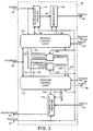
- the integrated circuit 2 when provided with a diagnostic mode of operation in addition to a normal test mode, is preferably provided, as shown in Figure 3, with a data adaptor 90 to interface between the TAP controller 4 and on-chip source/destination logic.
- the data adaptor 90 receives as inputs from the TAP controller 4 the scan data input signal SCANIN on line 28, the test clock signal TESTCLK on line 38 and the signal indicating selection of the diagnostic mode DIAGMODE on line 26.
- the data adaptor 90 outputs to the TAP controller 4 the signal DIAGSCANOUT on line 36.
- the data adaptor receives data from on-chip source/destination logic on a transmit data bus TXDATA on line 92, and outputs data to on-chip source/destination logic on a receive data bus RXDATA on line 94.
- the data adaptor 90 inputs a transmit valid signal TXVALID on line 96, and outputs a transmit acknowledge signal TXACK on line 98, both of which signals are control signals associated with the transmit data bus TXDATA.
- the data adaptor 90 outputs a receive valid signal RXVALID on line 100 and inputs a receive acknowledge signal RXACK on line 102, both of which signals are control signals associated with the receive data bus RXDATA.
- the data adaptor 90 comprises a receive shift register 114, a receive buffer 116, receive control logic 110, a receive flow control status flip-flop 120, a transmit flow control status flip-flop 124, a transmit shift register 118, and transmit control logic 112.
- the receive shift register 114 receives the signal SCANIN on line 28 and a control signal from the receive control logic on line 126, and outputs data in parallel on bus 130 to form an input to the receive buffer 116.
- the receive buffer additionally receives a control signal from the receive control logic on line 128 and generates the receive data bus signal RXDATA on line 94.
- the receive control logic additionally generates the signal RXVALID on line 100, receives the signal RXACK on line 102, receives the signal DIAGMODE on line 26, and generates signals STARTDATA and ACKRX on lines 134 and 132 respectively.
- the receive flow control status flip-flop 120 receives the signal STARTDATA and a signal TXSENDACK on line 136, and outputs a signal RXSENDACK to the transmit control logic on line 142.
- the transmit flow control status flip-flop 124 receives the signal ACKRX and a signal TXSENDBYTE on line 138, and outputs a signal TXWAITACK to the transmit control logic on line 140.
- the transmit control logic 112 additionally receives the signal DIAGMODE on line 26 and the signal TXVALID on line 96, and outputs the signal TXACK on line 98, a control signal to the transmit shift register 118 on line 144, and a parallel signal SERCONT to the transmit shift register 118.
- the transmit shift register 118 additionally receives the parallel data bus TXDATA on lines 92, and outputs the signal DIAGSCANOUT on line 36.
- the data adaptor may optionally be provided with an input from the on-chip system clock, although this connection is not shown in any of the figures.
- the system clock may be used for synchronous implementations where the data and control signals between the data adaptor and the on-chip destination/source logic must be synchronous with the clock of the on-chip destination/source logic.
- the data adaptor 90 performs synchronisation of serial data from the TAP controller clocked by the signal TESTCLK (derived from the signal TCK) to the clock environment of the internal functionality of the destination/source logic, and to the TAP controller clocked by the signal TESTCLK from the clock environment of the internal destination/source logic.
- the TAP controller 4 may optionally provide a scan enable signal to the data adaptor 90, which signal is also not shown in the figures. Such a scan enable signal indicates that the TAP controller has selected this scan path for data output onto the test data output signal TDO.
- the data adaptor converts the uni-directional serial data from off-chip through the TAP controller 2 into a format more suited for use by the on-chip destination/source logic. Conversely the data adaptor must convert the data format supplied by the on-chip destination/scurce logic into unidirectional serial data. In the preferred embodiment, it is desired to provide data to the on-chip destination/source logic in the form of eight parallel bits, or a byte, of data. However, in the extreme the receive data bus RXDATA and the transmit data bus TXBUS could be only one bit, rather than a byte, wide. It is also envisaged that the receive and transmit data buses RXBUS and TXBUS could be multiple byte wide buses.
- the data adaptor 90 must perform the function of "flow control" of both receive and transmit data. Serial data may only be passed through the TAP controller 4 (in either direction) when the receiving end has capacity available to receive that data to prevent data loss or corruption. The communication of the fact that the receiving end is ready to receive more data is achieved by transmitting such information in the reverse direction. This constitutes the flow control protocol.
- the data adaptor 90 according to the described embodiment provides for the unidirectional serial data to be converted into parallel format for communication with the on-chip destination/source logic. Thus a flow control protocol is also necessary between the data adaptor 90 and the on-chip destination/source logic.
- This flow control must thus be performed across two boundaries: the boundary between the TAP controller 4 and the data adaptor 90; and the boundary between the data adaptor 90 and the on-chip destination/source logic to which the data adaptor 90 interfaces.
- the unidirectional data on the test data input signal TDI line and the test data output signal line are encoded with start and stop bits as shown in Figure 4(a).
- the bit flow control protocol is return to zero (RTZ) signalling with two start bits S1 and S2, and a stop bit E1. In between the start bits and the stop bit is included a byte of data.
- Serial data in this format is passed from the test data input TDI of the TAP controller to the SCANIN signal on line 28 and input to the data adaptor 90.
- the receive control logic 110 of the data adaptor receives the serial data signal SCANIN. When the receive control signal recognises two successive serial bits as being the start bits S1 and S2, the receive shift register 114 is controlled on the line 126 to serially load the next eight successive bits, which form a data byte, therein.
- the receive control logic 110 In response to the two consecutive start bits S1 and S2, the receive control logic 110 also sets the signal STARTDATA on line 134, which sets the receive flow control status flip-flop 120.
- the receive flow control status flip-flop 120 sets the signal RXSENDACK on line 142, which signal causes the transmit control logic 112 to send an acknowledgement signal on the test data output signal TDO in the form shown in Figure 4(b), which signal comprises only a start acknowledge bit ACK and a stop bit E1.
- These bits are loaded directly into the transmit shift register in parallel as the signal SERCONT on line 150 under the control of the signal on line 144, and output from the transmit shift register in serial fashion in the form of Figure 4(b), as the signal DIAGSCANOUT.
- the transmit control logic 112 sets the signal TXSENDACK on line 136 to reset the receive flow control status flip-flop and thereby reset the signal RXSENDACK.
- the signal SERCONT in accordance with the flow control protocol used in this embodiment, is a 3 bit signal which enables the start bits S1,S2 and the stop bit E1 to be loaded directly into the transmit shift register 118.
- a byte of data is presented by the on-chip destination logic, to be output through the TAP controller 4, is present on the transmit data bus TXDATA it is loaded in parallel under the control of the transmit control logic 112 into the transmit shift register 118, and the transmit control logic 112 directly loads the start bits S1,S2 and the stop bit E1 forming signal SERCONT into the appropriate bit positions in the transmit shift register prior to serially shifting a signal in the format shown in Figure 4(a).
- the transmit control logic 118 directly loads a single start bit and a stop bit into the transmit shift register, and then serially shifts them out.
- the receive control logic 110 When the receive control logic 110 receives the stop bit E1 on the signal SCANIN, the data byte has been loaded into the receive shift register 114, and under the control of the receive control logic 110 the data byte is transferred on bus 130 from the receive shift register 114 to the receive buffer 116. When a data byte has been loaded into the receive buffer 116 it is output on the bus RXDATA under control of the receive logic 110, which also sets the signal RXVALID on line 100.
- the destination/source logic on-chip responsive to the signal RXVALID, accepts the data byte on the RXBUS and indicates this acceptance by setting the signal RXACK on line 102.
- the receive control logic 110 In response to the signal RXACK the receive control logic 110 resets the signal RXVALID, and if there is a further data byte in the receive shift register 114 transfers this to the receive buffer 116 before again setting the signal RXVALID.
- the receive buffer 116 is provided in the preferred embodiment. This allows acknowledge tokens, which overlap the reception of data, to be transmitted as soon as the two start bits have been received, and this also supports efficient data transfer rates by allowing successive bytes to be transferred without any gap between each byte. Data buffering may also be provided on the transmit side.
- the destination/source logic on-chip transfers data bytes in parallel to the data adaptor 90 on the TXDATA bus 92.
- the signal TXVALID on line 96 is set.
- the transmit control logic controls the transmit shift register 118 via line 144 to load the data byte on the TXDATA bus in parallel.
- the transmit control logic loads the appropriate start bits S1 and S2 and the stop bit E1 into the transmit shift register 118.
- the transmit control logic sets the signal TXACK on line 98 to acknowledge receipt of the data byte to the destination logic on-chip.
- the destination logic on-chip can then transmit a further byte of data.
- Data buffering may be provided in association with the transmit shift register if desired.
- the transmit control logic 112 When the transmit shift register 118 is controlled by the transmit control logic 112 to output serial data in the form shown in Figure 4(a), the transmit control logic 112 also sets the signal TXSENDBYTE on line 138, which sets the transmit flow control status flip-flop 124. In response to this signal, the transmit flow control status flip-flop 124 sets the signal TXWAITACK on line 140. Whilst the TXWAITACK signal is set, the transmit control logic is waiting for an acknowledgement from the destination/source logic off-chip that the data byte set has been received. If the destination/source logic off-chip successfully receives the transmitted data byte than it sends on the test data input signal TDI an acknowledgement signal of the type shown in Figure 4(b).
- the receive control logic 110 Upon receipt of such an acknowledgement signal as the SCANIN signal on line 28, the receive control logic 110 sets the signal ACKRX on line 132, causing the transmit flow control status flip-flop 124, and consequently the signal TXWAITACK, to be reset.
- the transmit control logic 112 is then prepared to receive and transmit the next parallel data byte from the source/destination logic on-chip.
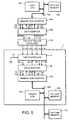
- FIG. 5 illustrates in schematic form how the data adaptor 90 may be used to establish a connection between a host memory and a target memory.
- the integrated circuit 2 comprises the TAP controller 4 and the data adaptor 90 which communicate between each other, off-chip, and with circuitry on-chip using signals as described hereinabove. The same reference numerals are used in Figure 5 to denote signals which correspond to those already described.
- the integrated circuit 2 also comprises a memory bus adaptor 160, a target CPU 162, and an on-chip memory 164.
- the integrated circuit 2 is provided with a memory bus 166 which interfaces with the target CPU 162 and the on-chip memory 164.
- the memory bus 166 is also connected to off-chip memory 174.
- test access port signals TCK,TMS,TDI,TDO and TRST* are connected to a TAP controller initialliser 176, which itself receives a serial data input signal SERIN on line 178 from a further data adaptor 180 and outputs a serial data output signal SEROUT on line 179 to the further data adaptor 180.
- the further data adaptor 180 outputs signals EXTRXDATA, EXTRXVALID, and EXTTXACK on lines 190,188 and 186 respectively to a further memory bus adaptor 194, and receives signals EXTTXDATA, EXTTXVALID, and EXTRXACK on lines 184,182 and 192 respectively from the further memory bus adaptor 194.
- the memory bus adaptor 194 is connected to an external memory bus 198.
- a host CPU 200 is connected to the external memory bus 198 and a further off-chip memory 202 is connected to the external memory bus 198.
- the TAP controller initialiser 176 configures the TAP controller 4 for operation either in the test mode or the diagnostic mode.
- the memory bus adaptors 160 and 194 adapt the parallel data on the bus RXDATA to a message format more suitable for communication with the on-chip destination/source logic.
- the memory bus adaptors are therefore message converters, and may be message converters of the type described in GB Application No. 9622685.7 corresponding to EP 0 840 218.
- the memory bus adaptors must also convert the message format of the on-chip destination/source logic into parallel data bytes for transmission of the bus TXDATA.
- the structure of Figure 5 can be used to implement various diagnostic procedures.
- the serial links on and off chip can allow the communication of various different types of diagnostic data between the integrated circuit 2 and the host CPU 200.
- the host CPU can access the on-chip memory 164 or the off-chip memory 174 using the on-chip bus system 166 but without involving the target CPU 162.
- a memory access request made by the host CPU can be transmitted via the interfacing circuitry comprising the off-chip memory bus adaptor 194, data adaptor 180 and TAP controller initialiser 176 and the on-chip TAP controller 4, data adaptor 90 and memory bus adaptor 160, undergoing the various conversions discussed herein.
- data read from the on-chip memory 164 or off-chip memory 174 can be returned via the on-chip bus system 166 and the interface circuitry to the host CPU.
- the target CPU may access the off-chip memory 202 associated with the host CPU. Data read from the off-chip memory 202 associated with the host CPU 200 can likewise be returned via the interface circuitry.
- the target CPU can be monitored for diagnostic purposes. For example, its accesses to its own memory can be monitored by on-chip circuitry and information about the memory addresses which have been accessed can be transmitted to the host CPU using the interface circuitry.
- the target CPU contains or has access to configuration registers which represent its status. Information about the content of these registers can be transmitted off-chip to the host CPU using the interface circuitry. Conversely, particular status information can be loaded into these registers to affect that state of the target CPU under the instruction of the host CPU.
- the interface circuitry discussed herein allows the communication cf diagnostic data including memory access requests from host to target and target to host (reads and writes) ; status information of CPU registers; data read from host memory or target memory in response to a memory access request; status data for loading into CPU registers; and information about memory addresses being accessed by the target CPU.
- the interface circuitry allows the following diagnostic features to be provided in the circuit:
Landscapes
- Engineering & Computer Science (AREA)
- General Engineering & Computer Science (AREA)
- Physics & Mathematics (AREA)
- General Physics & Mathematics (AREA)
- Test And Diagnosis Of Digital Computers (AREA)
- Tests Of Electronic Circuits (AREA)
- Microcomputers (AREA)
- Maintenance And Management Of Digital Transmission (AREA)
Claims (1)
- Verfahren zum Durchführen von Kommunikation über eine Chipgrenze hinweg, wobei das Verfahren einen Testzugriffsanschluß-Controller auf dem Chip benutzt, wobei der Testzugriffsanschluß-Controller einen JTAG-Testmodus und eine Diagnosebetriebsart aufweist, wobei in dem JTAG-Testmodus ein Testdaten-Ausgabesignal von einem Testdaten-Eingabesignal abhängt und mit jenem in zeitlicher Beziehung steht, wobei das Verfahren umfaßt:Laden von Daten in einen Modusspeicher (44) des Testzugriffsanschluß-Controllers, welche die Diagnosebetriebsart anzeigen;Betätigen eines Schaltkreises (52, 54) des Testzugriffsanschluß-Controllers, um einen Datenausgabeanschluß des Chips zu verbinden, um Diagnosedaten von chipeigenen Schaltkreisen zu empfangen;Erzeugen eines Diagnosemodus-Steuerungssignals, um die Diagnosebetriebsart anzuzeigen, unddadurch gekennzeichnet, daß
in dem Diagnosemodus ein serieller Datenfluß zwischen einem Testdaten-Eingabesignal und einem Testdaten-Ausgabesignal so wie durch ein Schieberegister unendlicher Länge geführt wird, so daß der Testzugriffsanschluß-Controller zur gleichzeitigen Übermittlung der jeweils unabhängigen Testdaten-Eingabesignale und Testdaten-Ausgabesignale auf den Chip und von dem Chip genutzt wird, um die Diagnosedaten zu übertragen, wobei die Testdaten-Eingabesignale und die Testdaten-Ausgabesignale serielle Bitströme sind, wodurch im Diagnosemodus der Testzugriffsanschluß-Controller als Übermittler fungiert, der duplex, flußgesteuerte, unbegrenzte, serielle Daten führt.
Priority Applications (1)
| Application Number | Priority Date | Filing Date | Title |
|---|---|---|---|
| EP07075256A EP1832887A1 (de) | 1996-10-31 | 1997-10-20 | Testzugangsportsteuerung und Verfahren zur Ermöglichung von Kommunikation damit |
Applications Claiming Priority (2)
| Application Number | Priority Date | Filing Date | Title |
|---|---|---|---|
| GBGB9622686.5A GB9622686D0 (en) | 1996-10-31 | 1996-10-31 | A test port controller and a method of effecting communication using the same |
| GB9622686 | 1996-10-31 |
Related Child Applications (1)
| Application Number | Title | Priority Date | Filing Date |
|---|---|---|---|
| EP07075256A Division EP1832887A1 (de) | 1996-10-31 | 1997-10-20 | Testzugangsportsteuerung und Verfahren zur Ermöglichung von Kommunikation damit |
Publications (2)
| Publication Number | Publication Date |
|---|---|
| EP0840134A1 EP0840134A1 (de) | 1998-05-06 |
| EP0840134B1 true EP0840134B1 (de) | 2007-05-16 |
Family
ID=10802229
Family Applications (2)
| Application Number | Title | Priority Date | Filing Date |
|---|---|---|---|
| EP97308311A Expired - Lifetime EP0840134B1 (de) | 1996-10-31 | 1997-10-20 | Nachrichtenübertragungsverfahren für eine Testzugriffsportsteuerungsvorrichtung (TAP) |
| EP07075256A Withdrawn EP1832887A1 (de) | 1996-10-31 | 1997-10-20 | Testzugangsportsteuerung und Verfahren zur Ermöglichung von Kommunikation damit |
Family Applications After (1)
| Application Number | Title | Priority Date | Filing Date |
|---|---|---|---|
| EP07075256A Withdrawn EP1832887A1 (de) | 1996-10-31 | 1997-10-20 | Testzugangsportsteuerung und Verfahren zur Ermöglichung von Kommunikation damit |
Country Status (5)
| Country | Link |
|---|---|
| US (1) | US5983379A (de) |
| EP (2) | EP0840134B1 (de) |
| JP (1) | JP4037494B2 (de) |
| DE (1) | DE69737732T2 (de) |
| GB (1) | GB9622686D0 (de) |
Families Citing this family (70)
| Publication number | Priority date | Publication date | Assignee | Title |
|---|---|---|---|---|
| US6163864A (en) * | 1998-06-10 | 2000-12-19 | Compaq Computer Corporation | Method for cost-effective production testing of input voltage levels of the forwarded clock interface of high performance integrated circuits |
| US6185523B1 (en) * | 1998-10-05 | 2001-02-06 | International Business Machines Corporation | Apparatus and method for computer system interrupt emulation |
| US6158034A (en) * | 1998-12-03 | 2000-12-05 | Atmel Corporation | Boundary scan method for terminating or modifying integrated circuit operating modes |
| FR2790832B1 (fr) * | 1999-03-08 | 2001-06-08 | France Telecom | Procede de test de circuits integres avec acces a des points de memorisation du circuit |
| US6288418B1 (en) * | 1999-03-19 | 2001-09-11 | Nvidia Corporation | Multiuse input/output connector arrangement for graphics accelerator integrated circuit |
| US6711684B1 (en) | 1999-06-08 | 2004-03-23 | General Instrument Corporation | Variable security code download for an embedded processor |
| US7260745B1 (en) | 1999-10-01 | 2007-08-21 | Stmicroelectronics Ltd. | Detection of information on an interconnect |
| US7793261B1 (en) | 1999-10-01 | 2010-09-07 | Stmicroelectronics Limited | Interface for transferring debug information |
| US6629207B1 (en) | 1999-10-01 | 2003-09-30 | Hitachi, Ltd. | Method for loading instructions or data into a locked way of a cache memory |
| US6546480B1 (en) | 1999-10-01 | 2003-04-08 | Hitachi, Ltd. | Instructions for arithmetic operations on vectored data |
| US6351803B2 (en) | 1999-10-01 | 2002-02-26 | Hitachi Ltd. | Mechanism for power efficient processing in a pipeline processor |
| US6408381B1 (en) | 1999-10-01 | 2002-06-18 | Hitachi, Ltd. | Mechanism for fast access to control space in a pipeline processor |
| US6487683B1 (en) | 1999-10-01 | 2002-11-26 | Stmicroelectronics Limited | Microcomputer debug architecture and method |
| US6412047B2 (en) | 1999-10-01 | 2002-06-25 | Stmicroelectronics, Inc. | Coherency protocol |
| US6502210B1 (en) | 1999-10-01 | 2002-12-31 | Stmicroelectronics, Ltd. | Microcomputer debug architecture and method |
| US6460174B1 (en) | 1999-10-01 | 2002-10-01 | Stmicroelectronics, Ltd. | Methods and models for use in designing an integrated circuit |
| US6463553B1 (en) | 1999-10-01 | 2002-10-08 | Stmicroelectronics, Ltd. | Microcomputer debug architecture and method |
| US6542983B1 (en) | 1999-10-01 | 2003-04-01 | Hitachi, Ltd. | Microcomputer/floating point processor interface and method |
| US6665816B1 (en) | 1999-10-01 | 2003-12-16 | Stmicroelectronics Limited | Data shift register |
| US6591369B1 (en) | 1999-10-01 | 2003-07-08 | Stmicroelectronics, Ltd. | System and method for communicating with an integrated circuit |
| US7266728B1 (en) | 1999-10-01 | 2007-09-04 | Stmicroelectronics Ltd. | Circuit for monitoring information on an interconnect |
| US6449712B1 (en) | 1999-10-01 | 2002-09-10 | Hitachi, Ltd. | Emulating execution of smaller fixed-length branch/delay slot instructions with a sequence of larger fixed-length instructions |
| US6557119B1 (en) | 1999-10-01 | 2003-04-29 | Stmicroelectronics Limited | Microcomputer debug architecture and method |
| US6590907B1 (en) | 1999-10-01 | 2003-07-08 | Stmicroelectronics Ltd. | Integrated circuit with additional ports |
| US6918065B1 (en) | 1999-10-01 | 2005-07-12 | Hitachi, Ltd. | Method for compressing and decompressing trace information |
| US6349371B1 (en) | 1999-10-01 | 2002-02-19 | Stmicroelectronics Ltd. | Circuit for storing information |
| US6598128B1 (en) | 1999-10-01 | 2003-07-22 | Hitachi, Ltd. | Microprocessor having improved memory management unit and cache memory |
| US6826191B1 (en) | 1999-10-01 | 2004-11-30 | Stmicroelectronics Ltd. | Packets containing transaction attributes |
| US6553460B1 (en) | 1999-10-01 | 2003-04-22 | Hitachi, Ltd. | Microprocessor having improved memory management unit and cache memory |
| US6530047B1 (en) | 1999-10-01 | 2003-03-04 | Stmicroelectronics Limited | System and method for communicating with an integrated circuit |
| US6298394B1 (en) | 1999-10-01 | 2001-10-02 | Stmicroelectronics, Ltd. | System and method for capturing information on an interconnect in an integrated circuit |
| US6859891B2 (en) | 1999-10-01 | 2005-02-22 | Stmicroelectronics Limited | Apparatus and method for shadowing processor information |
| US6779145B1 (en) | 1999-10-01 | 2004-08-17 | Stmicroelectronics Limited | System and method for communicating with an integrated circuit |
| US6928073B2 (en) * | 1999-10-01 | 2005-08-09 | Stmicroelectronics Ltd. | Integrated circuit implementing packet transmission |
| US6457118B1 (en) | 1999-10-01 | 2002-09-24 | Hitachi Ltd | Method and system for selecting and using source operands in computer system instructions |
| US6567932B2 (en) | 1999-10-01 | 2003-05-20 | Stmicroelectronics Limited | System and method for communicating with an integrated circuit |
| US6772325B1 (en) * | 1999-10-01 | 2004-08-03 | Hitachi, Ltd. | Processor architecture and operation for exploiting improved branch control instruction |
| US6629115B1 (en) | 1999-10-01 | 2003-09-30 | Hitachi, Ltd. | Method and apparatus for manipulating vectored data |
| US6615370B1 (en) | 1999-10-01 | 2003-09-02 | Hitachi, Ltd. | Circuit for storing trace information |
| US6598177B1 (en) | 1999-10-01 | 2003-07-22 | Stmicroelectronics Ltd. | Monitoring error conditions in an integrated circuit |
| US6574651B1 (en) | 1999-10-01 | 2003-06-03 | Hitachi, Ltd. | Method and apparatus for arithmetic operation on vectored data |
| US6633971B2 (en) | 1999-10-01 | 2003-10-14 | Hitachi, Ltd. | Mechanism for forward data in a processor pipeline using a single pipefile connected to the pipeline |
| US6601189B1 (en) | 1999-10-01 | 2003-07-29 | Stmicroelectronics Limited | System and method for communicating with an integrated circuit |
| JP2001142692A (ja) * | 1999-10-01 | 2001-05-25 | Hitachi Ltd | 2つの異なる固定長命令セットを実行するマイクロプロセッサ、マイクロコンピュータおよび命令実行方法 |
| US6684348B1 (en) | 1999-10-01 | 2004-01-27 | Hitachi, Ltd. | Circuit for processing trace information |
| US6820195B1 (en) | 1999-10-01 | 2004-11-16 | Hitachi, Ltd. | Aligning load/store data with big/little endian determined rotation distance control |
| US7072817B1 (en) * | 1999-10-01 | 2006-07-04 | Stmicroelectronics Ltd. | Method of designing an initiator in an integrated circuit |
| US6701405B1 (en) | 1999-10-01 | 2004-03-02 | Hitachi, Ltd. | DMA handshake protocol |
| US6412043B1 (en) | 1999-10-01 | 2002-06-25 | Hitachi, Ltd. | Microprocessor having improved memory management unit and cache memory |
| US6732307B1 (en) | 1999-10-01 | 2004-05-04 | Hitachi, Ltd. | Apparatus and method for storing trace information |
| US6693914B1 (en) | 1999-10-01 | 2004-02-17 | Stmicroelectronics, Inc. | Arbitration mechanism for packet transmission |
| US6434665B1 (en) | 1999-10-01 | 2002-08-13 | Stmicroelectronics, Inc. | Cache memory store buffer |
| US7000078B1 (en) | 1999-10-01 | 2006-02-14 | Stmicroelectronics Ltd. | System and method for maintaining cache coherency in a shared memory system |
| US6848068B1 (en) * | 2000-06-07 | 2005-01-25 | Cypress Semiconductor Corp. | Soft coding of multiple device IDs for IEEE compliant JTAG devices |
| US7168032B2 (en) * | 2000-12-15 | 2007-01-23 | Intel Corporation | Data synchronization for a test access port |
| EP1293790B1 (de) | 2001-09-18 | 2006-12-20 | STMicroelectronics Limited | Abfrageprüfgerät, das Überabtastung zur Synchronisierung verwendet |
| US7571068B2 (en) * | 2002-08-14 | 2009-08-04 | Nxp B.V. | Module, electronic device and evaluation tool |
| KR100626375B1 (ko) * | 2003-07-21 | 2006-09-20 | 삼성전자주식회사 | 고주파로 동작하는 반도체 메모리 장치 및 모듈 |
| US7149933B2 (en) * | 2003-08-07 | 2006-12-12 | Arm Limited | Data processing system trace bus |
| US7818640B1 (en) | 2004-10-22 | 2010-10-19 | Cypress Semiconductor Corporation | Test system having a master/slave JTAG controller |
| ATE534077T1 (de) * | 2005-02-24 | 2011-12-15 | Microchip Tech Inc | Aktivierung von sondermodi bei einer digitalen vorrichtung |
| CN1963778A (zh) * | 2005-11-11 | 2007-05-16 | 鸿富锦精密工业(深圳)有限公司 | 主板串口测试系统及方法 |
| US7814386B2 (en) * | 2007-10-31 | 2010-10-12 | Texas Instruments Incorporated | Built in self test for input/output characterization |
| DE102009012768B4 (de) * | 2009-03-12 | 2021-12-30 | Texas Instruments Deutschland Gmbh | JTAG Nachrichtenbox |
| US8151149B2 (en) * | 2009-06-29 | 2012-04-03 | Hynix Semiconductor Inc. | Semiconductor memory apparatus and method of testing the same |
| US8914693B2 (en) * | 2012-02-15 | 2014-12-16 | International Business Machines Corporation | Apparatus for JTAG-driven remote scanning |
| KR102010454B1 (ko) * | 2012-12-26 | 2019-08-13 | 삼성전자주식회사 | 스캔 플립-플롭, 이의 동작 방법, 및 이를 포함하는 데이터 처리 장치 |
| US20170053088A1 (en) * | 2015-08-22 | 2017-02-23 | Muses Labs, Inc. | Interactive and analytical mobile system that provides a dynamic tool for therapies to prevent and change the progression of dementia-related diseases |
| US11257593B2 (en) | 2014-01-29 | 2022-02-22 | Umethod Health, Inc. | Interactive and analytical system that provides a dynamic tool for therapies to prevent and cure dementia-related diseases |
| CN111929562B (zh) * | 2020-07-03 | 2023-06-23 | 上海美仁半导体有限公司 | 芯片测试系统、测试方法、芯片的测试响应方法和芯片 |
Citations (1)
| Publication number | Priority date | Publication date | Assignee | Title |
|---|---|---|---|---|
| EP0840217A1 (de) * | 1996-10-31 | 1998-05-06 | STMicroelectronics Limited | Eine integrierte Schaltung mit einer TAP (Testzugriffport) Steuerungsvorrichtung |
Family Cites Families (8)
| Publication number | Priority date | Publication date | Assignee | Title |
|---|---|---|---|---|
| US5423050A (en) * | 1991-11-27 | 1995-06-06 | Ncr Corporation | Intermodule test across system bus utilizing serial test bus |
| US5448576A (en) * | 1992-10-29 | 1995-09-05 | Bull Hn Information Systems Inc. | Boundary scan architecture extension |
| US5627842A (en) * | 1993-01-21 | 1997-05-06 | Digital Equipment Corporation | Architecture for system-wide standardized intra-module and inter-module fault testing |
| EP0636976B1 (de) * | 1993-07-28 | 1998-12-30 | Koninklijke Philips Electronics N.V. | Mikrokontroller mit hardwaremässiger Fehlerbeseitigungsunterstützung nach dem Boundary-Scanverfahren |
| GB9417602D0 (en) * | 1994-09-01 | 1994-10-19 | Inmos Ltd | A controller for implementing scan testing |
| US5570375A (en) * | 1995-05-10 | 1996-10-29 | National Science Council Of R.O.C. | IEEE Std. 1149.1 boundary scan circuit capable of built-in self-testing |
| GB9617033D0 (en) * | 1996-08-14 | 1996-09-25 | Int Computers Ltd | Diagnostic memory access |
| US5771240A (en) * | 1996-11-14 | 1998-06-23 | Hewlett-Packard Company | Test systems for obtaining a sample-on-the-fly event trace for an integrated circuit with an integrated debug trigger apparatus and an external pulse pin |
-
1996
- 1996-10-31 GB GBGB9622686.5A patent/GB9622686D0/en active Pending
-
1997
- 1997-10-20 EP EP97308311A patent/EP0840134B1/de not_active Expired - Lifetime
- 1997-10-20 DE DE69737732T patent/DE69737732T2/de not_active Expired - Lifetime
- 1997-10-20 EP EP07075256A patent/EP1832887A1/de not_active Withdrawn
- 1997-10-29 US US08/960,007 patent/US5983379A/en not_active Expired - Lifetime
- 1997-10-31 JP JP30108397A patent/JP4037494B2/ja not_active Expired - Lifetime
Patent Citations (1)
| Publication number | Priority date | Publication date | Assignee | Title |
|---|---|---|---|---|
| EP0840217A1 (de) * | 1996-10-31 | 1998-05-06 | STMicroelectronics Limited | Eine integrierte Schaltung mit einer TAP (Testzugriffport) Steuerungsvorrichtung |
Also Published As
| Publication number | Publication date |
|---|---|
| DE69737732T2 (de) | 2008-02-14 |
| US5983379A (en) | 1999-11-09 |
| EP1832887A1 (de) | 2007-09-12 |
| GB9622686D0 (en) | 1997-01-08 |
| JPH10187477A (ja) | 1998-07-21 |
| JP4037494B2 (ja) | 2008-01-23 |
| DE69737732D1 (de) | 2007-06-28 |
| EP0840134A1 (de) | 1998-05-06 |
Similar Documents
| Publication | Publication Date | Title |
|---|---|---|
| EP0840134B1 (de) | Nachrichtenübertragungsverfahren für eine Testzugriffsportsteuerungsvorrichtung (TAP) | |
| EP0840217B1 (de) | Eine integrierte Schaltung mit einer TAP (Testzugriffport) Steuerungsvorrichtung | |
| EP0840219B1 (de) | Integrierte Halbleiterspeicheranordnung und Kommunikationsverfahren dafür | |
| EP0982595B1 (de) | Integrierte Schaltung mit mehreren Prozessorkernen | |
| EP0840220B1 (de) | Integrierte Halbleiterspeicheranordnung und Kommunikationsverfahren dafür | |
| EP0849670B1 (de) | Integrierter Rechner mit Befehlsverfolgung | |
| EP0849669B1 (de) | Diagnosesystem und Verfahren bei einer integrierten Schaltung | |
| EP0849668B1 (de) | Diagnosesystem und Verfahren bei einer integrierten Halbleiterschaltung | |
| EP0862115B1 (de) | Steuervorrichtung einer Auslösesignalreihenfolge | |
| EP0840218B1 (de) | Integrierte Halbleiterspeicheranordnung und Kommunikationsverfahren dafür | |
| EP0840235B1 (de) | Nachrichtenprotokoll | |
| US8225155B2 (en) | JTAG mailbox | |
| US6381721B1 (en) | Detecting communication errors across a chip boundary |
Legal Events
| Date | Code | Title | Description |
|---|---|---|---|
| PUAI | Public reference made under article 153(3) epc to a published international application that has entered the european phase |
Free format text: ORIGINAL CODE: 0009012 |
|
| AK | Designated contracting states |
Kind code of ref document: A1 Designated state(s): DE FR GB IT |
|
| AX | Request for extension of the european patent |
Free format text: AL;LT;LV;RO;SI |
|
| 17P | Request for examination filed |
Effective date: 19981028 |
|
| AKX | Designation fees paid |
Free format text: DE FR GB IT |
|
| RBV | Designated contracting states (corrected) |
Designated state(s): DE FR GB IT |
|
| RAP3 | Party data changed (applicant data changed or rights of an application transferred) |
Owner name: STMICROELECTRONICS LIMITED |
|
| 17Q | First examination report despatched |
Effective date: 20040823 |
|
| GRAP | Despatch of communication of intention to grant a patent |
Free format text: ORIGINAL CODE: EPIDOSNIGR1 |
|
| RTI1 | Title (correction) |
Free format text: A METHOD OF EFFECTING COMMUNICATION USING A TEST ACCESS PORT (TAP) CONTROLLER |
|
| GRAS | Grant fee paid |
Free format text: ORIGINAL CODE: EPIDOSNIGR3 |
|
| GRAA | (expected) grant |
Free format text: ORIGINAL CODE: 0009210 |
|
| AK | Designated contracting states |
Kind code of ref document: B1 Designated state(s): DE FR GB IT |
|
| REG | Reference to a national code |
Ref country code: GB Ref legal event code: FG4D |
|
| REF | Corresponds to: |
Ref document number: 69737732 Country of ref document: DE Date of ref document: 20070628 Kind code of ref document: P |
|
| ET | Fr: translation filed | ||
| PLBE | No opposition filed within time limit |
Free format text: ORIGINAL CODE: 0009261 |
|
| STAA | Information on the status of an ep patent application or granted ep patent |
Free format text: STATUS: NO OPPOSITION FILED WITHIN TIME LIMIT |
|
| 26N | No opposition filed |
Effective date: 20080219 |
|
| REG | Reference to a national code |
Ref country code: FR Ref legal event code: PLFP Year of fee payment: 20 |
|
| PGFP | Annual fee paid to national office [announced via postgrant information from national office to epo] |
Ref country code: GB Payment date: 20160928 Year of fee payment: 20 |
|
| PGFP | Annual fee paid to national office [announced via postgrant information from national office to epo] |
Ref country code: FR Payment date: 20160921 Year of fee payment: 20 |
|
| PGFP | Annual fee paid to national office [announced via postgrant information from national office to epo] |
Ref country code: DE Payment date: 20160922 Year of fee payment: 20 |
|
| PGFP | Annual fee paid to national office [announced via postgrant information from national office to epo] |
Ref country code: IT Payment date: 20160923 Year of fee payment: 20 |
|
| REG | Reference to a national code |
Ref country code: DE Ref legal event code: R071 Ref document number: 69737732 Country of ref document: DE |
|
| REG | Reference to a national code |
Ref country code: GB Ref legal event code: PE20 Expiry date: 20171019 |
|
| PG25 | Lapsed in a contracting state [announced via postgrant information from national office to epo] |
Ref country code: GB Free format text: LAPSE BECAUSE OF EXPIRATION OF PROTECTION Effective date: 20171019 |