EP0982595B1 - Integrierte Schaltung mit mehreren Prozessorkernen - Google Patents
Integrierte Schaltung mit mehreren Prozessorkernen Download PDFInfo
- Publication number
- EP0982595B1 EP0982595B1 EP99306192A EP99306192A EP0982595B1 EP 0982595 B1 EP0982595 B1 EP 0982595B1 EP 99306192 A EP99306192 A EP 99306192A EP 99306192 A EP99306192 A EP 99306192A EP 0982595 B1 EP0982595 B1 EP 0982595B1
- Authority
- EP
- European Patent Office
- Prior art keywords
- chip
- data
- signal
- integrated circuit
- message
- Prior art date
- Legal status (The legal status is an assumption and is not a legal conclusion. Google has not performed a legal analysis and makes no representation as to the accuracy of the status listed.)
- Expired - Lifetime
Links
Images


Classifications
-
- G—PHYSICS
- G06—COMPUTING; CALCULATING OR COUNTING
- G06F—ELECTRIC DIGITAL DATA PROCESSING
- G06F11/00—Error detection; Error correction; Monitoring
- G06F11/22—Detection or location of defective computer hardware by testing during standby operation or during idle time, e.g. start-up testing
- G06F11/26—Functional testing
- G06F11/267—Reconfiguring circuits for testing, e.g. LSSD, partitioning
Definitions
- This invention relates to an integrated circuit, and particularly an integrated circuit with multiple processing cores and which includes a test access port controller (TAP controller) for effecting communication of serial data across the chip boundary.
- TAP controller test access port controller
- Test access port controllers are known in the art. TAP controllers are used to effect communication of test data on and off chip via what is known as a JTAG port.
- the functions of known TAP controllers are defined by IEEE Standard 1149.1 - 1990. That Standard defines test logic which can be included in an integrated circuit to provide standardised approaches to testing the interconnections between integrated circuits, testing the integrated circuit itself, and observing or modifying circuit activities during the integrated circuit's "normal" or "user mode” operation.
- the TAP controller is capable of implementing a variety of different test modes. In each of these test modes, test data is supplied to the chip via an input pin of the TAP controller, and resultant data following the test is supplied off-chip via an output pin of the TAP controller. The resultant data is dependent on the test data and is compared with expected data to check the validity of the test.
- the input and output pins are referred to respectively as TDI and TDO.
- Many existing integrated circuits already incorporate a TAP controller of this type with the input and output pins TDI and TDO.
- the functional circuitry need not be a processor but could be other functional circuitry, which might include a DMA (Direct Memory Access) engine, or on-chip cache.
- DMA Direct Memory Access
- processors were manufactured as a single chip, requiring off-chip access to all their ancillary circuitry, such as memory. As a result, they had a plurality of access pins so that information about the CPU, in particular memory addressing information, was in any event externally available from these access pins.
- EP-A-0840217 provides a system which greatly simplifies debugging for an integrated circuit with an on-chip processor.
- it is desirable to debug each core preferably as independently as possible.
- debugging software which runs on a host and which controls the debugging process is different and independent for each target processing core. This is difficult to implement with the system described in EP-A-0840217 because all on and off-chip communications take place via the TAP controller which responds to instructions from a single source only.
- the earlier system does allow for on-chip functionality which comprises more than one processing core, the problem of independence required between the diagnostic facilities for each core and the independence of communication between each diagnostic facility and the corresponding independent software module on the host is not addressed.
- the present invention seeks to provide a system which will accommodate this.
- an integrated circuit comprising: a) a serial data input pin and a serial data output pin; b) on-chip functional circuitry comprising at least two processing cores; c) a data adaptor which is in communication with the processing cores by respective communication channels and is arranged to be connected to the input and output pins, characterised in that the data adaptor comprises: i) transmit circuitry including means for receiving first parallel data and control signals from said on-chip functional circuitry, and ii) means for converting said first parallel data and control signals into a first sequence of serial bits including flow control bits, data bits and channel identification bits which identify the communication channel on which said parallel data and control signals were received, and iii) receive circuitry including means for receiving from off-chip via the serial data input pin a second sequence of serial bits including flow control bits, data bits and channel identification bits, iv) means for converting said second sequence into second parallel data and control signals for said on-chip functional circuitry; and v) means for transmitting said second parallel data
- the receive circuitry comprises decoding means for decoding an event sequence of said serial bits, said event sequence including said channel identification bits.
- the event sequence can comprise an event header constituting a data packet.
- the transmit circuitry can include an event generator which generates an event sequence of bits to identify the communication channel on which data is being transmitted. An event can be generated when the instant communication channel is switched to an alternative communication channel.
- Each processing core preferably includes at least one autonomously operating processor.
- it can also include on-chip memory and a bus system for communicating with said on-chip memory and also possibly with off-chip memory.
- each processing core can include a message converter which formulates messages to be transmitted off-chip via the data adaptor and decodes messages which are received on-chip via the data adaptor.
- each processing core can comprise a set of registers holding information for diagnostic purposes, said registers being accessible from off-chip via the data adaptor and the communication channel associated with that processing core. This allows simultaneous independent debugging of on-chip independent processing cores to be accomplished.
- the integrated circuit can comprise a test access port controller connected to effect communication of serial data across the chip boundary via said input and output pins, the test access port controller being connectable to on-chip test logic in a first mode of operation and connectable to the data adaptor in a second mode of operation.
- the invention also provides a number of different computer systems incorporating an integrated circuit as above defined.
- two independently operating off-chip processors are connected to the chip by an off-chip host communications adaptor for independently debugging two on-chip processing cores.
- an off-chip host processor has two independently running debugging applications which can communicate independently via an off-chip adaptor with two on-chip independent processing cores.
- an off-chip host processor executes a debugging application with independently operable interface modules which can communicate independently with on-chip processing cores via an off-chip host adaptor.
- the invention also provides a method of effecting communication of messages from one of a plurality of independent processing cores on an integrated circuit to an off-chip host processor, wherein:
- FIG. 1 illustrates schematically an integrated circuit 2 including a test access port (TAP) controller 4, and a chip boundary scan chain 10.
- the TAP controller 4 receives from off-chip a test clock signal TCK on line 14, a test mode select signal TMS on line 16, a test data input signal TDI on line 18, and a test reset input TRST* on line 22.
- the TAP controller 4 outputs off-chip a test data output signal TDO on line 20.
- the TAP controller 4 also receives a device identifier signal DEVICEID on line 12.
- the signal DEVICEID is shown as a signal line 12 connected, within the integrated circuit, to ground.
- the signal line 12 could be a multi-bit wire, and the signal DEVICEID could originate from either on the integrated circuit or off-chip.
- each bit may be connected either to a logic low level or a logic high level on chip.
- the TAP controller 4 outputs to on-chip circuitry a scan data input signal SCANIN on line 28, a test clock signal TESTCLK on line 38, a signal indicating selection of a scan test mode SCANMODE on line 24, and a signal indicating selection of a diagnostic mode DIAGMODE on line 26.
- the chip boundary scan chain 10 receives as inputs the scan data input signal SCANIN on line-28 and the signal SCANMODE on line 24, and outputs a scan data output SCANOUT on line 34 to the TAP controller 4.
- the signal SCANIN on line 28 also is connected to on-chip source/destination logic for diagnostic purposes according to the present invention and will be described hereafter.
- the source/destination logic provides an input signal DIAGSCANOUT to the TAP controller 4 on line 36 according to the present invention.
- the source/destination logic may comprise at least two independent processing cores. Each processing core comprises a processor connected to an on-chip bus system having on-chip memory connected thereto. Off-chip memory may also be connected directly to each bus system.
- the on-chip destination/source logic may also include other functional circuitry such as a DMA engine or EMI interface.
- the TAP controller 4 is illustrated schematically in Figure 2 with those circuit blocks essential to its standard operation and as required by the present invention.
- the TAP controller 4 in basic form, comprises a state machine 50, an ID register 42, an instruction register 44, an instruction decoder 46, a bypass latch 48, a data multiplexor 52, an instruction/data multiplexor 54, a latch 56, and an inverter 60.
- the instruction register receives the test data input signal TDI on line 18, generates a parallel instruction on bus 62 and a serial output on line 76, and receives an instruction control input on line 82.
- the instruction decoder 46 receives the parallel instruction on bus 62 and a decoder control input on line 84, and generates the signals SCANMODE and DIAGMODE on lines 24 and 26 respectively, and a parallel data multiplexor select signal on line 70.
- the bypass latch 48 receives the test data input signal TDI on line 18 and generates an output on line 72.
- the ID register 42 receives the parallel signal DEVICEID on line 12 and generates a serial device identifier output on line 68.
- the data multiplexor 52 receives the output of the ID register 42 on line 68, the output of the bypass latch 48 on line 72, the SCANOUT signal on line 34, the DIAGSCANOUT signal on line 36 and the data multiplexor select signal on line 70.
- the data multiplexor 52 generates an output on line 74.
- the instruction/data multiplexor 54 receives the serial output on line 76, the output of the data multiplexor on line 74, and an instruction/data multiplexor select signal on line 78.
- the instruction/data multiplexor generates an output on line 80.
- the latch 56 receives the output of the instruction/data multiplexor 54 on line 80 and generates the test data output signal TDO on line 20.
- the state machine 50 receives the signal TMS on line 16, and the signal TRST* on line 22.
- the state machine generates the instruction/data multiplexor select signal on line 78, the instruction control input on line 82, and the decoder control input on line 84.
- the ID register 42, the instruction register 44, the instruction decoder 46, the bypass latch 48, the state machine 50, and the data converter 57 each receive the test clock signal TCK on line 14.
- the latch 56 receives the test clock signal TCK inverted via inverter 60 on line 64.
- the test clock signal TCK and the test data input signal TDI are connected directly as outputs TESTCLK on line 38 and SCANIN on line 28 respectively.
- the TAP controller 4 is a synchronous finite state machine defined by IEEE Standard 1149.1-1990.
- IEEE Standard 1149.1-1990 defines test logic which can be included in an integrated circuit to provide standardised approaches to testing the interconnections between integrated circuits, testing the integrated circuit itself, and observing or modifying circuit activity during the integrated circuit's normal operation.
- the TAP controller 2 During normal operation of the integrated circuit 2, the TAP controller 2 is in a reset state, and all its inputs and outputs are inactive.
- the test access port controller operates according to the definitions of that standard. In such a test mode the test access port controller must be able to select at least one test mode of operation.
- One possible test mode is a scan test mode, which would be selected by setting the signal SCANMODE on line 24. In the scan test mode a scan chain on the integrated circuit 2 is selected for testing. In this example the chip boundary scan chain 10 is selected by the signal SCANMODE.
- Such a scan test may simply involve inputting data in at one end of the scan chain, and checking to see that the same data is output at the other end of the scan chain.
- more complex scan operations may be performed, such as scanning in data which is input to functional logic on-chip, functionally clocking the chip for one or more clock cycles, and then scanning out the outputs of the functional logic.
- Any connection points or circuitry on-chip may be connected for test purposes to form a scan chain.
- the chip boundary scan chain 10 may be a series of flip-flops which are controlled in test mode to connect all the input/output ports of the integrated circuit 2.
- test data output signal TDO is dependent on the test data input signal TDI, and has a time relationship therewith.
- the diagnostic mode of operation is provided for carrying out diagnostic procedures of source/destination logic on-chip, which is compatible with IEEE Standard 1149.1-1990.
- the test data output signal TDO is not dependent on the test data input signal and does not have a time relationship therewith.
- the chain between the test data input signal TDI and the test data output signal TDO is considered to be of infinite length, or open loop.
- the TAP controller whilst continuing to provide all normal functionality, additionally acts as a transport agent carrying full duplex, flow-controlled, unbounded, serial data, although the TAP controller is unaware that this is the form of the data. Conversely the TAP controller normally handles a single stream of data, without any flow control, passing through a selected scan chain.
- test data input signal TDI and the test mode select signal TMS are supplied in serial fashion to the TAP controller 4 under control of the test clock signal TCK.
- the state machine 50 acts upon the value of the test mode select signal TMS on each active edge of the test clock signal TCK to cycle through its states accordingly as defined by IEEE Standard 1149.1-1990.
- the test reset signal TRST* provides for asynchronous initialisation of the TAP controller 4 when in a low logic state in accordance with IEEE Standard 1149.1-1990.
- the instruction register 44 is clocked by the test clock signal TCK to load an instruction in serial fashion from the test data input signal TDI under the control of the instruction control input signal on line 82 from the state machine 50.
- the instruction When the instruction has been serially loaded into the instruction register 44, it is transferred in parallel on instruction bus 62 to the instruction decoder 46 under control of the decoder control input signal on line 84 from the state machine 50.
- the instruction decoder will set one of either the SCANMODE signal or the DIAGMODE signal in accordance with whether it is a scan test or a diagnostic test which is to be performed.
- the loading of the instruction register 44 and the instruction decoder 46 are controlled by the state machine 50 in accordance with IEEE Standard 1149.1-1990.
- the parallel output on line 70 of the instruction decoder 46 controls the data multiplexor 52 to connect one of its inputs to the output line 74.
- the output on line 78 of the state machine 50 controls the instruction/data multiplexor to connect one of its inputs to the output on line 80.
- the ID register 42 receives the DEVICEID signal in parallel on lines 12.
- the ID register 42 stores a chip identifier which can be scanned out of the ID register 42 via line 68 to the test data output signal TDO.
- the chip identifier identifies the integrated circuit 2.
- the instruction decoded by the instruction decoder 46 may be simply to output the identity of the device, in which case the multiplexor 52 is controlled to connect its input on line 68 to its output on line 74, and the instruction/data multiplexor 54 is controlled to connect its input on line 74 to its output on line 80. The identity of the device is then serially output as the signal TDO.
- the TAP controller 4 of a particular integrated circuit 2 merely connect the test data input signal TDI to the test data output signal TDO.
- the data multiplexor is controlled to connect the output of the bypass flip-flop on line 72 to the output on line 74, and the instruction/data multiplexor is controlled to connect the line 74 to the output line 80.
- the test data input signal TDI is connected to the test data output signal TDO via the flip-flop 56.
- the latch 56 is merely a flip-flop provided only to allow timing control of the test data output signal TDO so that such signal can be synchronised to the negative edge of the test clock signal TCK.
- test mode to be carried out is a scan test mode
- the instruction decoder 46 sets the signal SCANMODE.
- the data multiplexor 52 is controlled by the instruction decoder 46 to connect the signal SCANOUT to the output line 74.
- the instruction/data multiplexor 54 is also controlled to connect the line 74 to the line 80 so as to output the signal SCANOUT as the test data output signal TDO.
- scan test mode test data is scanned into the selected scan chain on the SCANIN signal which is connected directly to the test data input signal TDI.
- Scan testing in particular boundary scan testing, is fully described in IEEE Standard 1149.1-1990. It will be appreciated that additional control signals, in accordance with the test to be performed, need to be supplied to the selected scan chain to achieve the required test operation.
- a diagnostic mode may also be entered, in which case the instruction decoder 46 sets the signal DIAGMODE on the output line 26. Furthermore, the data multiplexor 52 will be controlled to connect the signal DIAGSCANOUT on line 36 to the output on line 74, which in turn is connected to the line 80 through the instruction/data multiplexor 54 and to the test data output signal TDO via the flip-flop 56.
- the serial data flow between the test data input signal TDI and the test data output signal TDO may be considered to pass through a shift register of infinite length as opposed to the scan test mode, in which mode the serial data flow is through a shift register (shift register chain) of finite length.
- a sequence of bit patterns shifted into the test access port as the test data input signal TDI are never reflected in the sequence of bit patterns shifted out of the test access port as the test data output signal.
- the communication of diagnostic data may include memory access requests from host to each target and each target to host (reads and writes) ; status information of CPU registers; data read from host memory or target memory in response to a memory access request; status data for loading into CPU registers; and information about memory addresses being accessed by each target CPUs.
- the diagnostic mode may involve non-intrusive monitoring of data, or intrusive loading of data.
- the serial data shifted into the test access port is a uni-directional serial data stream which can be encoded in any desired means, for example, with start and stop bits to delineate data chunks.
- data shifted out via the test access port is a uni-directional serial data stream which can be encoded in any desired means, for example with start and stop bits to delineate data chunks.
- the input and output uni-directional data streams may be used simultaneously to allow full-duplex, bidirectional, serial communications.
- the sequence of serial data bits could constitute a byte of information.
- the integrated circuit 2 when provided with a diagnostic mode of operation in addition to a normal test mode, the integrated circuit 2 is provided, as shown in Figure 3, with a data adaptor 90 to interface between the TAP controller 4 and on-chip source/destination logic.
- the data adaptor 90 receives as inputs from the TAP controller 4 the scan data input signal SCANIN on line 28, the test clock signal TESTCLK on line 38 and the signal indicating selection of the diagnostic mode DIAGMODE on line 26.
- the data adaptor 90 outputs to the TAP controller 4 the signal DIAGSCANOUT on line 36.
- the data adaptor receives data from on-chip source/destination logic on a transmit data bus TXDATA on line 92, and outputs data to on-chip source/destination logic on a receive data bus RXDATA on line 94.
- the data adaptor 90 inputs a transmit valid signal TXVALID on line 96, and outputs a transmit acknowledge signal TXACK on line 98, both of which signals are control signals associated with the transmit data bus TXDATA.
- the data adaptor 90 outputs a receive valid signal RXVALID on line 100 and inputs a receive acknowledge signal RXACK on line 102, both of which signals are control signals associated with the receive data bus RXDATA.
- the data adaptor and its operation are first described herein as though the transmit and receive data buses 92,94 carry data to and from a single processing core connected to those buses. Subsequently, its modification for multiple processing cores will be described.
- the data adaptor 90 comprises a receive shift register 114, a receive buffer 116, receive control logic 110, a receive flow control status flip-flop 120, a transmit flow control status flip-flop 124, a transmit shift register 118, and transmit control logic 112.
- the receive shift register 114 receives the signal SCANIN on line 28 and a control signal from the receive control logic on line 126, and outputs data in parallel on bus 130 to form an input to the receive buffer 116.
- the receive buffer additionally receives a control signal from the receive control logic on line 128 and generates the receive data bus signal RXDATA on line 94.
- the receive control logic additionally generates the signal RXVALID on line 100, receives the signal RXACK on line 102, receives the signal DIAGMODE on line 26, and generates signals STARTDATA and ACKRX on lines 134 and 132 respectively.
- the receive flow control status flip-flop 120 receives the signal STARTDATA and a signal TXSENDACK on line 136, and outputs a signal RXSENDACK to the transmit control logic on line 142.
- the transmit flow control status flip-flop 124 receives the signal ACKRX and a signal TXSENDBYTE on line 138, and outputs a signal TXWAITACK to the transmit control logic on line 140.
- the transmit control logic 112 additionally receives the signal DIAGMODE on line 26 and the signal TXVALID on line 96, and outputs the signal TXACK on line 98, a control signal to the transmit shift register 118 on line 144, and a parallel signal SERCONT to the transmit shift register 118.
- the transmit shift register 118 additionally receives the parallel data bus TXDATA on lines 92, and outputs the signal DIAGSCANOUT on line 36.
- the data adaptor may optionally be provided with an input from the on-chip system clock, although this connection is not shown in any of the figures.
- the system clock may be used for synchronous implementations where the data and control signals between the data adaptor and the on-chip destination/source logic must be synchronous with the clock of the on-chip destination/source logic.
- the data adaptor 90 performs synchronisation of serial data from the TAP controller clocked by the signal TESTCLK (derived from the signal TCK) to the clock environment of the internal functionality of the destination/source logic, and to the TAP controller clocked by the signal TESTCLK from the clock environment of the internal destination/source logic.
- the TAP controller 4 may optionally provide a scan enable signal to the data adaptor 90, which signal is also not shown in the figures. Such a scan enable signal indicates that the TAP controller has selected this scan path for data output onto the test data output signal TDO.
- the data adaptor converts the uni-directional serial data from off-chip through the TAP controller 2 into a format more suited for use by the on-chip destination/source logic. Conversely the data adaptor must convert the data format supplied by the on-chip destination/source logic into unidirectional serial data. In the preferred embodiment, it is desired to provide data to the on-chip destination/source logic in the form of eight parallel bits, or a byte, of data. However, in the extreme the receive data bus RXDATA and the transmit data bus TXBUS could be only one bit, rather than a byte, wide. It is also envisaged that the receive and transmit data buses RXBUS and TXBUS could be multiple byte wide buses.
- the data adaptor 90 must perform the function of "flow control" of both receive and transmit data. Serial data may only be passed through the TAP controller 4 (in either direction) when the receiving end has capacity available to receive that data to prevent data loss or corruption. The communication of the fact that the receiving end is ready to receive more data is achieved by transmitting such information in the reverse direction. This constitutes the flow control protocol.
- the data adaptor 90 according to the described embodiment provides for the unidirectional serial data to be converted into parallel format for communication with the on-chip destination/source logic. Thus a flow control protocol is also necessary between the data adaptor 90 and the on-chip destination/source logic.
- This flow control must thus be performed across two boundaries: the boundary between the TAP controller 4 and the data adaptor 90; and the boundary between the data adaptor 90 and the on-chip destination/source logic to which the data adaptor 90 interfaces.
- the unidirectional data on the test data input signal TDI line and the test data output signal line are encoded with start and stop bits as shown in Figure 4(a).
- the bit flow control protocol is return to zero (RTZ) signalling with two start bits S1 and S2, and a stop bit E1. In between the start bits and the stop bit is included a byte of data.
- Serial data in this format is passed from the test data input TDI of the TAP controller to the SCANIN signal on line 28 and input to the data adaptor 90.
- the receive control logic 110 of the data adaptor receives the serial data signal SCANIN. When the receive control signal recognises two successive serial bits as being the start bits S1 and S2, the receive shift register 114 is controlled on the line 126 to serially load the next eight successive bits, which form a data byte, therein.
- the receive control logic 110 In response to the two consecutive start bits S1 and S2, the receive control logic 110 also sets the signal STARTDATA on line 134, which sets the receive flow control status flip-flop 120.
- the receive flow control status flip-flop 120 sets the signal RXSENDACK on line 142, which signal causes the transmit control logic 112 to send an acknowledgement signal on the test data output signal TDO in the form shown in Figure 4(b), which signal comprises only a start acknowledge bit ACK and a stop bit E1.
- These bits are loaded directly into the transmit shift register in parallel as the signal SERCONT on line 150 under the control of the signal on line 144, and output from the transmit shift register in serial fashion in the form of Figure 4(b), as the signal DIAGSCANOUT.
- the transmit control logic 112 sets the signal TXSENDACK on line 136 to reset the receive flow control status flip-flop and thereby reset the signal RXSENDACK.
- the signal SERCONT in accordance with the flow control protocol used in this embodiment, is a 3 bit signal which enables the start bits S1,S2 and the stop bit E1 to be loaded directly into the transmit shift register 118.
- a byte of data is presented by the on-chip destination logic, to be output through the TAP controller 4, is present on the transmit data bus TXDATA it is loaded in parallel under the control of the transmit control logic 112 into the transmit shift register 118, and the transmit control logic 112 directly loads the start bits S1,S2 and the stop bit E1 forming signal SERCONT into the appropriate bit positions in the transmit shift register prior to serially shifting a signal in the format shown in Figure 4(a).
- the transmit control logic 118 directly loads a single start bit and a stop bit into the transmit shift register, and then serially shifts them out.
- the receive control logic 110 When the receive control logic 110 receives the stop bit E1 on the signal SCANIN, the data byte has been loaded into the receive shift register 114, and under the control of the receive control logic 110 the data byte is transferred on bus 120 from the receive shift register 114 to the receive buffer 116. When a data byte has been loaded into the receive buffer 116 it is output on the bus RXDATA under control of the receive logic 110, which also sets the signal RXVALID on line 100.
- the destination/source logic on-chip responsive to the signal RXVALID, accepts the data byte on the RXBUS and indicates this acceptance by setting the signal RXACK on line 102.
- the receive control logic 110 In response to the signal RXACK the receive control logic 110 resets the signal RXVALID, and if there is a further data byte in the receive shift register 114 transfers this to the receive buffer 116 before again setting the signal RXVALID.
- the receive buffer 116 is provided in the preferred embodiment. This allows acknowledge tokens, which overlap the reception of data, to be transmitted as soon as the two start bits have been received, and this also supports efficient data transfer rates by allowing successive bytes to be transferred without any gap between each byte. Data buffering may also be provided on the transmit side.
- the destination/source logic on-chip transfers data bytes in parallel to the data adaptor 90 on the TXDATA bus 92.
- the signal TXVALID on line 96 is set.
- the transmit control logic controls the transmit shift register 118 via line 144 to load the data byte on the TXDATA bus in parallel.
- the transmit control logic loads the appropriate start bits S1 and S2 and the stop bit E1 into the transmit shift register 118.
- the transmit control logic sets the signal TXACK on line 98 to acknowledge receipt of the data byte to the destination logic on-chip.
- the destination logic on-chip can then transmit a further byte of data.
- Data buffering may be provided in association with the transmit shift register if desired.
- the transmit control logic 112 When the transmit shift register 118 is controlled by the transmit control logic 112 to output serial data in the form shown in Figure 4(a), the transmit control logic 112 also sets the signal TXSENDBYTE on line 138, which sets the transmit flow control status flip-flop 124. In response to this signal, the transmit flow control status flip-flop 124 sets the signal TXWAITACK on line 140. Whilst the TXWAITACK signal is set, the transmit control logic is waiting for an acknowledgement from the destination/source logic off-chip that the data byte set has been received. If the destination/source logic off-chip successfully receives the transmitted data byte than it sends on the test data input signal TDI an acknowledgement signal of the type shown in Figure 4(b).
- the receive control logic 110 Upon receipt of such an acknowledgement signal as the SCANIN signal on line 28, the receive control logic 110 will set the signal ACKRX on line 132, causing the transmit flow control status flip-flop 124, and consequently the signal TXWAITACK, to be reset.
- the transmit control logic 112 is then prepared to receive and transmit the next parallel data byte from the source/destination logic on-chip.
- Figure 5 illustrates a multi-core data adaptor which includes a data adaptor 90 as has already been described, with additional circuitry 200 to render the adaptor suitable for performing independent communication between an off-chip host and more than one on-chip processing core.
- Communication between the multi-core data adaptor 202 and on-chip functional circuitry is implemented by a plurality of channels, of which two are illustrated in Figure 5, marked Channel 1 and Channel 0, 204,206. Each channel has the format illustrated in Figure 9.
- the reference numerals used in Figure 9 map the transmit and receive data streams into and out of the data adaptor. Different reference numerals are used in Figure 5 for the same paths/control signals in the different channels.
- the RXDATA stream 94 in channel 0 is labelled 230 and in channel 1 is labelled 232.
- Reference numerals 228 and 226 denote the RXVALID signal 100
- reference numerals 222 and 224 denote the RXACK signal 102
- Reference numerals 250 and 252 denote the TXVALID signal 96
- reference numerals 246 and 248 denote the TXACK signal 98.
- the additional circuitry 200 comprises a receive demultiplexor 208 and a transmit multiplexor 210.
- the receive demultiplexor 208 passes the received data stream RXDATA 94 to the appropriate channel together with its corresponding incoming control signal 100.
- the receive demultiplexor comprises an event detector 212, byte counter 214, and first and second receive buffers 216,218 connected to receive the data stream RXDATA 94.
- a receive state machine 220 receives the incoming control signal 100 and the TAP clock 38. It generates the outgoing stream control signal 102 associated with the data stream RXDATA 94 to the data adaptor 90.
- the receive state machine 220 receives information from, and controls, the event detector 212, byte counter 214 and the first and second receive buffers 216,218.
- control signals are the receive acknowledge signals for the data stream RXDATA 94, equivalent to signal 102.
- receive state machine generates the receive valid signal equivalent to signal 100 for communication via the first and second channels 204,206 on lines 226 and 228.
- the first buffer 216 is connected to a receive data path 230 for communicating receive data via the first channel 206.
- the second buffer 218 is connected to a receive data path 232 for communicating data via the second channel 204.
- the transmit multiplexor 210 receives transmit data TXDATA from the first and second channels 206,204 via respective transmit data paths 234,236.
- the transmit data paths 234,236 communicate with a byte counter 238 and a transmit buffer 240 which is connected to the transmit stream data path 92 to the data adaptor 90.
- the transmit multiplexor also comprises an event generator 242 and a transmit state machine 244.
- the transmit state machine 244 generates the transmit valid control signal 96 and transmit acknowledge signals 246,248 associated with each of the transmit data paths 234,236.
- the transmit state machine 244 receives incoming transmit validcontrol signals on lines 250,252 associated with the transmit in channels 0 and 1 respectively.
- the transmit state machine 244 also receives the transmit acknowledge control signal 98 associated with the transmit stream TXDATA 92.
- the transmit state machine receives information from, and controls, the byte counter 238, event generator 242 and transmit buffer 240.
- each message is a packet consisting of a plurality of bytes.
- the data adaptor 90 of the multi-core data adaptor 202 converts incoming serial data into parallel bytes, and converts outgoing parallel bytes into serial data. The protocol will now be described with reference to Figures 6 and 7.
- the two types of messages which may be initiated are a memory write request for writing specified data to a specified memory location, termed a "poke" and a memory read request for reading data from a specified memory location, termed a "peek”.
- the two types of messages which may be generated as responses are a "peeked” message responding to a memory read request to return the read data and an "event" message, to be described later.
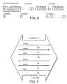
- the first byte of each message will be a header byte, the structure of which for each of the four messages is illustrated in Figure 6.
- the header byte constitutes a packet identifier to identify the nature of the packet.
- the first two bits of a header byte constitute a type identifier to identify the type of message, i.e. whether the message is a poke, a peek, a peeked, or an event message.
- the following six bits of the header byte act as a length indicator to identify the number of words following the header byte and associated with that message, thus indicating the length of the packet.
- four bits provide a reason indicator and two bits define a channel identifier (CI).
- Figure 7 illustrates the structure of each of four types of message according to the described embodiment.
- Figure 7a shows a poke message as comprising a poke header byte 00+WORDCCUNT, followed by an address word, and followed by at least one data word.
- Figure 7b shows a peek message as comprising a peek header byte 01+WORDCOUNT followed by an address word.
- Figure 7c shows a peeked message as comprising a peeked header byte 10+WORDCOUNT followed by at least one data word.
- Figure 7d shows an event message as comprising an event header byte only, 11+CI+REASON. The operation of the three memory access messages is discussed only briefly herein because they are described in more detail in our earlier Application EP-A-840218. The event message is discussed in the following.
- the two channel identifier bits CI identify the channel on which communication is to be established on-chip.
- the reason code identified by the remaining four bits applies to the indicated channel. Any event message, and all following non-event messages, if any, apply to the identified channel.
- the initial state is channel 0, so that an initial event message is not required and the default communication, in both directions, is channel 0.
- An event message which changes channels is allowed to occur between a peek and its corresponding peeked message, as illustrated for example in Figure 8 and described in more detail hereinafter.
- the byte counter 214 On receipt of a message on RXDATA 94 by the receive demultiplexor 208, the byte counter 214 is loaded with the number of bytes expected for each message computed from the word count extracted from the header of each message. The byte count is decremented as each byte within the message passes through. When the byte count is zero, then the next byte is a header.
- the event detector 212 looks at each byte and decodes the channel identifier.
- the receive state machine 220 observes the output from the byte counter 214 and the event detector 212 and determines from the channel identifier the channel (i.e. channel 0 or channel 1) for this and subsequent messages.
- the identified channel controls passage of the message either to the first receive buffer 216 or the second receive buffer 218 and connects the control signals 100,102 with the control signals of the appropriate channel.
- the channel identifier or channel number denotes channel 0
- the control signals 100,102 are connected to lines 228 and 222 respectively.
- the message is placed into the first receive buffer 216 and output via data path 230 for communication via channel 0.
- the transmit multiplexor passes the channel stream data from whichever channel is communicating to the transmit stream TXDATA 92 and connects together the corresponding control signals. It also inserts an event packet when the communicating channel changes. If both channels have data available for transmission, the messages from each are sent alternately.
- the byte counter 238 is loaded with the number of bytes expected for each message computed from the word count extracted from the header of each message.
- the byte counter is decremented as each byte within the message passes through.
- the transmit state machine 244 connects the control signals of the communicating channel with the transmit control signals 96,98.
- the transmit state machine 244 also determines when there is to be a change in communicating channel.
- the event generator 242 To effect that change, it switches over connection of the control signals to the control signals of the other channel (or another channel if there are more than two communicating channels) and triggers the event generator 242 to generate an event packet identifying the channel to which communication has just been switched. That event packet identifies the channel in the CI bits 6 and 7 in Figure 6(d), and identifies as a reason in bits 2 to 5 that there has been a channel change.
- the generated event packet is launched via the transmit data path 92 after all bytes of the message currently being conveyed on the first communicating channel have been conveyed. This is determined by the byte counter 238.
- Figure 10 illustrates in schematic form one arrangement which makes use of the multi-core data adaptor 202 to establish a connection between independent debugger hosts and independent on-chip processing cores.
- reference numerals 300 and 300' denotes independent host CPUs, each with their own communications port for transmitting messages via a communication channel 306 such as Ethernet.
- Reference numeral 308 denotes an off-chip adaptor circuit which includes the necessary circuitry for converting data received via the TAP controller 4 into messages in a format comprehensible by the host CPUs. Such circuitry is described in more detail in our earlier case EP-A-0840217.
- the adaptor circuit 308 generates the TAP controller signals 14,16,18 and 22 defined above with respect to Figure 1 and receives the output signal 20.
- the integrated circuit comprises two independent processing cores 310,310'.
- Each processing core comprises a message converter 160,160', diagnostic facilities 163,163', a target CPU 162,162', and on-chip memory 164,164'. These blocks are all interconnected by a bus system (shown dotted) which can communicate with the respective channel in communication with the particular processing core.
- the bus system for each processing core can be connected to off-chip memory 174,174' by an off-chip connection 316,316' respectively.
- the message converter operates to decode and encode messages for transmission from and to the communication channel, for off-chip communication and for the processing core. Its operation is described in more detail in our earlier application EP-A-0840218 (PWF Ref. 85515).
- the diagnostics facilities 163 can include diagnostic registers which can be read to or written from via a diagnostic bus 312. Control information associated with the target CPU 162 (or 162') is read from the diagnostic facilities 300.
- the instruction pointer and other control signals associated with each target CPU are stored in the diagnostic registers of the respective diagnostic facilities. The instruction pointer is continually copied into one of the diagnostic registers and can be accessed by a request on the diagnostic bus.
- the diagnostic registers can store various control signals of the target CPU, for example, STORE, TRAP, TAKEATRAP, TRAPATNEXTEXIT.
- each host CPU may write to registers within the diagnostic facilities via the diagnostic bus 312 (or 312').
- Each host CPU 300,300' can communication independently with each processing core 310,310' via the respective channels 206,204. For each case, in response to the host CPU writing to the registers of the diagnostic facilities, triggered events may occur. Such triggered events are detected in the message converter which generates a suitable header byte to transmit an event message off-chip.
- the target CPU can itself access the diagnostic facilities and in doing so this may cause a triggered event to occur which is translated into a message at the message converter 160 (or 160') and is returned on the appropriate channel to the multi-core date adaptor 202.
- the multi-core data adaptor ensures that the message is transmitted off-chip and reaches the appropriate host CPU by virtue of the channel identifier.
- Figure 10 allows independent debugging operations to be carried out between each host CPU 300 and 300' and a respective independent processing core 310,310' by virtue of the independent communication channels 206,204.
- FIG 11 illustrates another environment in which the multi-core data adaptor 202 can be used.
- the on-chip facilities are as already described with reference to Figure 10, as is the off-chip communications adaptor 308.
- the host CPU comprises an operating system 400 capable of running two independent debugger applications 402,402' for debugging respectively the independent processing cores 310,310' on-chip.
- channel 0, 206 can be defined to allow communication between the debugger application 402 and the on-chip processing core 310
- channel 1, 204 can be defined to allow communication between the debugger application 402' and the processing core 310'.
- FIG 12 illustrates yet another environment in which the multi-core data adaptor 202 can be used.
- On-chip facilities are as described with reference to Figure 10, as is the off-chip communications adaptor 308.
- the CPU has an operating system 400 which interfaces with a debugger application 404 with respective interface modules 406,406'.
- the communication channels 206,204 allow respective independent communication between each interface module 406,406' and its respective on-chip processing core 310,310'.
Landscapes
- Engineering & Computer Science (AREA)
- General Engineering & Computer Science (AREA)
- Theoretical Computer Science (AREA)
- Computer Hardware Design (AREA)
- Quality & Reliability (AREA)
- Physics & Mathematics (AREA)
- General Physics & Mathematics (AREA)
- Test And Diagnosis Of Digital Computers (AREA)
- Tests Of Electronic Circuits (AREA)
Claims (15)
- Integrierte Schaltung (2) umfassend:dadurch gekennzeichnet, dass die Datenanpassungseinheit umfasst:a) einen Eingangsanschluss (TDI) für serielle Daten und einen Ausgangsanschluss (TDO) für serielle Daten;b) einen funktionellen On-Chip-Schaltkreis mit mindestens zwei Verarbeitungskernen (310, 310');c) eine Datenanpassungseinheit (202), die mit den Verarbeitungskernen durch jeweilige Kommunikationskanäle verbunden ist und angeordnet ist, um mit dem Eingangsanschluss und dem Ausgangsanschluss verbunden zu werden,i) einen Sendeschaltkreis (210) mit einer Empfangseinrichtung (238, 244) zum Empfangen von ersten parallelen Daten und Steuersignalen von dem funktionellen On-Chip-Schaltkreis, undii) eine Konvertierungseinrichtung (242) zum Konvertieren der ersten parallelen Daten und der Steuersignale in eine ersten Abfolge von seriellen Bits, die Flusssteuerbits, Datenbits und Kanalidentifikationsbits, die den Kommunikationskanal (0,1) identifizieren, auf dem parallele Daten und Steuersignale empfangen werden, enthalten, undiii) einen Empfangsschaltkreis (208) mit einer Empfangseinrichtung (214, 220) zum Empfangen einer zweiten Abfolge von seriellen Bits, die Flusssteuerbits, Datenbits und Kanalidentifikationsbits enthalten, von außerhalb des Chips über den Eingangsanschluss für serielle Daten;iv) eine Konvertierungseinrichtung (212) zum Konvertieren der zweiten Abfolge in zweite parallele Daten und Steuersignale für den funktionellen On-Chip-Schaltkreis; undv) eine Sendeeinrichtung (216, 218) zum Senden der zweiten parallelen Daten und Steuersignale auf dem Kommunikationskanal (0,1), der durch die Kanalidentifikationsbits identifiziert ist.
- Integrierte Schaltung nach Anspruch 1, wobei die Konvertierungseinrichtung in dem Empfangsschaltkreis (208) eine Decodiereinrichtung (212) zum Decodieren einer Ereignisabfolge von seriellen Bits umfasst, wobei die Ereignisabfolge Kanalidentifikationsbits enthält.
- Integrierte Schaltung nach Anspruch 1 oder 2, wobei die Konvertierungseinrichtung in dem Sendeschaltkreis einen Ereignisgenerator (242) umfasst, der eine Ereignisabfolge von Bits erzeugt, um den Kommunikationskanal (0,1), auf dem Daten übertragen werden, zu identifizieren.
- Integrierte Schaltung nach Anspruch 3, wobei der Ereignisgenerator (242) geeignet ist, nur dann eine Ereignisabfolge zu erzeugen, wenn der momentane Kommunikationskanal (0,1) auf einen alternativen Kommunikationskanal geschaltet ist.
- Integrierte Schaltung gemäß einem der vorangehenden Ansprüche, wobei jeder Verarbeitungskern (310, 310') mindestens einen autonomen operierenden Prozessor (162, 162') umfasst.
- Integrierte Schaltung gemäß einem der vorangehenden Ansprüche, wobei jeder Verarbeitungskern (310, 310') einen Nachrichtenkonvertierer (160, 160') aufweist, der Nachrichten, die aus dem Chip über die Datenanpassungseinheit (202) gesendet werden sollen, zusammenstellt und Nachrichten, die On-Chip über die Datenanpassungseinheit empfangen werden, decodiert.
- Integrierte Schaltung gemäß einem der vorangehenden Ansprüche, wobei jeder Verarbeitungskern (310, 310') einen On-Chip-Speicher (164, 164') enthält.
- Integrierte Schaltung gemäß einem der vorangehenden Ansprüche, wobei jeder Verarbeitungskern (310, 310') ein Bussystem (204, 206) zum Kommunizieren mit einem chipexternen Speicher umfasst.
- Integrierte Schaltung gemäß einem der vorangehenden Ansprüche, wobei jeder Verarbeitungskern (310, 310') eine Anzahl von Registern (163, 163') umfasst, die Informationen zu Diagnosezwecken speichern, wobei die Register von außerhalb des Chips über die Datenanpassungseinheit (202) und den Kommunikationskanal (0,1), der dem jeweiligen Verarbeitungskern zugeordnet ist, zugreifbar sind.
- Integrierte Schaltung gemäß einem der vorangehenden Ansprüche, die weiterhin eine Steuereinheit(4) für eine Testzugangsschnittstelle umfasst, die so geschaltet ist, um die Kommunikation der seriellen Daten über die Chipgrenzen hinaus über den Eingangsanschluss (TDI) und Ausgangsanschluss (TDO) steuert, wobei die Steuereinheit(4) für die Testzugangsschnittstelle mit einer On-Chip-Testlogik (163, 163') in einem ersten Betriebsmodus und mit der Datenanpassungseinheit (202) in einem zweiten Betriebsmodus verbindbar ist.
- Computersystem umfassend:eine integrierte Schaltung (2) mit einem einzigen Chip gemäß einem der vorangehenden Ansprüche;mindestens zwei unabhängig operierende außerhalb des Chips angeordnete Prozessoren (162, 162'); undeine außerhalb des Chips angeordnete Host-Kommunikationsanpassungseinheit (308), die mit den externen Prozessoren verbunden ist und ausgestaltet ist, um parallele Daten und Steuersignale von den außerhalb des Chip angeordneten Prozessoren in einer Abfolge von seriellen Bits für die On-Chip-Kommunikation zu konvertieren.
- Computersystem umfassend:eine integrierte Schaltung (2) auf einem einzelnen Chip gemäß einem der Ansprüche 1 bis 10;ein außerhalb des Chip angeordneter Hostprozessor (300), der geeignet ist, unabhängig mindestens zwei Fehleranalyseanwendungen (402, 402') zu betreiben; undeine außerhalb des Chips angeordnete Host-Kommunikationsanpassungseinheit (308), die so geschaltet ist, um Nachrichten von dem Hostprozessor zu empfangen und die Nachrichten von einer Form aus parallelen Daten und Steuersignalen in einer Abfolge von seriellen Bits für die On-Chip-Kommunikation zu konvertieren.
- Computersystem umfassend:eine integrierte Schaltung (2) auf einem einzelnen Chip gemäß einem der Ansprüche 1 bis 10, umfassend:ein außerhalb des Chips angeordneter Hostprozessor (300), der geeignet ist, eine Fehleranalyseanwendung (404) mit unabhängig betreibbaren Schnittstellenmodulen (406, 406') zu betreiben; undeine Hostkommunikationsanpassungseinheit (308), die mit dem Hostprozessor verbunden ist und die geeignet ist, Nachrichten, die in einer Form von parallelen Daten und Steuersignalen vorliegen, in eine Abfolge von seriellen Bits für die On-Chip-Kommunikation zu konvertieren.
- Verfahren zum Betreiben der Kommunikation von Nachrichten von einem oder mehreren unabhängigen Verarbeitungskernen (310, 310') auf einer integrierten Schaltung (2) zu einem außerhalb des Chips angeordneten Hostprozessor (300), wobei:a) einer der unabhängigen Verarbeitungskerne (310, 310') eine Nachricht zusammenstellt, die einen Nachrichtenidentifizierer, der die Art der Nachricht angibt, und einen Kanalidentifizierer enthält, der den Kommunikationskanal (0,1) angibt, über den der unabhängige Verarbeitungskern versucht, die Nachricht zu senden;b) die Nachricht über den identifizierten Kommunikationskanal an eine Datenanpassungseinheit (202) gesendet wird, die die Nachricht an ein geeignetes Format für die chipexterne Kommunikation anpasst;c) wenn ein alternativer unabhängiger Verarbeitungskern (310, 310') versucht, eine Nachricht zu kommunizieren, ein neuer Kommunikationskanal (0,1) für den alternativen unabhängigen Verarbeitungskern identifiziert wird und eine Ereignisnachricht zum Senden nach außerhalb des Chips erzeugt, die den alternativen Kommunikationskanal identifiziert.
- Verfahren nach Anspruch 14, wobei, wenn eine Nachricht innerhalb des Chips empfangen wird, der Kanalidentifizierer decodiert wird und die Nachricht an den Kommunikationskanal (0,1) versendet wird, der durch den Kanalidentifizierer identifiziert wird, so dass die Nachricht an einen Richtigen der unabhängigen Verarbeitungskerne (310,310') gesendet wird.
Applications Claiming Priority (2)
| Application Number | Priority Date | Filing Date | Title |
|---|---|---|---|
| GB9818377 | 1998-08-21 | ||
| GBGB9818377.5A GB9818377D0 (en) | 1998-08-21 | 1998-08-21 | An integrated circuit with multiple processing cores |
Publications (2)
| Publication Number | Publication Date |
|---|---|
| EP0982595A1 EP0982595A1 (de) | 2000-03-01 |
| EP0982595B1 true EP0982595B1 (de) | 2005-01-12 |
Family
ID=10837704
Family Applications (1)
| Application Number | Title | Priority Date | Filing Date |
|---|---|---|---|
| EP99306192A Expired - Lifetime EP0982595B1 (de) | 1998-08-21 | 1999-08-04 | Integrierte Schaltung mit mehreren Prozessorkernen |
Country Status (4)
| Country | Link |
|---|---|
| US (1) | US6675284B1 (de) |
| EP (1) | EP0982595B1 (de) |
| DE (1) | DE69923126D1 (de) |
| GB (1) | GB9818377D0 (de) |
Families Citing this family (81)
| Publication number | Priority date | Publication date | Assignee | Title |
|---|---|---|---|---|
| US6711620B1 (en) * | 1999-04-14 | 2004-03-23 | Matsushita Electric Industrial Co. | Event control device and digital broadcasting system |
| US6550020B1 (en) * | 2000-01-10 | 2003-04-15 | International Business Machines Corporation | Method and system for dynamically configuring a central processing unit with multiple processing cores |
| US6950963B1 (en) * | 2000-05-30 | 2005-09-27 | Agere Systems Inc. | Control method and apparatus for testing of multiple processor integrated circuits and other digital systems |
| US7139947B2 (en) * | 2000-12-22 | 2006-11-21 | Intel Corporation | Test access port |
| US7624204B2 (en) * | 2001-03-22 | 2009-11-24 | Nvidia Corporation | Input/output controller node in an adaptable computing environment |
| US6836839B2 (en) | 2001-03-22 | 2004-12-28 | Quicksilver Technology, Inc. | Adaptive integrated circuitry with heterogeneous and reconfigurable matrices of diverse and adaptive computational units having fixed, application specific computational elements |
| US7400668B2 (en) * | 2001-03-22 | 2008-07-15 | Qst Holdings, Llc | Method and system for implementing a system acquisition function for use with a communication device |
| US7962716B2 (en) | 2001-03-22 | 2011-06-14 | Qst Holdings, Inc. | Adaptive integrated circuitry with heterogeneous and reconfigurable matrices of diverse and adaptive computational units having fixed, application specific computational elements |
| US7752419B1 (en) | 2001-03-22 | 2010-07-06 | Qst Holdings, Llc | Method and system for managing hardware resources to implement system functions using an adaptive computing architecture |
| US7433909B2 (en) | 2002-06-25 | 2008-10-07 | Nvidia Corporation | Processing architecture for a reconfigurable arithmetic node |
| DE10119266A1 (de) * | 2001-04-20 | 2002-10-31 | Infineon Technologies Ag | Programmgesteuerte Einheit |
| US6577678B2 (en) | 2001-05-08 | 2003-06-10 | Quicksilver Technology | Method and system for reconfigurable channel coding |
| SG167663A1 (en) * | 2001-08-31 | 2011-01-28 | Adaptive Networks Inc | Communicating data using wideband communications |
| US20050091376A1 (en) * | 2001-10-12 | 2005-04-28 | Helfman Nadav B. | Apparatus and method for optimized and secured reflection of network services to remote locations |
| US8412915B2 (en) * | 2001-11-30 | 2013-04-02 | Altera Corporation | Apparatus, system and method for configuration of adaptive integrated circuitry having heterogeneous computational elements |
| US6986021B2 (en) | 2001-11-30 | 2006-01-10 | Quick Silver Technology, Inc. | Apparatus, method, system and executable module for configuration and operation of adaptive integrated circuitry having fixed, application specific computational elements |
| US7602740B2 (en) * | 2001-12-10 | 2009-10-13 | Qst Holdings, Inc. | System for adapting device standards after manufacture |
| US7088825B2 (en) * | 2001-12-12 | 2006-08-08 | Quicksilver Technology, Inc. | Low I/O bandwidth method and system for implementing detection and identification of scrambling codes |
| US20030108012A1 (en) * | 2001-12-12 | 2003-06-12 | Quicksilver Technology, Inc. | Method and system for detecting and identifying scrambling codes |
| US7215701B2 (en) | 2001-12-12 | 2007-05-08 | Sharad Sambhwani | Low I/O bandwidth method and system for implementing detection and identification of scrambling codes |
| US7231508B2 (en) * | 2001-12-13 | 2007-06-12 | Quicksilver Technologies | Configurable finite state machine for operation of microinstruction providing execution enable control value |
| US7403981B2 (en) * | 2002-01-04 | 2008-07-22 | Quicksilver Technology, Inc. | Apparatus and method for adaptive multimedia reception and transmission in communication environments |
| US7328414B1 (en) * | 2003-05-13 | 2008-02-05 | Qst Holdings, Llc | Method and system for creating and programming an adaptive computing engine |
| US7660984B1 (en) | 2003-05-13 | 2010-02-09 | Quicksilver Technology | Method and system for achieving individualized protected space in an operating system |
| US8108656B2 (en) | 2002-08-29 | 2012-01-31 | Qst Holdings, Llc | Task definition for specifying resource requirements |
| US7010722B2 (en) * | 2002-09-27 | 2006-03-07 | Texas Instruments Incorporated | Embedded symmetric multiprocessor system debug |
| US7937591B1 (en) | 2002-10-25 | 2011-05-03 | Qst Holdings, Llc | Method and system for providing a device which can be adapted on an ongoing basis |
| US8276135B2 (en) * | 2002-11-07 | 2012-09-25 | Qst Holdings Llc | Profiling of software and circuit designs utilizing data operation analyses |
| JP2004164367A (ja) * | 2002-11-14 | 2004-06-10 | Renesas Technology Corp | マルチプロセッサシステム |
| US7225301B2 (en) | 2002-11-22 | 2007-05-29 | Quicksilver Technologies | External memory controller node |
| US7787497B1 (en) * | 2003-03-03 | 2010-08-31 | Cisco Technology, Inc. | System for grouping attributes in packets in a radius protocol |
| US7103320B2 (en) * | 2003-04-19 | 2006-09-05 | International Business Machines Corporation | Wireless communication system within a system on a chip |
| US20050025120A1 (en) * | 2003-06-18 | 2005-02-03 | O'toole Anthony J.P. | Event scheduling for multi-port xDSL transceivers |
| US7609297B2 (en) * | 2003-06-25 | 2009-10-27 | Qst Holdings, Inc. | Configurable hardware based digital imaging apparatus |
| EP1544633B1 (de) | 2003-12-17 | 2008-10-01 | STMicroelectronics (Research & Development) Limited | TAP Multiplexer |
| DE602004026401D1 (de) * | 2004-02-24 | 2010-05-20 | Accent S P A | Verfahren zur Implementierung eines Abtastratenumsetzers mit rationalem Umsetzungsfaktor (FSRC) und entsprechende Architektur |
| US7698552B2 (en) | 2004-06-03 | 2010-04-13 | Intel Corporation | Launching a secure kernel in a multiprocessor system |
| US7941585B2 (en) * | 2004-09-10 | 2011-05-10 | Cavium Networks, Inc. | Local scratchpad and data caching system |
| US7809987B2 (en) * | 2004-12-02 | 2010-10-05 | Texas Instruments Incorporated | Accepting link ID upon supplied and sampled bits matching |
| US7552360B2 (en) | 2005-03-21 | 2009-06-23 | Texas Instruments Incorporated | Debug and test system with format select register circuitry |
| US7209066B1 (en) | 2005-10-18 | 2007-04-24 | Honeywell International Inc. | Circuit and method for extending microcontroller analog input capability |
| JP4450787B2 (ja) * | 2005-11-28 | 2010-04-14 | 株式会社ルネサステクノロジ | 半導体集積回路装置 |
| JP4277030B2 (ja) * | 2006-06-30 | 2009-06-10 | 株式会社日立製作所 | 通信制御システム |
| US7558987B2 (en) * | 2006-08-29 | 2009-07-07 | Texas Instruments Incorporated | Token-based trace system |
| US20080182021A1 (en) * | 2007-01-31 | 2008-07-31 | Simka Harsono S | Continuous ultra-thin copper film formed using a low thermal budget |
| US20090109996A1 (en) * | 2007-10-29 | 2009-04-30 | Hoover Russell D | Network on Chip |
| US20090125706A1 (en) * | 2007-11-08 | 2009-05-14 | Hoover Russell D | Software Pipelining on a Network on Chip |
| US20090125703A1 (en) * | 2007-11-09 | 2009-05-14 | Mejdrich Eric O | Context Switching on a Network On Chip |
| US8261025B2 (en) | 2007-11-12 | 2012-09-04 | International Business Machines Corporation | Software pipelining on a network on chip |
| US8032772B2 (en) | 2007-11-15 | 2011-10-04 | Intel Corporation | Method, apparatus, and system for optimizing frequency and performance in a multi-die microprocessor |
| WO2009065313A1 (fr) * | 2007-11-20 | 2009-05-28 | Hangzhou H3C Technologies Co., Ltd. | Procédé et équipement à processeur multicœurs pour la mise en œuvre de plusieurs fonctions de traitement de services |
| CN101442513B (zh) * | 2007-11-20 | 2012-05-23 | 杭州华三通信技术有限公司 | 实现多种业务处理功能的方法和多核处理器设备 |
| US8526422B2 (en) * | 2007-11-27 | 2013-09-03 | International Business Machines Corporation | Network on chip with partitions |
| US8473667B2 (en) * | 2008-01-11 | 2013-06-25 | International Business Machines Corporation | Network on chip that maintains cache coherency with invalidation messages |
| US8010750B2 (en) * | 2008-01-17 | 2011-08-30 | International Business Machines Corporation | Network on chip that maintains cache coherency with invalidate commands |
| US8103924B2 (en) * | 2008-01-29 | 2012-01-24 | Globalfoundries Inc. | Test access mechanism for multi-core processor or other integrated circuit |
| US8018466B2 (en) * | 2008-02-12 | 2011-09-13 | International Business Machines Corporation | Graphics rendering on a network on chip |
| US7913010B2 (en) * | 2008-02-15 | 2011-03-22 | International Business Machines Corporation | Network on chip with a low latency, high bandwidth application messaging interconnect |
| US8490110B2 (en) * | 2008-02-15 | 2013-07-16 | International Business Machines Corporation | Network on chip with a low latency, high bandwidth application messaging interconnect |
| US20090245257A1 (en) * | 2008-04-01 | 2009-10-01 | International Business Machines Corporation | Network On Chip |
| US20090260013A1 (en) * | 2008-04-14 | 2009-10-15 | International Business Machines Corporation | Computer Processors With Plural, Pipelined Hardware Threads Of Execution |
| US20090271172A1 (en) * | 2008-04-24 | 2009-10-29 | International Business Machines Corporation | Emulating A Computer Run Time Environment |
| US8078850B2 (en) * | 2008-04-24 | 2011-12-13 | International Business Machines Corporation | Branch prediction technique using instruction for resetting result table pointer |
| US8423715B2 (en) * | 2008-05-01 | 2013-04-16 | International Business Machines Corporation | Memory management among levels of cache in a memory hierarchy |
| US7991978B2 (en) | 2008-05-09 | 2011-08-02 | International Business Machines Corporation | Network on chip with low latency, high bandwidth application messaging interconnects that abstract hardware inter-thread data communications into an architected state of a processor |
| US8494833B2 (en) * | 2008-05-09 | 2013-07-23 | International Business Machines Corporation | Emulating a computer run time environment |
| US8020168B2 (en) * | 2008-05-09 | 2011-09-13 | International Business Machines Corporation | Dynamic virtual software pipelining on a network on chip |
| US20090282419A1 (en) * | 2008-05-09 | 2009-11-12 | International Business Machines Corporation | Ordered And Unordered Network-Addressed Message Control With Embedded DMA Commands For A Network On Chip |
| US20090282211A1 (en) * | 2008-05-09 | 2009-11-12 | International Business Machines | Network On Chip With Partitions |
| US8392664B2 (en) * | 2008-05-09 | 2013-03-05 | International Business Machines Corporation | Network on chip |
| US8214845B2 (en) | 2008-05-09 | 2012-07-03 | International Business Machines Corporation | Context switching in a network on chip by thread saving and restoring pointers to memory arrays containing valid message data |
| US7958340B2 (en) | 2008-05-09 | 2011-06-07 | International Business Machines Corporation | Monitoring software pipeline performance on a network on chip |
| US8230179B2 (en) * | 2008-05-15 | 2012-07-24 | International Business Machines Corporation | Administering non-cacheable memory load instructions |
| US8040799B2 (en) * | 2008-05-15 | 2011-10-18 | International Business Machines Corporation | Network on chip with minimum guaranteed bandwidth for virtual communications channels |
| US8438578B2 (en) * | 2008-06-09 | 2013-05-07 | International Business Machines Corporation | Network on chip with an I/O accelerator |
| US8195884B2 (en) * | 2008-09-18 | 2012-06-05 | International Business Machines Corporation | Network on chip with caching restrictions for pages of computer memory |
| US9262292B2 (en) * | 2012-06-11 | 2016-02-16 | New York University | Test access system, method and computer-accessible medium for chips with spare identical cores |
| US9330040B2 (en) * | 2013-09-12 | 2016-05-03 | Qualcomm Incorporated | Serial configuration of a reconfigurable instruction cell array |
| WO2015075505A1 (en) * | 2013-11-22 | 2015-05-28 | Freescale Semiconductor, Inc. | Apparatus and method for external access to core resources of a processor, semiconductor systems development tool comprising the apparatus, and computer program product and non-transitory computer-readable storage medium associated with the method |
| US10581554B2 (en) * | 2017-01-13 | 2020-03-03 | Dolby Laboratories Licensing Corporation | Systems and methods to generate copies of data for transmission over multiple communication channels |
| CN110134640B (zh) * | 2018-02-09 | 2024-03-01 | 上海中研久弋科技有限公司 | 多核心传感器数据处理芯片及运行方法 |
Family Cites Families (12)
| Publication number | Priority date | Publication date | Assignee | Title |
|---|---|---|---|---|
| EP0652516A1 (de) * | 1993-11-03 | 1995-05-10 | Advanced Micro Devices, Inc. | Integrierter Mikroprozessor |
| US5535222A (en) * | 1993-12-23 | 1996-07-09 | At&T Corp. | Method and apparatus for controlling a plurality of systems via a boundary-scan port during testing |
| US5533192A (en) * | 1994-04-21 | 1996-07-02 | Apple Computer, Inc. | Computer program debugging system and method |
| JP2752592B2 (ja) * | 1994-12-28 | 1998-05-18 | 日本ヒューレット・パッカード株式会社 | マイクロプロセッサ、マイクロプロセッサ−デバッグツール間信号伝送方法及びトレース方法 |
| US5732209A (en) * | 1995-11-29 | 1998-03-24 | Exponential Technology, Inc. | Self-testing multi-processor die with internal compare points |
| GB9622682D0 (en) * | 1996-10-31 | 1997-01-08 | Sgs Thomson Microelectronics | An integrated circuit device and method of communication therewith |
| EP0840221B1 (de) * | 1996-10-31 | 2002-09-18 | STMicroelectronics Limited | Mikrorechner mit Paketbus |
| GB9622687D0 (en) * | 1996-10-31 | 1997-01-08 | Sgs Thomson Microelectronics | An integrated circuit with tap controller |
| GB9622684D0 (en) * | 1996-10-31 | 1997-01-08 | Sgs Thomson Microelectronics | An integrated circuit device and method of communication therwith |
| JPH1139190A (ja) * | 1997-07-22 | 1999-02-12 | Fujitsu Ltd | 並列処理プログラムのデバッグシステム、及びそのデバッグ方法 |
| US6516442B1 (en) * | 1997-12-07 | 2003-02-04 | Conexant Systems, Inc. | Channel interface and protocols for cache coherency in a scalable symmetric multiprocessor system |
| US6134675A (en) * | 1998-01-14 | 2000-10-17 | Motorola Inc. | Method of testing multi-core processors and multi-core processor testing device |
-
1998
- 1998-08-21 GB GBGB9818377.5A patent/GB9818377D0/en not_active Ceased
-
1999
- 1999-08-04 DE DE69923126T patent/DE69923126D1/de not_active Expired - Lifetime
- 1999-08-04 EP EP99306192A patent/EP0982595B1/de not_active Expired - Lifetime
- 1999-08-20 US US09/378,909 patent/US6675284B1/en not_active Expired - Lifetime
Also Published As
| Publication number | Publication date |
|---|---|
| DE69923126D1 (de) | 2005-02-17 |
| GB9818377D0 (en) | 1998-10-21 |
| EP0982595A1 (de) | 2000-03-01 |
| US6675284B1 (en) | 2004-01-06 |
Similar Documents
| Publication | Publication Date | Title |
|---|---|---|
| EP0982595B1 (de) | Integrierte Schaltung mit mehreren Prozessorkernen | |
| EP0840134B1 (de) | Nachrichtenübertragungsverfahren für eine Testzugriffsportsteuerungsvorrichtung (TAP) | |
| US5978870A (en) | On-chip parallel-serial data packet converter to interconnect parallel bus of integrated circuit chip with external device | |
| US6125416A (en) | Method and device for communicating across a chip boundary including a serial-parallel data packet converter having flow control logic | |
| EP0849670B1 (de) | Integrierter Rechner mit Befehlsverfolgung | |
| EP0840217B1 (de) | Eine integrierte Schaltung mit einer TAP (Testzugriffport) Steuerungsvorrichtung | |
| EP0849668B1 (de) | Diagnosesystem und Verfahren bei einer integrierten Halbleiterschaltung | |
| EP0849669B1 (de) | Diagnosesystem und Verfahren bei einer integrierten Schaltung | |
| EP0862115B1 (de) | Steuervorrichtung einer Auslösesignalreihenfolge | |
| EP0840218B1 (de) | Integrierte Halbleiterspeicheranordnung und Kommunikationsverfahren dafür | |
| EP0840235B1 (de) | Nachrichtenprotokoll | |
| US6526535B1 (en) | Synchronous data adaptor | |
| US6381721B1 (en) | Detecting communication errors across a chip boundary | |
| EP1293790A1 (de) | Abfrageprüfgerät des Überabtastung zur Synchronisierung verwendet |
Legal Events
| Date | Code | Title | Description |
|---|---|---|---|
| PUAI | Public reference made under article 153(3) epc to a published international application that has entered the european phase |
Free format text: ORIGINAL CODE: 0009012 |
|
| AK | Designated contracting states |
Kind code of ref document: A1 Designated state(s): DE FR GB IT |
|
| AX | Request for extension of the european patent |
Free format text: AL;LT;LV;MK;RO;SI |
|
| 17P | Request for examination filed |
Effective date: 20000726 |
|
| AKX | Designation fees paid |
Free format text: DE FR GB IT |
|
| 17Q | First examination report despatched |
Effective date: 20040325 |
|
| GRAP | Despatch of communication of intention to grant a patent |
Free format text: ORIGINAL CODE: EPIDOSNIGR1 |
|
| GRAS | Grant fee paid |
Free format text: ORIGINAL CODE: EPIDOSNIGR3 |
|
| GRAA | (expected) grant |
Free format text: ORIGINAL CODE: 0009210 |
|
| AK | Designated contracting states |
Kind code of ref document: B1 Designated state(s): DE FR GB IT |
|
| PG25 | Lapsed in a contracting state [announced via postgrant information from national office to epo] |
Ref country code: IT Free format text: LAPSE BECAUSE OF FAILURE TO SUBMIT A TRANSLATION OF THE DESCRIPTION OR TO PAY THE FEE WITHIN THE PRESCRIBED TIME-LIMIT;WARNING: LAPSES OF ITALIAN PATENTS WITH EFFECTIVE DATE BEFORE 2007 MAY HAVE OCCURRED AT ANY TIME BEFORE 2007. THE CORRECT EFFECTIVE DATE MAY BE DIFFERENT FROM THE ONE RECORDED. Effective date: 20050112 |
|
| REG | Reference to a national code |
Ref country code: GB Ref legal event code: FG4D |
|
| REF | Corresponds to: |
Ref document number: 69923126 Country of ref document: DE Date of ref document: 20050217 Kind code of ref document: P |
|
| PG25 | Lapsed in a contracting state [announced via postgrant information from national office to epo] |
Ref country code: DE Free format text: LAPSE BECAUSE OF FAILURE TO SUBMIT A TRANSLATION OF THE DESCRIPTION OR TO PAY THE FEE WITHIN THE PRESCRIBED TIME-LIMIT Effective date: 20050413 |
|
| PGFP | Annual fee paid to national office [announced via postgrant information from national office to epo] |
Ref country code: DE Payment date: 20050728 Year of fee payment: 7 |
|
| PLBE | No opposition filed within time limit |
Free format text: ORIGINAL CODE: 0009261 |
|
| STAA | Information on the status of an ep patent application or granted ep patent |
Free format text: STATUS: NO OPPOSITION FILED WITHIN TIME LIMIT |
|
| ET | Fr: translation filed | ||
| 26N | No opposition filed |
Effective date: 20051013 |
|
| PGFP | Annual fee paid to national office [announced via postgrant information from national office to epo] |
Ref country code: FR Payment date: 20070829 Year of fee payment: 9 |
|
| REG | Reference to a national code |
Ref country code: FR Ref legal event code: ST Effective date: 20090430 |
|
| PG25 | Lapsed in a contracting state [announced via postgrant information from national office to epo] |
Ref country code: FR Free format text: LAPSE BECAUSE OF NON-PAYMENT OF DUE FEES Effective date: 20080901 |
|
| PGFP | Annual fee paid to national office [announced via postgrant information from national office to epo] |
Ref country code: GB Payment date: 20180720 Year of fee payment: 20 |
|
| REG | Reference to a national code |
Ref country code: GB Ref legal event code: PE20 Expiry date: 20190803 |
|
| PG25 | Lapsed in a contracting state [announced via postgrant information from national office to epo] |
Ref country code: GB Free format text: LAPSE BECAUSE OF EXPIRATION OF PROTECTION Effective date: 20190803 |