EP0839354B1 - Speicherstruktur - Google Patents
Speicherstruktur Download PDFInfo
- Publication number
- EP0839354B1 EP0839354B1 EP96917795A EP96917795A EP0839354B1 EP 0839354 B1 EP0839354 B1 EP 0839354B1 EP 96917795 A EP96917795 A EP 96917795A EP 96917795 A EP96917795 A EP 96917795A EP 0839354 B1 EP0839354 B1 EP 0839354B1
- Authority
- EP
- European Patent Office
- Prior art keywords
- memory
- information
- input
- structure according
- control logic
- Prior art date
- Legal status (The legal status is an assumption and is not a legal conclusion. Google has not performed a legal analysis and makes no representation as to the accuracy of the status listed.)
- Expired - Lifetime
Links
Images


Classifications
-
- G—PHYSICS
- G06—COMPUTING; CALCULATING OR COUNTING
- G06F—ELECTRIC DIGITAL DATA PROCESSING
- G06F12/00—Accessing, addressing or allocating within memory systems or architectures
- G06F12/02—Addressing or allocation; Relocation
- G06F12/04—Addressing variable-length words or parts of words
Definitions
- the present invention relates to a memory structure of the type which is stated in the preamble of Claim 1.
- the size of the memory is always limited by the propagation speed of the signals.
- increased memory area implies increased access time because the complexity of the address decoder increases when the memory increases.
- the demand for data processing speed is constantly increasing. Since the complexity of the address decoder increases and the propagation speed is constant, then the total storage space, that is to say the addressable surface where information can be stored, always decreases with increased computer speed.
- US, A, 4 747 070 discloses a memory structure adapted for storing vectors.
- the disclosed memory structure provides for M parallel memory banks. Each memory bank is N words deep. M words may be read from the memory at a time.
- the parallel memory structure enables increased transfer rate between system memory and processor. Each memory bank is addressed separately.
- US, A, 4 858 107 discloses a memory structure, which allows the introduction of a priority scheme between a central processing unit and a video display processor.
- the memory is organized into banks or bit planes each with temporary storage latch that loads to a respective shift register.
- Each memory bank or bit plane is provided with a separate address.
- An object of the invention is to produce a memory structure which is adapted for storing vectors.
- Another object of the invention is to produce a memory structure which gives fast and continuous access to storage places for the reading and/or writing of vectors.
- a further object of the invention is to produce a structure where the writing of a vector can take place at the same time as, and independently of, the reading of a vector is taking place.
- Yet a further object of the invention is to produce a memory structure where the writing of a vector can take place almost simultaneously with the reading of it.
- Yet another object of the invention is to produce a memory structure where the time for outputting written data can be controlled right down to the clock period.
- Yet another object of the invention is to produce a memory structure which can be used as a complement to the current type of memory structure for a computer.
- a further object of the invention is to produce a memory structure which permits the treatment of a stored vector parallelly by a plurality of storage positions for vectors in order to either reposition the processed vector or to get out a processing result.
- each of the storage positions in the memory has a length adapted for the length of the large vectors and are arranged parallelly, extending from an information input and deeper into the memory so that each vector is arranged to be stored undivided in consecutive order with the beginning of the vector by the input of the memory, whereby addressing is arranged to take place to the input of the memory.
- the memory is preferably divided transversely into memory blocks, so that all storage positions each have a part in each memory block.
- the storage positions in the memory can be lengthenable through joining together of one or more memory blocks.
- Each memory block can comprise:
- a control logic is arranged in each memory block, which control logic controls the input of information in memory fields via the input buffer whereby the memory blocks are cascade coupled with each other through the input buffers in them being cascade coupled with each other, so that information is serially stepwise feedable through a number of the buffers in the different memory blocks after one another, and the control logic in each memory block is arranged to inform the control logic in the next memory block when the memory fields in its own memory block are filled with information or all information in them is read out, so that the control logic in the next memory block can take over the job of writing the information to this memory block.
- the memory structure according to the invention permits the setting up of a large and expandable storage space for information, continuous data transfer and at the same time extremely high transfer speeds. Expansion of the storage space for a vector, and thereby the size of the memory, can be performed without affecting the data transfer speed as the interface with the memory seen from outside is unchanged.
- a continuous data transfer can be performed at approximately 0.5-1 Gbytes/sec compared with todays 30-100 Mbytes/sec. This implies a factor of ten times faster with the use of corresponding basic technology.
- the memory structures in themselves are not dependent on the technology used but can be used for arbitrary storage technologies (RAM, magnetic memory, optical memory etc.).
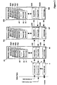
- Figure 1 shows a number of memory blocks #1, #2....#M. which are cascade coupled with each other.
- Each memory block has an information part 1I. 2I...MI. and input buffer 1IB respectively 2IB... respectively MIB, an output buffer 1UB respectively 2UB... respectively MUB and a control logic 1S respectively 2S ... respectively MS.
- Each memory block can be on a separate chip and a selected number of chips can be coupled together with each other in order to form an selectively large memory. It is also possible and appropriate to have several memory blocks on one chip whereby several multiblock chips can be coupled together in cascade.
- Each of the storage positions in the memory has a length adapted to the length of large vectors.
- the blocks are arranged in parallel extending from an in/output for information and deeper into the memory so that each vector is arranged to be stored undivided in consecutive order via the input buffers with the beginning of the vector at the input/output of the memory and similarly to be outputted in consecutive order via the output buffers when the need for this occurs (see the embodiment in Figure 7). Addressing is made to the in/output of the memory.
- the memory structure comprises a number of cascade coupled units or memory blocks #1 - #M. control logic 4 and where appropriate converter units 5, 6.
- the memory blocks shown here have each a constituant block with several memory planes #11 - #1N respectively "M1 - #MN lying behind one another which each comprise a number of memory fields F1 - FP.
- a special memory field in the memory has a reference which identifies which memory block and which memory plane it belongs to, for example #m, Qi, Fj for a memory field Fj in the memory plane Qi in the memory block #m. This reference system has been applied throughout.
- the memory blocks in practice can have a surface structure with the planes arranged spread-out at different positions on the surface or arranged as memory fields one after another, so that for example in the case of a chip with several blocks the memory fields in memory blocks #2/memory plane #Q1 are arranged as a direct continuation of the memory fields in the memory block #1/memory plane #Q1 etc.
- Each memory block #m has a number of memory fields F1 to FP allocated to each addressable memory plane Qi.
- Each memory block #m is physically organised in W m rows (corresponding to NxP in Figure 3) and axb columns. Each row forms a memory field and contains a number of byte groups or words (a) each with a suitable number of bits (b).
- the memory block #m is therefore W m x a x b bits large.
- the memory structure has a total size of (W 1 +W 2 + ... +W M ) x a x b bits. It is also possible to conceive the special case where a, b and W vary between memory blocks but this is not taken up here.
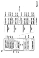
- a vector Vi with the length L i words is stored as L i /a partial vectors in memory fields M1, F1, ..., M1, FP; M2 F1, ..., M2 FP; ..., MN F1, ..., MN FP.
- the size of vector Vi is consequently a x b x(O i1 +O i2 + ... +O iM ) bits.
- W m O 1m + O 2m + ... +O Nm .
- Vectors of varying lengths can be stored at the same time in the memory structure.
- the memory structure can be configured in various ways. Seen from outside the vectors are addressed only from the starting point (the identity) #1 Mi F1 where i is any number between 1 and N, and F1 is the first memory field in the memory block #1 in the memory plane Mi.
- the length of the vectors L i is defined by the configuration.
- the configuration can be static or dynamic.
- the control logic 4 has knowledge of the number N of storage positions Mi as well as the length of the respective storage positions L i .
- the control logic 1S - MS in the memory blocks has knowledge of starting point #1 Qi F1 and the length O im for the respective memory block.
- the end point #m Qi Fj is defined indirectly by the starting point and length.
- the length of the current memory plane or storage position Mi is changed during writing.
- the information vector is assumed from outside to be followed by information on the length as well as other global information. This information can alternatively be found in the first byte group as a head of the vector Vi.
- the control logic can then read, use and change this information in accordance to how it extends further into the memory structure. After the head the information follows sequentially.
- Every memory block #i has an input buffer iIB with a buffer store comprising a number of storage bits for each storage memory field in the memory plane for incoming information and an output buffer iUB with the same buffer storage size as the input buffer for outputting information.
- the computer unit which via interface 5, 6 (see Figure 2) is connected to the memory structure according to the invention loads incoming information through the information inport and takes out outputted information from the information outport in the form of vectors, for example data packets.
- Each vector can be equipped with a head containing identity, length etc. Alternatively the necessary information can be given to the interface by any other way which is obvious for the man skilled in the art.
- a control logic 4 is coupled to the interface in order to control the memory in accordance with what has been read from it.
- the control logic 4 can furthermore be equipped with an internal memory (not shown) for storing data concerning the stored vectors and where these are stored in the memory and where new vectors can be stored.
- an internal memory not shown
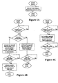
- Figures 4A-4C show a flow diagram of an embodiment of the way of the control logic works, partly during activation (Figure 4A), partly during writing into the memory ( Figure 4B) and partly during reading from the memory ( Figure 4C).
- the flow diagrams are so clear that a close description of the different stages does not need to be made.
- the inputted information to the memory is suitably of parallel type, that is to say in the form of parallel bytes of suitable length, for example 8, 16, 32 bits. If pure serial information is inputted then a conversion from the bit form to parallel byte form takes place in the converter unit 5. Similarly a conversion from parallel bytes to bits should be performed in the converter unit 6 if this is necessary. It should be noticed that there is nothing which prevents that the input information in the information inport being in serial bit form and the information in the information outport being in parallel byte form or vice versa in which case only one convener unit 5 or 6 is necessary.
- every stored vector will have its beginning in memory field F1 in one of the planes Qi in memory block #1 and to extend from there deeper in to the memory.
- Many of the memory fields F1 - FP will actually be used in each memory block for storage so that the storage can be considered as being folded but in practice in fact the whole vector will lie arranged in an unbroken sequence from beginning to end from memory block to memory block.
- Every control logic in the memory blocks has inside it a memory with information on which memory planes and which memory fields in them are empty or are already filled.
- a search is first made either in control logic 4 or in control logic 1S to find an available storage plane.
- the input buffer is filled in a manner analogous with a shift register but output to the memory fields can take place either serially or parallelly, and preferably parallelly so that the whole of the memory content of the input buffer is emptied.
- control logix 1S has in this connection an input-field pointer (not shown) which gives the memory field which is current for writing.
- the input buffer 1IB is controlled to begin filling input buffer 2IB, in analogy with a shift register, serially, that is to say parallel byte after parallel byte until this is filled.
- the whole of the serial length of the shift register used as the buffer will be called from now on a serial byte, because it represents the number of clock signals, which is necessary in order to fill the buffer that is to say it represents the serial length of a parallel byte group.
- the input buffer When the input buffer is filled, it fills in the first memory field F1 in plane #2 Qx and the different following memory fields there are then filled in in the same way as the memory field in memory plane #1 Qx, i.e. controlled by the input-field pointer from the control logic.
- the memory plane #1 Qx When the memory plane #1 Qx is filled, information in the input buffer 2IB of memory block #2 continues to be transferred over to the input buffer of the next memory block and subsequently from this to the memory fields in the next memory plane #3 Qx in this memory block and so on. It should be noted that it is possible to have many input and output buffers, for example in order to serve several memory planes simultaneously, even if this is not shown in any of the figures.
- the control unit can also be duplicated.
- each buffer in fact comprises as many parallel shift registers as there are bits in each byte.
- the expression parallel byte group is used for the number of bytes which fill an input/output buffer.
- Data can be read and outputted from a memory field immediately after it has been written in.
- control logic 1S activates control logic 2s to transfer the contents in the first memory field #2 Qi to the output buffer 2UB.
- an output buffer 2UB outputs its contents parallel byte after parallel byte serially to the output buffer 1UB so that this follows directly after the earlier contents of buffer 1UB.
- each output buffer in the different blocks serially outputs its contents, a parallel byte group, parallel byte after parallel byte to the next output buffer.
- Each parallel byte group can contain a relatively large number of parallel bytes in this case which means that the start of the output of a vector with data can take place with the relatively long time interval of a number of clock periods which is given by the length of the parallel byte group.
- the head logic of the memory has information about in which parallel byte group the output shall take place and also the phase displacement which is needed within the time length of the parallel byte group for the outputting to take place at the exact desired time.
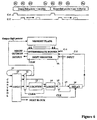
- FIG. 6 An embodiment of the memory with a control logic to achieve this is shown in Figure 6. It is possible to have outputting of the same memory contents to different parts of the system at independently controllable time points and in that case it is possible to have many output buffers coupled to the memory planes. However, in the figures only one output buffer OUTBUFF is shown. Each output buffer comprises an intermediate buffer MBUFF in which during controlling the contents are transferable to shift register sk. The way of functioning for each output buffer is course similar whereby the description concerning OUTBUFF is valid for all of them.
- the local control arrangement in a memory block receives an indication that the memory contents in a memory plane are to be outputted via an output buffer OUTBUFF
- the first memory field in this memory plane is loaded down in intermediate buffer MBUFF by means of a control signal C-1 for it.
- the appropriate clock signal for the actual outputting the contents of the intermediate buffer is transferred by means of a control signal C-2 to the shift register sk for the timed outputting directly with controlling on the clock input CLK of the shift register.
- the contents in the next memory field is transferred to the intermediate buffer OUTBUFF either directly after the transfer from the intermediate buffer to the shift register or, preferably, at the beginning of the next whole parallel byte group period. There is, however, nothing which prevents the transfer to the intermediate buffer taking place any time during the interval before the transfer to the shift register sk, for example during the clock period directly before the transfer from the intermediate memory to the shift register.
- control means for the first output buffer OUTBUFF for the memory block for outputting the respective transfers from the respective memory fields in the memory plane to the intermediate buffer MBUFF and then from the memory buffer to the shift register sk is shown at the bottom of Figure 6.
- the output field pointer moves to the next memory field at the next control signal CLK/b and to the next with the next control signal etc. This is illustrated by the oval 13. Furthermore the phase displacement with respect to the phase for the output field pointer is illustrated in the upper part of the figure for the different positions PI - Pa, where a is the position length of a memory field, in the different fields Fi and F(i+1) whereby C-1 in this embodiment comes at the beginning of the output field pointer and C-2 is controllably displaced to the desired position, for example P2.
- the output from the counter 12 together with an output from the logic 11 are inputted to a second logic 14 concerning the change of fields.
- the logic 14 then emits, according to the shown embodiment, the signal C-1 on its output which in the case shown controls the data transfer from the selected memory field to the intermediate buffer MBUFF via a small gate circuit 15 which emits the signal at the next clock signal CLK.
- the signal C-1 is also fed to the input of a delay unit 16 which on one control input has a signal 17 from logic 10 which signal, preferably in digital form, states the current delay for data in the intermediate buffer before transferal to the shift register SKI. This continues until the output field pointer has come to the last field in the memory plane which is to be outputted.
- the signal from logic 14 from logic 10 then no longer occurs. Instead at the next to last output field pointer position logic 10 provides an output to the next block to activate the control logic there.
- controllable delays separate from logic 10 can be arranged either in order to if necessary give the signal C-1 with the desired delay and/or in order to give different delays to different output buffers or the like.
- Figure 7 shows an embodiment where whole stored vectors can either be outputted according to the above described embodiment and also or alternatively it is possible to perform signal processing on data stored in different memory blocks simultaneously, i.e. parallelly.
- the signal processing can for example concern the replacement of special symbols throughout a stored text string in order to later output the whole of the stored vector through the output buffers shown in dashed lines. In such a case the data is transferred after processing back to the memory field in the memory plane from which it was taken. Alternatively or as a complement a more sophisticated signal processing can be performed.
- An advantage with this embodiment is that the signal processing of a large amount of stored data can be performed quickly.
- the contents of the buffer #m,B m is then transferred to a local signal processing unit #m,LS m in which the special signal processing is performed.
- the processed data can either, as mentioned above and shown dashed in the figure, be transferred back to the memory field or memory fields from which it was taken or transferred to a signal processing unit GS common for all the blocks which extracts a result and outputs it, or both of these.
- Examples of vectors which are specially suitable to be stored by the method according to the invention are volumes of text from a word processor.
- the volume of text can be defined as the start point for a vector and its length. But one does not actually have to mention where it is.
- An advantage with using the invention is that the computer speed is considerably increased.
- the start point for the information is in a vector at the in/output of the memory and is like a string, i.e. in the different planes #mi,Qj, where j is any number between 1 and N, which string extends from the in/output deeper into the memory.
- a new vector can be inputted into the memory without a break to look for suitable positions.
- a stored vector can be outputted without break in the embodiments where outputting is necessary. This means that one can make the quantity of information infinitely large without in any way impairing the access time.
- the end point for a vector is marked for the memory field in the last memory blocks where the vector is written and is readable by the control logic in the memory block which stores this information in its internal memory. Simultaneous reading and writing of the memory can take place.
- This control logic consequently always knows the end point for both inputting and outputting and signals this to the other control logics especially during the outputting of the end of the vector through the respective output buffers.
- Each control logic iS comprises therefore a list for each information vector which states which information entity it is and the start and the stop for the vector part which can be written in its associated memory block and links.
- This part of the control logic is suitably performed in hardware which is more efficient than in a dynamic memory.
- An embodiment of the control logic for the embodiments in Figures 1-5 can be performed like that in Figure 6 without delay 16.
- the memory will look like a normal memory from outside. The only limitation which applies to the memory according to the invention is that it is only efficient during the treatment of vectors.
- the memory can be included as part of the ordinary memory of a computer.
- a memory block can be a part of a chip, i.e. several memory blocks can be on the same chip or the memory blocks can also be in separate chips. Alternatively, each memory block can be formed of several chips or be built of standard components. All these possibilities can be on the market together which implies flexible use with a combination of different units.
- Another area of use is telephone traffic where data can arrive serial bit form in the case that there are suitable converter units 5 for information coming to the first input buffer for converting from bit to byte.
- the input buffers can also be organized so that they are serial shift registers (special case).
- Each control logic 4 and mS can be in the form of a simple data chip with a fixed program. Alternatively the control logic mS can be integrated together with the memory planes.
- Figures 4 and 5 show a design of a flow diagram for the control logic. The functions which are achieved with the flow diagrams have been described above which is why the flow diagrams do not in themselves require any extra description but can be directly understood by the man skilled in the art.
Landscapes
- Engineering & Computer Science (AREA)
- Theoretical Computer Science (AREA)
- Physics & Mathematics (AREA)
- General Engineering & Computer Science (AREA)
- General Physics & Mathematics (AREA)
- Image Input (AREA)
- Complex Calculations (AREA)
- Dram (AREA)
- Memory System (AREA)
- Compression, Expansion, Code Conversion, And Decoders (AREA)
- Pharmaceuticals Containing Other Organic And Inorganic Compounds (AREA)
Claims (13)
- Speicherstruktur zur Speicherung von Speichervektoren an zumindest einer Speicherstelle, wobeidadurch gekennzeichnet, dassder Speicher quer in Speicherblöcke (#1 - #M) untergeteilt ist;jede der Speicherstellen im Speicher (#1,Qi - #M,Qi) parallel sich von einer Eingabe für Information und tiefer in den Speicher erstreckend angeordnet ist, so dass alle Speicherstellen je einen Teil in jedem Speicherblock haben;Hilfsmittel (1IB - MIB) vorhanden sind, die wie Schieberegister für die Eingabe von Information in ununterbrochener Folge an die Speicherstellen im Speicher funktionieren;jeder Vektor für eine ungeteilte Speicherung in einer sequentiellen Reihenfolge mit dem Beginn des Vektors an der Eingabe des Speichers (Speicherfeld F1 in der Speicherebene #1,Qi) angeordnet ist;die Adressierung so gestaltet ist, dass sie durch die Eingabe in den Speicher erfolgt;jede der Speicherstellen im Speicher (#1,Qi - #M,Qi) nach der Konfiguration eine der Länge der großen Vektoren angepasste Länge aufweist und die Speicherstellen im Speicher durch Anschließen eines oder mehrerer Speicherblöcke erweitert werden können.
- Speicherstruktur nach Anspruch 1, dadurch gekennzeichnet, dass jeder Speicherblock folgendes umfasst:als Mittel, die als Schieberegister funktionieren:einen Eingabepuffer (jIB) mit serieller Eingabe von Daten analog zu einem Schieberegister;als Speicherstellen:eine Vielzahl Speicherfelder (F1-FP), in welche Information vom Eingabepuffer sequentiell oder parallel eingegeben werden kann;und dass eine Steuerlogik (iS) in jedem Speicherblock angeordnet ist, welche Steuerlogik die Eingabe von Information in die Speicherfelder über die Eingabepuffer steuert; wobei die Speicherblöcke durch die in diesen vorhandenen, kaskadenförmig aneinander gekoppelten Eingabepuffer kaskadenförmig aneinander gekoppelt sind, so dass Information seriell durch mehrere der Puffer in aufeinander folgenden Speicherblöcken eingebbar ist; unddass die Steuerlogik im nächsten Speicherblock so angeordnet ist, dass, wenn die Speicherfelder im eigenen Speicherblock mit Information gefüllt sind oder Information aus diesen ausgelesen ist, damit die Steuerlogik im nächsten Speicherblock die Aufgabe, Information in den Speicherfeldern in diesem Speicherblock zu lesen, übernehmen kann.
- Speicherstruktur nach einem der vorgenannten Ansprüche, dadurch gekennzeichnet, dass Mittel (1UB - MUB) vorhanden sind, die wie Schieberegister für die Ausgabe von Information in ungeteilter Folge von den Speicherplätzen im Speicher funktionieren.
- Speicherstruktur nach Anspruch 1, dadurch gekennzeichnet, dasswobei die Steuerlogik (iS) in jedem Speicherblock so angeordnet ist, dass sie die Ausgabe von Information in den Speicherfeldern über die Ausgabepuffer steuert und die Steuerlogik im nächsten Speicherblock informiert, wenn der Speicher im eigenen Speicherblock von Information entleert ist, so dass diese die Aufgabe, Information in den Speicherfeldern in diesem Speicherblock zu lesen, übernehmen kann.ein Ausgabepuffer (jUB) mit serieller Ausgabe von Daten analog zu einem Schieberegister angeordnet ist;Information in den Speicherfeldern (F1-FP) des Rechners während der Ausgabe von Daten sequentiell an den Ausgabepuffer übertragen wird;
- Speicherstruktur nach einem der vorgenannten Ansprüche, dadurch gekennzeichnet, dass die wie Schieberegister funktionierenden Mittel von solcher Art sind, dass sie eine serielle Zufuhr von Bytes handhaben können.
- Speicherstruktur nach einem der Ansprüche 2-5, dadurch gekennzeichnet, dass die Übertragung zwischen Speicherfeldern und Puffern parallel stattfindet, während der gesamte Informationsgehalt gleichzeitig von der Steuerlogik in dem in Rede stehenden Speicherblock gesteuert wird, wenn die Übertragung stattfindet.
- Speicherstruktur nach einem der Ansprüche 2-6, dadurch gekennzeichnet, dass die Information während der Ein- und/oder Ausgabe für eine kontinuierliche Übertragung an Eingabe- und/oder Ausgabepuffer in den verschiedenen Speicherblöcken ohne Handshake-Vorgänge zwischen diesen angeordnet ist.
- Speicherstruktur nach einem der Ansprüche 2-7, dadurch gekennzeichnet, dass die Mittel (1IB-MIB, 1UB-MUB), die wie Schieberegister funktionieren, parallel zueinander angeordnet sind und unabhängig voneinander gesteuert werden können, was eine gleichzeitige Ein- und Ausgabe von Information in den/aus den Speicherstellen im Speicher gestattet.
- Speicherstruktur nach einem der vorgenannten Ansprüche, dadurch gekennzeichnet, dass Mittel für eine Phasenverschiebung der Leseperiode relativ der Schreibperiode durch eine selektive Anzahl Taktpulse vorhanden sind.
- Speicherstruktur nach Anspruch 9, dadurch gekennzeichnet, dass die Mittel für die Phasenverschiebung einen einstellbaren Relaisschaltkreis mit einer der gewünschten Phasenverzögerung einstellbaren Verzögerung umfasst.
- Speicherstruktur nach einem der vorgenannten Ansprüche, dadurch gekennzeichnet, dass die in den einzelnen Speicherblöcken gespeicherte Information parallel zu jedem ihrer Verarbeitungsvorgänge gelesen werden kann.
- Speicherstruktur nach Anspruch 11, dadurch gekennzeichnet, dass die Information im Speicherblock nach der Verarbeitung neu gespeichert werden kann.
- Speicherstruktur nach Anspruch 11 oder 12, dadurch gekennzeichnet, dass die verarbeitete Information an eine Ergebniseinheit übertragen werden kann, welche die verarbeitete Information von den Verarbeitungsvorgängen der Speicherblöcke zu einem Ergebnis zusammenstellt.
Applications Claiming Priority (3)
| Application Number | Priority Date | Filing Date | Title |
|---|---|---|---|
| SE9502113A SE514348C2 (sv) | 1995-06-09 | 1995-06-09 | Minnesstruktur anpassad för lagring och hämtning av vektorer |
| SE9502113 | 1995-06-09 | ||
| PCT/SE1996/000748 WO1996042055A1 (en) | 1995-06-09 | 1996-06-05 | Memory structure |
Publications (2)
| Publication Number | Publication Date |
|---|---|
| EP0839354A1 EP0839354A1 (de) | 1998-05-06 |
| EP0839354B1 true EP0839354B1 (de) | 2003-10-15 |
Family
ID=20398571
Family Applications (1)
| Application Number | Title | Priority Date | Filing Date |
|---|---|---|---|
| EP96917795A Expired - Lifetime EP0839354B1 (de) | 1995-06-09 | 1996-06-05 | Speicherstruktur |
Country Status (8)
| Country | Link |
|---|---|
| US (1) | US6425064B2 (de) |
| EP (1) | EP0839354B1 (de) |
| JP (2) | JP4036270B2 (de) |
| AT (1) | ATE252250T1 (de) |
| DE (1) | DE69630388T2 (de) |
| ES (1) | ES2210371T3 (de) |
| SE (1) | SE514348C2 (de) |
| WO (1) | WO1996042055A1 (de) |
Families Citing this family (21)
| Publication number | Priority date | Publication date | Assignee | Title |
|---|---|---|---|---|
| US20050010737A1 (en) * | 2000-01-05 | 2005-01-13 | Fred Ware | Configurable width buffered module having splitter elements |
| US6502161B1 (en) | 2000-01-05 | 2002-12-31 | Rambus Inc. | Memory system including a point-to-point linked memory subsystem |
| US7356639B2 (en) * | 2000-01-05 | 2008-04-08 | Rambus Inc. | Configurable width buffered module having a bypass circuit |
| US7017002B2 (en) * | 2000-01-05 | 2006-03-21 | Rambus, Inc. | System featuring a master device, a buffer device and a plurality of integrated circuit memory devices |
| US7404032B2 (en) * | 2000-01-05 | 2008-07-22 | Rambus Inc. | Configurable width buffered module having switch elements |
| US7363422B2 (en) * | 2000-01-05 | 2008-04-22 | Rambus Inc. | Configurable width buffered module |
| US7266634B2 (en) | 2000-01-05 | 2007-09-04 | Rambus Inc. | Configurable width buffered module having flyby elements |
| EP1311945A1 (de) * | 2000-08-22 | 2003-05-21 | Jean-Paul Theis | Konfigurierbare registerdateimit unterstützung von schieberegistern mit mehreren bereichen |
| US7107399B2 (en) * | 2001-05-11 | 2006-09-12 | International Business Machines Corporation | Scalable memory |
| US7110400B2 (en) * | 2002-04-10 | 2006-09-19 | Integrated Device Technology, Inc. | Random access memory architecture and serial interface with continuous packet handling capability |
| US7339943B1 (en) * | 2002-05-10 | 2008-03-04 | Altera Corporation | Apparatus and method for queuing flow management between input, intermediate and output queues |
| US6879526B2 (en) * | 2002-10-31 | 2005-04-12 | Ring Technology Enterprises Llc | Methods and apparatus for improved memory access |
| DE102004038212A1 (de) * | 2004-08-05 | 2006-03-16 | Robert Bosch Gmbh | FlexRay-Kommunikationsbaustein |
| DE102004038213A1 (de) * | 2004-08-05 | 2006-03-16 | Robert Bosch Gmbh | Verfahren und Vorrichtung zum Zugriff auf Daten eines Botschaftsspeichers eines Kommunikationsbausteins |
| KR101257848B1 (ko) * | 2005-07-13 | 2013-04-24 | 삼성전자주식회사 | 복합 메모리를 구비하는 데이터 저장 시스템 및 그 동작방법 |
| US7562271B2 (en) | 2005-09-26 | 2009-07-14 | Rambus Inc. | Memory system topologies including a buffer device and an integrated circuit memory device |
| US11328764B2 (en) | 2005-09-26 | 2022-05-10 | Rambus Inc. | Memory system topologies including a memory die stack |
| US7464225B2 (en) * | 2005-09-26 | 2008-12-09 | Rambus Inc. | Memory module including a plurality of integrated circuit memory devices and a plurality of buffer devices in a matrix topology |
| US8818802B2 (en) * | 2008-10-10 | 2014-08-26 | Spansion Llc | Real-time data pattern analysis system and method of operation thereof |
| DE112009002426T5 (de) * | 2008-10-10 | 2011-09-29 | Richard M. Fastow | Echtzeit-Datenmuster-Analysesystem und Verfahren zu seinem Betrieb |
| JP5653856B2 (ja) | 2011-07-21 | 2015-01-14 | ルネサスエレクトロニクス株式会社 | 半導体装置 |
Family Cites Families (8)
| Publication number | Priority date | Publication date | Assignee | Title |
|---|---|---|---|---|
| US4621339A (en) | 1983-06-13 | 1986-11-04 | Duke University | SIMD machine using cube connected cycles network architecture for vector processing |
| US4747070A (en) | 1984-01-09 | 1988-05-24 | Wang Laboratories, Inc. | Reconfigurable memory system |
| JPS60262280A (ja) * | 1984-06-07 | 1985-12-25 | Toshiba Corp | メモリモジユ−ル |
| US4858107A (en) | 1985-03-11 | 1989-08-15 | General Electric Company | Computer device display system using conditionally asynchronous memory accessing by video display controller |
| JPS63225837A (ja) * | 1987-03-13 | 1988-09-20 | Fujitsu Ltd | 距離付きベクトルアクセス方式 |
| US5602780A (en) * | 1993-10-20 | 1997-02-11 | Texas Instruments Incorporated | Serial to parallel and parallel to serial architecture for a RAM based FIFO memory |
| US5642444A (en) * | 1994-07-28 | 1997-06-24 | Univ North Carolina | Specialized image processing system architecture and method for image data arrays |
| JPH08235130A (ja) * | 1995-02-24 | 1996-09-13 | Sony Corp | 並列プロセッサ |
-
1995
- 1995-06-09 SE SE9502113A patent/SE514348C2/sv not_active IP Right Cessation
-
1996
- 1996-06-05 ES ES96917795T patent/ES2210371T3/es not_active Expired - Lifetime
- 1996-06-05 EP EP96917795A patent/EP0839354B1/de not_active Expired - Lifetime
- 1996-06-05 AT AT96917795T patent/ATE252250T1/de not_active IP Right Cessation
- 1996-06-05 DE DE69630388T patent/DE69630388T2/de not_active Expired - Lifetime
- 1996-06-05 US US08/973,425 patent/US6425064B2/en not_active Expired - Lifetime
- 1996-06-05 WO PCT/SE1996/000748 patent/WO1996042055A1/en active IP Right Grant
- 1996-06-05 JP JP50237597A patent/JP4036270B2/ja not_active Expired - Lifetime
-
2007
- 2007-08-06 JP JP2007204671A patent/JP4659792B2/ja not_active Expired - Lifetime
Also Published As
| Publication number | Publication date |
|---|---|
| WO1996042055A1 (en) | 1996-12-27 |
| SE9502113L (sv) | 1996-12-10 |
| DE69630388D1 (de) | 2003-11-20 |
| DE69630388T2 (de) | 2004-08-19 |
| ATE252250T1 (de) | 2003-11-15 |
| EP0839354A1 (de) | 1998-05-06 |
| US6425064B2 (en) | 2002-07-23 |
| JP4036270B2 (ja) | 2008-01-23 |
| SE9502113D0 (sv) | 1995-06-09 |
| JP2007335076A (ja) | 2007-12-27 |
| ES2210371T3 (es) | 2004-07-01 |
| SE514348C2 (sv) | 2001-02-12 |
| US20010014930A1 (en) | 2001-08-16 |
| JPH11507457A (ja) | 1999-06-29 |
| JP4659792B2 (ja) | 2011-03-30 |
Similar Documents
| Publication | Publication Date | Title |
|---|---|---|
| EP0839354B1 (de) | Speicherstruktur | |
| US4809161A (en) | Data storage device | |
| US5463591A (en) | Dual port memory having a plurality of memory cell arrays for a high-speed operation | |
| US5440523A (en) | Multiple-port shared memory interface and associated method | |
| US5559970A (en) | Crossbar switch for multi-processor, multi-memory system for resolving port and bank contention through the use of aligners, routers, and serializers | |
| US4845664A (en) | On-chip bit reordering structure | |
| US5179372A (en) | Video Random Access Memory serial port access | |
| US4888741A (en) | Memory with cache register interface structure | |
| US5490257A (en) | RAM based FIFO memory half-full detection apparatus and method | |
| EP0166309A2 (de) | Speicherchip für eine hierarchische Speicheranordnung | |
| EP1733300B1 (de) | Verbesserungen im bezug auf orthogonal-datenspeicher | |
| US4751675A (en) | Memory access circuit with pointer shifting network | |
| US6728256B1 (en) | Shared buffer control device | |
| US4276611A (en) | Device for the control of data flows | |
| EP0460853A2 (de) | Speichersystem | |
| US3755788A (en) | Data recirculator | |
| EP0220535A2 (de) | Lese-Schreib-Speicheranordnung | |
| EP0520425B1 (de) | Halbleiterspeicher | |
| US6034965A (en) | Multi-stream associative memory architecture for computer telephony | |
| CA2000145C (en) | Data transfer controller | |
| US4992979A (en) | Memory structure for nonsequential storage of block bytes in multi bit chips | |
| US6675283B1 (en) | Hierarchical connection of plurality of functional units with faster neighbor first level and slower distant second level connections | |
| US5732011A (en) | Digital system having high speed buffering | |
| US5822316A (en) | ATM switch address generating circuit | |
| US5276846A (en) | Fast access memory structure |
Legal Events
| Date | Code | Title | Description |
|---|---|---|---|
| PUAI | Public reference made under article 153(3) epc to a published international application that has entered the european phase |
Free format text: ORIGINAL CODE: 0009012 |
|
| 17P | Request for examination filed |
Effective date: 19980109 |
|
| AK | Designated contracting states |
Kind code of ref document: A1 Designated state(s): AT BE CH DE DK ES FI FR GB GR IE IT LI LU MC NL PT SE |
|
| 17Q | First examination report despatched |
Effective date: 20020122 |
|
| RAP1 | Party data changed (applicant data changed or rights of an application transferred) |
Owner name: SAAB AB |
|
| GRAH | Despatch of communication of intention to grant a patent |
Free format text: ORIGINAL CODE: EPIDOS IGRA |
|
| GRAS | Grant fee paid |
Free format text: ORIGINAL CODE: EPIDOSNIGR3 |
|
| GRAA | (expected) grant |
Free format text: ORIGINAL CODE: 0009210 |
|
| AK | Designated contracting states |
Kind code of ref document: B1 Designated state(s): AT BE CH DE DK ES FI FR GB GR IE IT LI LU MC NL PT SE |
|
| PG25 | Lapsed in a contracting state [announced via postgrant information from national office to epo] |
Ref country code: NL Free format text: LAPSE BECAUSE OF FAILURE TO SUBMIT A TRANSLATION OF THE DESCRIPTION OR TO PAY THE FEE WITHIN THE PRESCRIBED TIME-LIMIT Effective date: 20031015 Ref country code: LI Free format text: LAPSE BECAUSE OF FAILURE TO SUBMIT A TRANSLATION OF THE DESCRIPTION OR TO PAY THE FEE WITHIN THE PRESCRIBED TIME-LIMIT Effective date: 20031015 Ref country code: FI Free format text: LAPSE BECAUSE OF FAILURE TO SUBMIT A TRANSLATION OF THE DESCRIPTION OR TO PAY THE FEE WITHIN THE PRESCRIBED TIME-LIMIT Effective date: 20031015 Ref country code: CH Free format text: LAPSE BECAUSE OF FAILURE TO SUBMIT A TRANSLATION OF THE DESCRIPTION OR TO PAY THE FEE WITHIN THE PRESCRIBED TIME-LIMIT Effective date: 20031015 Ref country code: BE Free format text: LAPSE BECAUSE OF FAILURE TO SUBMIT A TRANSLATION OF THE DESCRIPTION OR TO PAY THE FEE WITHIN THE PRESCRIBED TIME-LIMIT Effective date: 20031015 Ref country code: AT Free format text: LAPSE BECAUSE OF FAILURE TO SUBMIT A TRANSLATION OF THE DESCRIPTION OR TO PAY THE FEE WITHIN THE PRESCRIBED TIME-LIMIT Effective date: 20031015 |
|
| REG | Reference to a national code |
Ref country code: GB Ref legal event code: FG4D Ref country code: CH Ref legal event code: EP |
|
| REG | Reference to a national code |
Ref country code: IE Ref legal event code: FG4D |
|
| REF | Corresponds to: |
Ref document number: 69630388 Country of ref document: DE Date of ref document: 20031120 Kind code of ref document: P |
|
| PG25 | Lapsed in a contracting state [announced via postgrant information from national office to epo] |
Ref country code: SE Free format text: LAPSE BECAUSE OF FAILURE TO SUBMIT A TRANSLATION OF THE DESCRIPTION OR TO PAY THE FEE WITHIN THE PRESCRIBED TIME-LIMIT Effective date: 20040115 Ref country code: GR Free format text: LAPSE BECAUSE OF FAILURE TO SUBMIT A TRANSLATION OF THE DESCRIPTION OR TO PAY THE FEE WITHIN THE PRESCRIBED TIME-LIMIT Effective date: 20040115 Ref country code: DK Free format text: LAPSE BECAUSE OF FAILURE TO SUBMIT A TRANSLATION OF THE DESCRIPTION OR TO PAY THE FEE WITHIN THE PRESCRIBED TIME-LIMIT Effective date: 20040115 |
|
| NLV1 | Nl: lapsed or annulled due to failure to fulfill the requirements of art. 29p and 29m of the patents act | ||
| REG | Reference to a national code |
Ref country code: CH Ref legal event code: PL |
|
| PG25 | Lapsed in a contracting state [announced via postgrant information from national office to epo] |
Ref country code: LU Free format text: LAPSE BECAUSE OF NON-PAYMENT OF DUE FEES Effective date: 20040605 |
|
| PG25 | Lapsed in a contracting state [announced via postgrant information from national office to epo] |
Ref country code: IE Free format text: LAPSE BECAUSE OF NON-PAYMENT OF DUE FEES Effective date: 20040607 |
|
| PG25 | Lapsed in a contracting state [announced via postgrant information from national office to epo] |
Ref country code: MC Free format text: LAPSE BECAUSE OF NON-PAYMENT OF DUE FEES Effective date: 20040630 |
|
| REG | Reference to a national code |
Ref country code: ES Ref legal event code: FG2A Ref document number: 2210371 Country of ref document: ES Kind code of ref document: T3 |
|
| ET | Fr: translation filed | ||
| PLBE | No opposition filed within time limit |
Free format text: ORIGINAL CODE: 0009261 |
|
| STAA | Information on the status of an ep patent application or granted ep patent |
Free format text: STATUS: NO OPPOSITION FILED WITHIN TIME LIMIT |
|
| 26N | No opposition filed |
Effective date: 20040716 |
|
| REG | Reference to a national code |
Ref country code: IE Ref legal event code: MM4A |
|
| REG | Reference to a national code |
Ref country code: GB Ref legal event code: 732E |
|
| REG | Reference to a national code |
Ref country code: FR Ref legal event code: TP |
|
| REG | Reference to a national code |
Ref country code: ES Ref legal event code: PC2A |
|
| PG25 | Lapsed in a contracting state [announced via postgrant information from national office to epo] |
Ref country code: PT Free format text: LAPSE BECAUSE OF NON-PAYMENT OF DUE FEES Effective date: 20040315 |
|
| REG | Reference to a national code |
Ref country code: DE Ref legal event code: R082 Ref document number: 69630388 Country of ref document: DE Representative=s name: PATENTANWAELTE HENKEL, BREUER & PARTNER, DE |
|
| REG | Reference to a national code |
Ref country code: FR Ref legal event code: PLFP Year of fee payment: 20 |
|
| PGFP | Annual fee paid to national office [announced via postgrant information from national office to epo] |
Ref country code: DE Payment date: 20150629 Year of fee payment: 20 Ref country code: GB Payment date: 20150629 Year of fee payment: 20 Ref country code: ES Payment date: 20150626 Year of fee payment: 20 |
|
| PGFP | Annual fee paid to national office [announced via postgrant information from national office to epo] |
Ref country code: FR Payment date: 20150617 Year of fee payment: 20 |
|
| PGFP | Annual fee paid to national office [announced via postgrant information from national office to epo] |
Ref country code: IT Payment date: 20150625 Year of fee payment: 20 |
|
| REG | Reference to a national code |
Ref country code: DE Ref legal event code: R071 Ref document number: 69630388 Country of ref document: DE |
|
| REG | Reference to a national code |
Ref country code: GB Ref legal event code: PE20 Expiry date: 20160604 |
|
| PG25 | Lapsed in a contracting state [announced via postgrant information from national office to epo] |
Ref country code: GB Free format text: LAPSE BECAUSE OF EXPIRATION OF PROTECTION Effective date: 20160604 |
|
| REG | Reference to a national code |
Ref country code: ES Ref legal event code: FD2A Effective date: 20160926 |
|
| PG25 | Lapsed in a contracting state [announced via postgrant information from national office to epo] |
Ref country code: ES Free format text: LAPSE BECAUSE OF EXPIRATION OF PROTECTION Effective date: 20160606 |