EP0834596B1 - Method of manufacturing substrate with thin film, and manufacturing apparatus - Google Patents
Method of manufacturing substrate with thin film, and manufacturing apparatus Download PDFInfo
- Publication number
- EP0834596B1 EP0834596B1 EP97908528A EP97908528A EP0834596B1 EP 0834596 B1 EP0834596 B1 EP 0834596B1 EP 97908528 A EP97908528 A EP 97908528A EP 97908528 A EP97908528 A EP 97908528A EP 0834596 B1 EP0834596 B1 EP 0834596B1
- Authority
- EP
- European Patent Office
- Prior art keywords
- film
- film forming
- substrates
- chamber
- substrate
- Prior art date
- Legal status (The legal status is an assumption and is not a legal conclusion. Google has not performed a legal analysis and makes no representation as to the accuracy of the status listed.)
- Expired - Lifetime
Links
- 0 CC*C*NC Chemical compound CC*C*NC 0.000 description 1
Images


Classifications
-
- C—CHEMISTRY; METALLURGY
- C23—COATING METALLIC MATERIAL; COATING MATERIAL WITH METALLIC MATERIAL; CHEMICAL SURFACE TREATMENT; DIFFUSION TREATMENT OF METALLIC MATERIAL; COATING BY VACUUM EVAPORATION, BY SPUTTERING, BY ION IMPLANTATION OR BY CHEMICAL VAPOUR DEPOSITION, IN GENERAL; INHIBITING CORROSION OF METALLIC MATERIAL OR INCRUSTATION IN GENERAL
- C23C—COATING METALLIC MATERIAL; COATING MATERIAL WITH METALLIC MATERIAL; SURFACE TREATMENT OF METALLIC MATERIAL BY DIFFUSION INTO THE SURFACE, BY CHEMICAL CONVERSION OR SUBSTITUTION; COATING BY VACUUM EVAPORATION, BY SPUTTERING, BY ION IMPLANTATION OR BY CHEMICAL VAPOUR DEPOSITION, IN GENERAL
- C23C14/00—Coating by vacuum evaporation, by sputtering or by ion implantation of the coating forming material
- C23C14/22—Coating by vacuum evaporation, by sputtering or by ion implantation of the coating forming material characterised by the process of coating
- C23C14/56—Apparatus specially adapted for continuous coating; Arrangements for maintaining the vacuum, e.g. vacuum locks
- C23C14/568—Transferring the substrates through a series of coating stations
-
- C—CHEMISTRY; METALLURGY
- C23—COATING METALLIC MATERIAL; COATING MATERIAL WITH METALLIC MATERIAL; CHEMICAL SURFACE TREATMENT; DIFFUSION TREATMENT OF METALLIC MATERIAL; COATING BY VACUUM EVAPORATION, BY SPUTTERING, BY ION IMPLANTATION OR BY CHEMICAL VAPOUR DEPOSITION, IN GENERAL; INHIBITING CORROSION OF METALLIC MATERIAL OR INCRUSTATION IN GENERAL
- C23C—COATING METALLIC MATERIAL; COATING MATERIAL WITH METALLIC MATERIAL; SURFACE TREATMENT OF METALLIC MATERIAL BY DIFFUSION INTO THE SURFACE, BY CHEMICAL CONVERSION OR SUBSTITUTION; COATING BY VACUUM EVAPORATION, BY SPUTTERING, BY ION IMPLANTATION OR BY CHEMICAL VAPOUR DEPOSITION, IN GENERAL
- C23C14/00—Coating by vacuum evaporation, by sputtering or by ion implantation of the coating forming material
- C23C14/22—Coating by vacuum evaporation, by sputtering or by ion implantation of the coating forming material characterised by the process of coating
- C23C14/54—Controlling or regulating the coating process
- C23C14/542—Controlling the film thickness or evaporation rate
-
- C—CHEMISTRY; METALLURGY
- C23—COATING METALLIC MATERIAL; COATING MATERIAL WITH METALLIC MATERIAL; CHEMICAL SURFACE TREATMENT; DIFFUSION TREATMENT OF METALLIC MATERIAL; COATING BY VACUUM EVAPORATION, BY SPUTTERING, BY ION IMPLANTATION OR BY CHEMICAL VAPOUR DEPOSITION, IN GENERAL; INHIBITING CORROSION OF METALLIC MATERIAL OR INCRUSTATION IN GENERAL
- C23C—COATING METALLIC MATERIAL; COATING MATERIAL WITH METALLIC MATERIAL; SURFACE TREATMENT OF METALLIC MATERIAL BY DIFFUSION INTO THE SURFACE, BY CHEMICAL CONVERSION OR SUBSTITUTION; COATING BY VACUUM EVAPORATION, BY SPUTTERING, BY ION IMPLANTATION OR BY CHEMICAL VAPOUR DEPOSITION, IN GENERAL
- C23C14/00—Coating by vacuum evaporation, by sputtering or by ion implantation of the coating forming material
- C23C14/22—Coating by vacuum evaporation, by sputtering or by ion implantation of the coating forming material characterised by the process of coating
- C23C14/56—Apparatus specially adapted for continuous coating; Arrangements for maintaining the vacuum, e.g. vacuum locks
- C23C14/564—Means for minimising impurities in the coating chamber such as dust, moisture, residual gases
- C23C14/566—Means for minimising impurities in the coating chamber such as dust, moisture, residual gases using a load-lock chamber
-
- G—PHYSICS
- G02—OPTICS
- G02B—OPTICAL ELEMENTS, SYSTEMS OR APPARATUS
- G02B1/00—Optical elements characterised by the material of which they are made; Optical coatings for optical elements
- G02B1/10—Optical coatings produced by application to, or surface treatment of, optical elements
- G02B1/11—Anti-reflection coatings
- G02B1/113—Anti-reflection coatings using inorganic layer materials only
Definitions
- the present invention relates to a method and apparatus for manufacturing substrates with a thin film used as optical thin films for optical filters such as various band-pass filters, antireflection films of various displays, various thin films used in various semiconductors, optical discs, LCDs and color filters of LCDs, and also recently highlighted MgO films for PDPs, and various transparent electrodes such as ITO, SnO 2 , In 2 O 3 and ZnO films used in LCDs, touch panels, EC elements, heating mirrors, etc., for example, antireflection filters, antireflection optical filters to be mounted on the fronts of various displays such as CRTs (cathode ray tubes), LCDs (liquid crystal displays), ELs (electroluminescent displays), LEDs (light emitting diode displays), VFDs (fluorescent character display tubes), projection type displays, etc., antireflection films directly applied onto their display screens, antireflection films applied to polarizing films used in LCDs, interference filters, half mirrors, infrared cold mirrors and
- UV ultraviolet ray
- UV cut filters for exclusively reflecting ultraviolet rays of 365, 405 and 436 nm (i ray, g ray and h ray) for the parabolic mirrors, ellipsoidal mirrors and plane mirrors used in semiconductors and liquid crystal displays, and dichroic filters and dichroic mirrors corresponding to R (red), G (green) and B (blue) used in color photographic development, color printers, color faxes, color television cameras and video projectors.
- harmful heat rays infrared rays
- UV (ultraviolet ray) cold mirrors for exclusively reflecting ultraviolet rays of 365, 405 and 436 nm (i ray, g ray and h ray) for the parabolic mirrors, ellipsoidal mirrors and plane mirrors used in semiconductors and liquid crystal displays, and dichroic filters and dichroic mirrors corresponding to R (red), G (green) and B (blue) used in color photographic development, color printers, color
- Films such as optical thin films for optical filters, antireflection films of various displays, and films of various substrate with a thin film used in various semiconductors, optical discs, LCDs, color filters, transparent electrodes, etc. are formed by vacuum evaporation, ion assisted evaporation, ion plating, sputtering, ablation, etc.
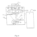
- Fig. 4 is a typical view showing how such a substrate with a thin film are produced.
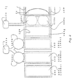
- a film forming chamber is described. Inside a vacuum chamber 16, a film material 3 is placed with its film forming particle generating region 2 turned upward in the drawing.
- An electron beam is emitted from an electron gun 6 to reach the film forming particle generating region 2 due to the effect of a magnetic field not illustrated, to heat the region 2, and as a result, film forming particles 5 are generated.
- the film forming particle flux axis 9 (directional axis to express the direction in which the film forming particles are generated most intensively) of the film forming particles 5 generated like this is turned upward in the drawing.
- a film formation monitor 8 On or near the axial line of the film forming particle flux axis 9, a film formation monitor 8 is installed, and a film thickness measuring instrument 7 for optically measuring the thickness of the film formed on the film formation monitor 8 is installed further above the monitor 8.
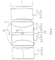
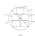
- a hole 401 is formed at the center of a domed substrate holder 402.
- the domed substrate holder 402 can rotate on a horizontal plane above the film forming particle generation source, so that the under surfaces of the substrates 403 on which a film is to be formed, fixed in the domed substrate holder 402 may be exposed to the film forming particles, to form a film on each of them.
- a film forming range limiting member 4 is installed at a position between the film forming particle generating region 2 and the substrates 403 on which a film is to be formed .
- a shutter 11 for intercepting the film forming particles 5 as required is also similarly installed.
- Fig. 5 is a drawing showing this state from the position of the film formation monitor 8 in the direction toward the film forming particle flux axis 9.
- the substrates 403 on which a film is to be formed are arranged, for example as illustrated, to be held by the domed substrate holder by using the available area of the holder to the maximum extent, and the hole 401 is formed on or near the axial line of the film forming particle flux axis 9, to prevent the film forming particles 5 from being intercepted by the substrates, etc.
- the film formation monitor 8 is arranged to allow the film forming particles to reach the film formation monitor 8 through the hole.
- the domed substrate holder 402 is rotated beforehand and kept rotating. Then, the electron beam emitted from the electron gun 6 continuously heats the film forming particle generating region 2 of the film material 3, to generate the film forming particles from there. In this case, at first, since the shutter 11 is closed, the film forming particles cannot reach the substrates on which a film is to be formed. When the temperature of the film forming particle generating region 2 reaches a steady state, the film forming particle generation intensity also reaches a steady state. After this has been confirmed, the shutter 11 is opened.
- the film forming particles generated from the film forming particle generating region 2 are caused to flow radially with the direction of the film forming particle flux axis 9 as the central direction, and reach the respective substrates 403 on which a film is to be formed . Furthermore, through the hole 401 formed on or near the axial line of the film forming particle flux axis 9, some film forming particles reach the film formation monitor 8.
- the thickness of the film formed on each of the respective substrates 403 on which a film is to be formed is indirectly measured by measuring the thickness of the film formed on the film formation monitor 8 by the film thickness measuring instrument 7.
- a film is formed under conditions approximating those for forming the film on each of the respective substrates on which a film to be formed 403. So, the thickness of the thin film formed on the monitor has a certain correlation with the thickness of the thin film formed on each of the respective substrates 403 on which a film is to be formed.
- the thickness of the thin film formed on the monitor is the same as the thickness of the thin film formed on each of the substrates 403 on which a film is to be formed, since the substrates 403 on which a film is to be formed, fixed in the domed substrate holder 402, are exposed incessantly to the film forming particles, like the film formation monitor 8.
- the correlation is strictly obtained by an experiment. From the results, the correlation between the increment per unit time of the thickness of the thin film formed on the film formation monitor 8 and the increment per unit time of the thickness of the thin film formed on each of the substrates 403 on which a film is to be formed is obtained.
- the film forming process control is carried out, such as adjusting the film forming rate during film formation, the refractive index of the films formed, etc., and closing the shutter to terminate film formation when a desired thickness has been reached.
- substrates on which a film to be formed are held by a domed substrate holder rotating around a certain axis (may be virtual).
- a domed substrate holder rotating around a certain axis may be virtual.
- Such a technique is described, for example, in Japanese Patent Laid-Open (Kokai) No. 1-306560.
- a domed substrate holder is similarly used and rotated.
- Fig. 6 is a typical view showing such a continuous production process.
- a loading chamber 601, a film forming chamber 602 and an unloading chamber 603 are connected.
- Substrates on which a film is to be formed are held by a domed substrate holder 604.
- One film forming unit consists of only the substrates on which a film is to be formed held by the domed substrate holder 604.
- Each of the chambers can store one film forming unit.
- the next group of the substrates on which a film is to be formed are supplied into the loading chamber, and the loading chamber is then evacuated. Concurrently, the unloading chamber is opened to the open air, and the substrates with a film formed are unloaded. Then, the unloading chamber is evacuated.
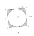
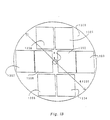
- Fig. 7 is a diagram showing the relation between the film forming area and the moving area of substrates on which a film to be formed.
- the film forming area 701 is usually almost circular.
- a domed substrate holder as large as the circular film forming area 701 is prepared to hold substrates. That is, the film forming area in this case is inside the circular area 701.
- the shaded portions of Fig. 7 can also be used as the film forming area.
- only ⁇ /4 (78.5%) of the area available for film formation is used for production.
- an apparatus which has a circular film forming area with a diameter of 1 m is used to form a film on each of surface antireflection optical filters (26 cm x 33 cm) for displays with a diagonal line length of 14 inches (35 cm).
- This state is seen from the position of the film formation monitor 8 in the direction toward the film forming particle flux axis 9.
- the conventional circular substrate holder is used most effectively, only five optical filters can be held.
- the first reason may be that the properties of the films formed by the film forming particles flying in the direction of and around the film forming particle flux axis are excellent as compared with those of the films formed by the film forming particles flying in any other direction apart from this direction, and that the method was previously believed to be most suitable for monitoring the film forming process.
- the reason for the excellent properties is that since the film forming particles flying in the direction of and around the film forming particle flux axis are large in number and generally have high kinetic energy, the films formed are high in refractive index and homogeneous. On the contrary, the film forming particles flying in any other direction away from the film forming particle flux axis are small in number and low in energy, and the films formed are small in refractive index and thin.
- a conventional apparatus which has overcome the low productivity of the intermittent continuous apparatus with a rotaty transfer type substrate holder is called a feed through type continuous apparatus or in-line apparatus.
- a feed through type film forming apparatus based on sputtering is proposed, for example, in Japanese Patent Laid-Open (Kokai) No. 5-106034, and a similar vacuum evaporator is proposed, for example, in Japanese Patent Laid-Open (Kokai) No. 6-65724.
- the substrate holder (substrates) is once placed in a loading chamber called a load lock chamber, to stand by, and is fed into the film forming chamber intermittently continuously without releasing the vacuum of the film forming chamber.
- the time during which the substrates on which a film to be formed are exposed to vacuum as well as heat until a film is formed on each of them is very short (say, 10 minutes at the longest), and this poses a problem in the case of film formation on resin substrates, etc.
- resin substrates it is often practiced to expose the substrates to heat or vacuum for a longer period of time, for degassing the substrates. If the degassing is not sufficient, such problems often occur that the adhesion between the resin substrate and the vapor-deposited film as adopted in the present invention is insufficient and that the gas evolved from the substrate during film forming process affects the film processing conditions, not allowing a desired film to be obtained.
- a vacuum chamber is arranged additionally on the loading side of the loading chamber, but it makes the apparatus very large (long in the direction in which the substrates on which a film to be formed are fed) disadvantageously in view of space.
- the object of the present invention is to provide a method and apparatus for continuously manufacturing substrates with a thin film, which allow substrates to be smoothly fed by a small apparatus even in the case of multi-layer films, are good in productivity, and allow many kinds (many sizes) of films to be produced by one apparatus, without using large-sized-scale apparatus or causing decline of productivity even if the substrates to have a thin film formed on each of them are large-sized or fed continuously.
- the present invention provides, in order to achieve the above object,: a method according to claim 1 for manufacturing substrate with a thin film, in which a film forming chamber with first and second stockers capable of storing in multi-stages, substrates on which a film is to be formed upstream and downstream of a film forming area is provided, and a loading chamber and an unloading chamber are provided upstream and downstream of the film forming chamber, respectively with a stocker capable of storing in multi-stages, the substrates on which a film is to be formed, wherein while a group of-substrates on which a film to be formed are being subjected to film forming in the film forming chamber, the loading chamber is loaded with the next group of substrates on which a film is to be formed and evacuated, and the substrates which have been previously subjected to film forming are unloaded from the unloading chamber, in which the substrates are being subjected to film forming while passing through the film forming area.
- the substrates on which a film is to be formed are taken out of the first stocker one after another, are passed through the film forming area one after another and are put into the second stocker, and they are taken out of the second stocker one after another, are passed through the film forming area one after another and are put into the first stocker one after another, thus being moved in the sealed chamber repetitively, to be subjected to film forming.
- the speed of passage is substantially constant, to allow the manufacturing of substrates with a homogeneous film formed on each of them.
- the apparatus for executing the method for manufacturing substrate with a thin film is:
- An apparatus comprising a film forming chamber with first and second stockers capable of storing substrates on which a film is to be formed in a plurality of stages upstream and downstream of a film forming area, and a loading chamber and an unloading chamber provided upstream and downstream of said film forming chamber, respectively with a stocker capable of storing, in multi-stages, substrates on which a film is to be formed, wherein said film forming chamber, said loading chamber and said unloading chamber have respectively an independent evacuation means to allow evacuation; and said film forming chamber has a film forming particle generation source, a means for feeding the substrates on which a film to be formed through the film forming area, and means for relocating the substrates on which a film is to be formed one after another from the first stocker into the feeding means and further relocating from the feeding means into the second stocker.
- the substrates on which a film is to be formed preferably used in the present invention can be glass sheets, plastic plates, plastic sheets, plastic films, etc.
- the plastic materials in this case include polymethacrylic acid based resins, polyolefin based resins, polyether based resins, polycarbonate based resins, polyester based resins, polysulfone based resins, polyamide based resins, polysulfide based resins, unsaturated polyester based resins, epoxy based resins, melamine based resins, phenol based resins, diallyl phthalate based resins, polyimide based resins, maleimide based resins, polyphosphazene based resins, urethane based resins, polyvinyl acetate based resins, polyvinyl alcohol based resins, styrene based resins, vinyl chloride based resins, cellulose based resins, diethylene glycol bisallyl carbonate polymer (CR-39),
- the substrates on which a film is to be formed are transparent or translucent.
- a transmittance of about 30 to 70% or with a color selective transmittance it is preferable to use substrates with a transmittance of about 30 to 70% or with a color selective transmittance. A color grayish to an extent not to impair the colors of the display screen is more preferable.
- the present invention is more effective.
- the present invention is suitable for substrates on which a film is to be formed with a short side length of 1/5 or more of the width of the film forming area or 20 cm or more, more suitable for those with a short side length of 26 cm or more.
- the substrates on which a film is to be formed can be arranged in a plurality of rows in the feeding direction, to be exposed to film forming particles simultaneously for having a film formed on each of them.
- the substrates on which a film is to be formed can also be arranged along a curve like a circle, in addition to being arranged like a straight line.
- the substrates on which a film is to be formed can be arranged along a circle and rotated along the circle during film formation, so that the same substrates may pass through the film forming area repetitively.
- the film forming area refers to the area which is exposed to the film forming particles of an amount enough to form thin films on substantially the same plane as the film forming surfaces of substrates on which a film to be formed.
- the film forming area means the total area including the respective regions of the substrates, the gaps between them and the region surrounding them (film forming area 20 in Fig. 9).
- the position where the film formation monitor is fixed in the present invention can be outside the film forming area (that is, for example, the back side of the film forming area limiting member). If this condition is satisfied, the thickness of the film formed on the monitor can be correlated with the film formed on each of the substrates without restricting the arrangement of the substrates to be subjected to film forming. In addition, since there is no intervening object between the film forming particle generation source and the film formation monitor, a thin film equivalent to the thin film formed on each of the substrates on which a film is to be formed can be formed on the monitor, and the film forming process can be controlled accurately.
- the film formation monitor can of course be provided inside the film forming area and outside the substrates on which a film to be formed.
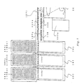
- Fig. 1 shows an embodiment of the method and apparatus for manufacturing substrate with a thin film of the present invention.
- a loading chamber 102, a first stocker chamber 103, a film forming chamber 104, a second stocker chamber 105 and an unloading chamber 106 are arranged to be connected.
- the first stocker chamber 103 and the second stocker chamber 105 are not partitioned from the film forming chamber (as would the possible by, for examples, a gate valve), but are located in the same sealed vacuum housing. So, the first stocker chamber 103 and the second stocker chamber 105 can be considered to be contained in the film forming chamber 104.
- Substrates 109 on which a film is to be formed are held by substrate holders 108.
- One film forming unit consists, for example, of twenty substrate holders 108, and each chamber can store one film forming unit.
- step A An example of the film forming process is described below with attention paid to the feeding of the substrates on which a film is to be formed. The respective steps of the process are described below starting from step A.
- the film forming process in the present invention can also contain the following treatment.
- film formation and treatment can be carried out alternately.
- the treatment in this case can be the treatment of substrates by oxygen plasma, any of various gas plasmas, irradiation with oxygen ions or argon ions, etc. by an ion gun.
- This treatment is used, for example, for the purpose of improving the adhesive strength between a substrate on which a film is to be formed and a film forming material, or between a film forming material and another film forming material, etc.
- the film forming particle generating region 2 of the film forming material 3 is continuously heated by the electronic beam generated from an electron gun 6, to generate film forming particles there.
- a shutter 11 is closed, and the film forming particles cannot reach the substrates on which a film to be formed. If the temperature of the film forming particle generating region 2 reaches a steady state, the film forming particle generation intensity also reaches a steady state. After it has been confirmed, the shutter 11 is opened. After stable film formation has been confirmed on the film formation monitor, the substrate holders 108 are fed from left to right in Fig. 1 at a certain speed. In this case, it is preferable that the speed of passage can be changed based on the information of the film formation monitor.
- the film forming particles generated from the film forming particle generating region 2 fly radially with the direction of a film forming particle bundle axis 9 as the central direction, to reach the respective substrates 109 on which a film is to be formed .
- the thickness of the film formed on the film formation monitor has a certain correlation with the thickness of the film formed on each of the substrates .
- the thickness of the film formed on the film formation monitor 8 is about 20 times the thickness of the film formed on each of the substrates 109.
- this correlation is obtained strictly by an experiment. From the results, the correlation between the increment of the thickness of the film formed on the film formation monitor 8 per unit time and the increment of the thickness of the film formed on each of the substrates 109 per unit time is obtained.
- the film forming rate during film formation, the refractive index of the film formed, etc. are adjusted. After it has been confirmed that, for example, the last 20th one of the substrate holders 108 corresponding to, for example, the last 20th one of the substrates 109 on which a film is to be formed has passed the film forming area, the shutter 11 is closed, to complete film formation in the control of the film forming process.
- the substrate holders 108 are relocated from the first stocker chamber 103 to the feeding means 110 one after another, to be mounted on the feeding means 110, for being fed, and, for example, twenty substrates 109 on which a film is to be formed are exposed to the film forming particles 5, to be subjected to film forming. Then, all the twenty substrate holders 108 are relocated from the feeding means 110 into the second stocker chamber 105, and subsequently, the material of the film forming particle generation source is changed.
- the substrate holders 108 are relocated from the second stocker chamber 105 onto the feeding means 110 one after another in the reverse direction, to be mounted on the feeding means 110, for being fed, and the twenty substrates 109 on which a film is to be formed are exposed to the film forming particles 5. Then, all the twenty substrate holders 108 are relocated from the feeding means 110 into the first stocker chamber 103. This is repeated. If the number of transfer times is even, the substrate holders 108 mounted on the feeding means 110 are not exposed to the film forming particles when fed from left to right in the drawing after the final layer of the film has been formed. Thus, a process as described above can be achieved.
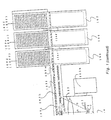
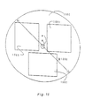
- Fig. 3 illustrates the position at which the film formation monitor is fixed.
- the film formation monitor 8 is the same as in the conventional method for manufacturing substrates with a thin film shown in Fig. 9, except that the film formation monitor 8 is arranged outside the film forming area to measure the thickness of the film formed on the film formation monitor.
- the film formation monitor 8 is located at a position outside the substrate region 20 in the direction perpendicular to both the progression direction of the substrates 310 on which a film is to be formed and the film forming particle flux axis 9. Since the film formation monitor 8 is located at this position, a film can be obtained on each of the substrates 310 on which a film is to be formed , with a size more than double that in Fig. 9.
- the distance between the film formation monitor and the film forming particle generation source can be preferably made closer to the distances between the substrates on which a film is to be formed and the film forming particle generation source.
- the film forming conditions for the film formed on the film formation monitor can be made closer to the film forming conditions for the film formed each of the substrates on which a film is to be formed. Though depending on the intended properties of the film, it is preferable to obtain a film on the film formation monitor which is closer to the films in the substrate region in physical properties such as refractive index, density and electric properties and also in film thickness.
- the position of the monitor is as described in WO 95/33081.
- the film forming process is controlled to adjust such properties as the film forming rate and the refractive index of the films formed during film formation, and to close the shutter 11 when the desired film thickness is achieved.
- the film forming area limiting member is located between the film forming particle generation source and the substrates on which a film is to be formed, and has a function to limit the film forming particle flying range.
- a film forming area limiting member 4 shown in Fig. 1 a plate for limiting the size and form of the film forming area in the substrate progression direction; the film forming area 20 of Fig. 2 is formed like a spool, since the film forming area is limited by a half-moon shaped film forming area limiting member
- the film forming conditions on the film forming particle source side of the film forming area limiting member are equivalent to those in the film forming area.
- the film formation monitor is located at this position for measuring the thickness of the film formed on the film formation monitor, since it is easy to correlate the film thickness with the thickness of the film formed on each of the substrates on which a film is to be formed.
- the film forming area limiting member can also be provided as the film formation monitor to measure the thickness of the film formed there.
- a film is formed on each of the substrates on which a film is to be formed while the substrates are fed through the film forming area means that the substrates on which a film is to be formed are not stopped until their feeding through the film forming area is completed. If they are stopped while they are being fed, they are exposed to film forming particles during different periods of time in the feeding direction, making it difficult to obtain homogeneous films.
- bit-by-bit intermittent movement or a stop for a time short enough not to make partial differences in feeding time is allowed.
- any stop of any duration not to cause any substantial variation in the duration of exposure to the film forming particles in the progression direction is not contrary to the definition that the film is formed on each of the substrates while the substrates are fed through the film forming area.
- the partial difference of feeding time should be 20% or less, though depending on other conditions. A difference of 10% or less is preferable, and 5% or less is more preferable.
- a constant speed is preferable, but if the feeding rate is automatically controlled based on the thickness of the film formed on the film formation monitor, a small speed variation is caused inevitably.
- the thin films formed in the present invention can be of any films, but optical thin films for controlling the reflection or transmittance of light, hard coatings for improving the hardness of the surfaces of plastic substrates, etc., insulation films, conductive films, etc. are preferable.
- optical thin films required to be accurately controlled in thickness are films for which the present invention can be suitably applied.
- antireflection films of various displays are films for which the present invention can be suitably applied, since they mostly use large-sized substrates and are multi-layer films.
- the films of the present invention can be installed on the fronts.
- the present invention can also attract attention as a method to realize antireflection optical filters intended for improving the contrast, preventing the reflection of external light, cutting infrared rays or cutting electromagnetic waves, etc., and also as a method for forming MgO films at a high speed matched with other steps of production in tact time though it is difficult to form such films by sputtering.
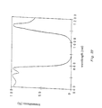
- the thickness of the film formed on the film formation monitor placed inside the film forming particle flux can be measured by the light interference method or energy absorption method, or the change of the monitor in mechanical resonance frequency can be measured, or if the film is electrically conductive, its electric resistance can be measured. If the film is an optical thin film, the light interference method is preferable in view of accuracy of measurement.
- the monitor is irradiated, for example, with light with a specific wavelength, and the reflection intensity or transmission intensity of the light is measured.
- This uses the phenomena that the light interference depends on the refractive index and thickness of the film and that the light reflectance or transmittance changes periodically during film formation. For example, the maximum and minimum reflected light intensities are identified to measure the film thickness.
- the measured result reflects not only the film thickness but also the influence of the refractive index, but this is rather preferable in the case of an optical thin film, since it is often intended to achieve a specific value as the optical path length inside the film, rather than the film thickness itself.
- the interference light intensity has an extremal value when the optical path length in the film (it is proportional to the product of the film thickness and the refractive index) is an integral number of times the 1/4 of the wavelength ⁇ of the measuring light, stopping the film formation when the condition is satisfied assures that the optical path length in the film becomes an integral number of times the 1/4 of the measuring light. Therefore, it allows the film thickness to be measured at higher reproducibility rather than by controlling with reference to the absolute value of the intensity of interfering light.
- the film is more than several micrometers in thickness or low in light transmittance, it is preferable to measure the thickness by measuring the change of the mechanical resonance frequency of a crystal oscillator.
- Film forming processes preferably used in the present invention for generating film forming particles include vacuum evaporation, ion assisted evaporation, ion plating, sputtering and ablation.
- a film material is heated in vacuum to be evaporated or sublimed and the vapor is transported onto substrates on which a film is to be formed which are relatively low in temperature, to be condensed and precipitated, for forming a film on each of them.
- the film material is irradiated on the surface with a charged corpuscular beam such as an electron beam.
- gas ions of oxygen or argon, etc. excited by using an ion gun are acceleratedly applied to substrates on which a film is to be formed for vapor deposition.
- Ion plating is vacuum evaporation executed for potential-biased substrates on which a film is to be formed in a plasma of glow discharge, etc.
- an electrode is placed for the substrates on which a film is to be formed on the side opposite to the film forming particle generation source, to attract particles ionized in a plasma.
- Sputtering is to irradiate the surface of a film material with a high energy corpuscular beam of ions, molecules or atoms, etc. in a vacuum atmosphere, to directly give the energy to the film forming particles (atoms, molecules or their cluster) of the film material, releasing them into the vacuum atmosphere without heating.
- Ablation is to supply similar energy using light.
- These techniques are means for flying film material particles in vacuum, and generate film forming particles widening radially with a specific direction (for example, the direction normal to the surface of the film forming particle generation source, etc.) as the central direction from a film forming particle source.
- the axis of the direction which is the central direction of flying film forming particles is called the film forming particle flux axis.
- the film forming particle flux axis In general, in the direction along the film forming particle flux axis, the largest number of film forming particles fly, and as the angle from the axis becomes larger, the number of film forming particles becomes less, and at the same time, the kinetic energy of the film forming particles tends to be smaller.
- the kinetic energy of film forming particles mostly affects properties such as the refractive index of the film formed on each of the substrates .
- the film formed is higher in refractive index and more homogeneous.
- the direction of flying film forming particles is closer to the direction normal to the film forming direction on the substrate on which a film is to be formed, i.e., to the substrate surface, the refractive index of the film formed is higher. Therefore, the film portion formed in the central portion (near the film forming particle flux axis) of the film forming area has a high refractive index and the film portion nearer to the periphery of the film forming area has a lower refractive index.
- the film thickness becomes also smaller.
- the present invention includes the following methods for controlling the film forming process:
- the thickness of a film formed on a substrate on which a film is to be formed is basically proportional to the product of the number of film forming particles per unit time reaching the surface of the substrate and the time during which the surface stays in the film forming area. Therefore, by adjusting the size of the substrate in the film forming area in progression direction, the thickness of the film formed on the substrate on which a film is to be formed can be controlled.
- One problem is that since the film is formed while the substrate on which a film is to be formed is fed through the film forming area, all the surface of the substrate on which a film to be formed crosses the film forming particle flux, to have a film formed on it. As described above, within the film forming particle flux, the region close to the film forming particle flux axis is different from the periphery in the number of film forming particles, etc. Therefore, in one substrate on which a film is to be formed, the region which passes at and near the film forming particle flux axis and the region which passes the periphery only are different in thickness and physical properties even if they are exposed to the film forming area for the same period of time. So, as in the film forming area 20 shown in Fig.
- the film forming area is formed like a spool.
- a film forming area limiting member formed like a half-moon in the flying route of the film forming particles, to define the form of the film forming area like a spool with arcs in the progression direction of the substrate.
- the film forming area limiting member is manufactured at first, for example, based on the cosine law (the law that the thickness of the film formed is proportional to the third or fourth power of the cosine of the angle formed between the film forming particle flying direction and the film forming particle flux axis), and is used to repeat film forming experiments until satisfactory film thickness and refractive index distributions are obtained, for finally deciding the optimum form.
- the control of film forming process by using the method (2) is described below. specifically this is to change the travelling speed of the substrate on which a film to be formed depending on the thickness of the film formed on the film formation monitor. This is to control the length of time during which the surface of the substrate on which a film is to be formed is exposed to film forming particles, like the method (1).
- the amount of film forming particles flying from a film forming source or its kinetic energy depends on the states of the vacuum vessel such as vacuum degree and the contamination of the vessel, and the effect of degassing from supplied substrates.
- the film speed of passage is adjusted while the change of the thickness of the film formed on the film formation monitor (i.e., film forming rate) is monitored. For example, such control is preferable that if the film forming rate is high, the substrate speed of passage is raised, and that on the contrary if the film forming rate is low, the substrate speed of passage is lowered.
- the control of film forming process using the method (3) is described below.
- the energy applied to the generation source is adjusted depending on the thickness of the film formed on the film formation monitor.
- the adjustment allows the number of film forming particles per unit time reaching the film forming area and the energy of film forming particles to be controlled.
- the film forming process can be controlled in such a manner that the filament current of the electron gun is made smaller if the film forming rate is high, and that the filament current of the electron gun is made larger if the film forming rate is low.
- This method also allows the feedback control of the process by measuring the thickness of the film formed on the film formation monitor.
- the control of film forming process by using the method (4) is described below. Even if the number of film forming particles reaching the film forming area is the same, a higher surface temperature of the substrate on which a film is to be formed results in a higher film forming rate and may result in a higher refractive index, depending on the kind of the film formed. This nature can be used to control the film forming process such as film forming rate, refractive index, etc. by adjusting the surface temperature of the substrate on which a film is to be formed.
- the heater preferably used in this case can be a halogen lamp using the radiation of light, or a sheath heater (micro heater) or nichrome heater mainly intended for infrared radiation and thermal conduction.
- the controller used can be of on-off control type, but a controller allowing PID control can be preferably used.
- the film forming rate of the film forming process is preferable to measure the film forming rate of the film forming process by monitoring the thickness of the film formed on the film formation monitor, and to control the film forming process based on the obtained film forming rate.
- the film forming rate has a correlation with the physical properties of the film formed. For example, in the formation of a TiO 2 film, TiO 2 in its molten state at a film forming particle generation source becomes Ti 3 O 5 to fly in vacuum, and during flying or on the substrate, it causes oxidation-reduction reaction with O 2 , to form a TiO 2 film. The oxidation-reduction reaction is greatly affected by the kinetic energy of Ti 3 O 5 particles.
- the kinetic energy of film forming particles is a physical quantity with a correlation with the flying velocity of the film forming particles, and has an intense correlation with the film forming rate.
- the inventors found that a thin film with preferable physical properties can be formed by controlling the film forming rate. For example, at a specific film forming rate, an unabsorbable film with a high refractive index can be formed in some cases. In such cases, it is preferable to stabilize the film forming rate at an optimum value. Furthermore, if the film forming rate is changed periodically, the physical properties of the film can be changed periodically in other cases.
- the film materials which can be controlled in physical properties by specifying the film forming rate include ITO (indium tin oxide), SnO 2 , In 2 O 3 , ZnO, MgO, etc. respectively recently used in LCDs, etc.
- a preferable method for controlling the film thickness distribution and the film performance distribution is to specially design the film forming particle generation source. That is, to keep the film thickness distribution and the film performance distribution constant over time, it is preferable to move the film forming particle generating material to the film forming particle generating region continuously at a certain speed, for eliminating the temporal change in the form of the molten portion. This assures that the optical thin films required to be highly accurate such as antireflection optical filters have a uniform film thickness distribution and a uniform performance distribution in the progression direction of substrates on which a film is to be formed.
- the distances between the substrates on which a film is to be formed and the film forming particle generation source are 500 mm or more. Distances of 800 mm or more are more preferable. If the distances are shorter than 500 mm, the resin substrates may be greatly affected and damaged by the radiation heat from the film forming particle generation source in some cases. In the case of ITO films or MgO films, etc., reactive vapor deposition is often used, but due to insufficient reaction with oxygen gas, color absorbable films may be formed in some cases. Furthermore, because of the likelihood of being affected by the dispersion of the film forming particle generation source, unevenness in film thickness may also be caused.
- stockers are installed in a film forming chamber.
- the substrates can be sufficiently heated and degassed to have a film with excellent physical properties to be formed on each of them since the substrates on which a film is to be formed can be kept in a high vacuum area for a long period of time.
- the substrates on which a film to be formed can pass smoothly.
- the plurality of stages are perpendicular to the direction in which the substrates on which a film is to be formed are fed through the film forming area, and that the direction in which the substrates on which a film is to be formed are relocated to and from agrees with the direction in which the substrates on which a film is to be formed are passed through the film forming area.
- the direction in which the plurality of stages are arranged in the stocker, the direction in which the substrates on which a film is to be formed are relocated to and from the stocker and the direction in which the substrates on which a film is to be formed are passed through the film forming area are three-dimensional (in three axial directions), a complicated mechanism is necessary for changing the direction of the substrates on which a film is to be formed, and since the mechanism must be kept in vaccum, the vacuum seal of the drive is very difficult.
- the plurality of stages are perpendicular to the direction in which the substrates on which a film is to be formed are passed through the film forming area, and the direction in which the substrates on which a film is to be formed are relocated to and from are the same as the direction in which the substrates on which a film is to be formed are passed through the film forming area.
- the substrates can be relocated with the retainer of substrates (substrate holders) in the multi-stage stocker kept almost at the same level as the retainers used for relocating the substrates (substrate holders) to or from the stocker, and if the substrates (substrate holders) are fed in the direction in which they are relocated from, they can be exposed to the film forming area, to allow a reasonable mechanism to be adopted.
- the stocker is driven vertically to relocate the substrates (substrate holders) horizontally while the substrates (substrate holders) are fed through the film forming area horizontally is described below.
- the stocker has a structure to receive a substrate (substrate holder) at sides XY and ZW shown in Fig. 24 and the direction in which the substrate is relocated to and from the stocker agrees with the direction in which the substrate is fed through the film forming area, with rollers arranged in this direction, then the substrate (substrate holder) vertically moved by the stocker can be received by the rollers at the illustrated sides XW and YZ. So, the substrates can be relocated very smoothly advantageously. Furthermore, since the vacuum seal is required for the drive shaft used for vertical driving and the drive shaft used for horizontal carrying, design is very easy and maintenance is also easy. Moreover, troubles are unlikely to occur in production.
- the substrates are carried horizontally by rollers, and the rollers can be driven by a servo motor. So, the substrate carrying speed can be set very accurately. Furthermore, such speed control as to accelerate the substrates (substrate holders) before the film forming area, and to keep the speed constant in the film forming area, and then to accelerate after the film forming area, for subsequent deceleration is also very easy. Therefore, it is very preferable to use this structure.
- the method for heating the substrates in the present invention it is preferable to heat in the film forming chamber and in the loading or unloading chamber upstream or downstream of it, or to heat in the loading or unloading chamber only, or to heat in all the chambers.
- the structure of the stocker has substrate portions, heater portions, substrate portions and heater portions arranged alternately. It is preferable to adopt this structure in the stockers upstream and downstream of the film forming area in the film forming chamber and also in the loading or unloading chamber, or further in the loading or unloading chamber upstream and downstream thereof.
- the film forming chamber is equipped with a means which allows the process conditions to be changed.
- a gas introducing means is equipped with a device to allow the gas volume to be adjusted.
- the vacuum degree can be changed for forming each layer.
- the refractive index of the film can be controlled or changed often by the vacuum pressure acting during film formation.
- a thin film like ZrO 2 film is a good example.
- the means as described above is very effective.
- an electron gun as their evaporation means can be used commonly, depending on cases, and this is very advantageous in view of cost reduction of apparatus. Furthermore, it is very preferable if process conditions can be changed within the same evacuation mechanism with high vacuum kept, since different kinds of treatment can be carried out in the same vacuum chamber.
- a multi-layer film formed by repeating the actions of exposing a film once fed through a vacuum treatment apparatus to the open air and feeding the film again through the vacuum treatment apparatus causes peeling in a cross-hatched film peeling test, but a multi-layer film obtained by treating in a film forming chamber with stockers in vacuum according to the present invention is good in adhesion between layers, and does not pose any problem in the same cross-hatched film peeling test.
- the outermost layer is often treated to be water repellent for prevention of contamination.
- a material impregnated with a fluorine based organic solution is used for vapor deposition.
- the film forming apparatus shown in Fig. 1 was used to form a thin film on each of substrates on which a film to be formed, for manufacturing substrate with a thin film.
- the substrate with a thin film were intended to be used as antireflection filters of displays, and the thin films were optical thin films requiring strict film thickness control.
- the film forming process was vacuum evaporation, ion assisted evaporation or high frequency ion plating.
- the substrates on which a film is to be formed which more used were made of a transparent plastic material.
- the film forming area had a width of 1200 mm.
- the installation area of the apparatus was about 100 m 2 , and two operators were necessary for operating the apparatus. Since the number of film forming chambers was one, the number of evacuation pumps could also be one, and it was not necessary to prepare many electron guns as means for generating film forming particles. So, the apparatus could be very low in cost.
- the film formation monitor was arranged outside the film forming area, to eliminate the influence of the substrate size.
- the distance between the film formation monitor and the film forming particle generation source was longer than the shortest distance between the film forming area and said generation source and shorter than the longest distance.
- the direction normal to the film formation monitor agreed with the direction in which the film forming particles flew at the position of the film formation monitor.
- the thickness of the film formed on the film formation monitor was measured by using both a light interference type film thickness meter and a quartz type film thickness meter.
- the film composition was as shown in Table 1. The film forming process is described below.
- One tact time for forming a film on each substrate of the twenty groups of substrates on which a film is to be formed obtained by adding mechanical loss time to the time of steps (1) through (5) was 30 minutes.
- the tact cycle of operation was repeated 140 times, and the time taken for the operation including the initial evacuation and final unloading was 72 hours (3 days).
- 11,200 surface antireflection filters of displays of 14 inches (35 cm) were produced (20 holders x 4 substrates x 140 times).
- An apparatus shown in Fig. 6 similar to the continuous vacuum thin film forming apparatus described in Japanese Patent Laid-Open (Kokai) No. 3-193873 was used to form a thin film on each of substrates on which a film is to be formed, for manufacturing substrate with a thin film.
- the substrates with a thin film were intended to be used as antireflection filters of displays, and the thin films were optical thin films requiring strict film thickness control.
- the film forming process was vacuum evaporation, and the substrates on which a film is to be formed were made of a transparent plastic material.
- the film forming area had a width of 1200 mm. That is, an apparatus capable of forming a film forming area with a width of 1200 mm was used.
- the installation area of the apparatus was about 100 m 2 , and two operators were necessary for operating the apparatus.
- the film formation monitor was placed at the center of a domed substrate holder as shown in Fig. 4, and the domed substrate holder had a hole at the center.
- the thickness of the film formed on the film formation monitor was measured by using a light interference type instrument.
- the film composition was as shown in Table 1. The film formation process is described below.
- One tact time for forming a film on each of the eight substrates obtained by adding mechanical loss time to the time of steps (0) through (5) was 18 minutes.
- the tact cycle of operation was repeated 235 times, and the time taken for the operation including the initial evacuation and the final unloading was 72 hours (3 days).
- 1,880 surface antireflection filters (8 substrates x 235 times) of displays of 14 inches (35 cm) were produced.
- Example 1 Compared to Example 1, even though the size of apparatus and the number of operators were the same, the productivity of Example 1 was as high as about 6 times that of Comparative Example 1 (11,200 films/1,880 films a 6 times). From substrate Layer forming material Physical layer thicness 1st layer ZrO2 Approx.25nm 2nd layer SiO2 Approx.20nm 3rd layer I.T.O Approx.30nm 4th layer TiO2 Approx.85nm 5th layer SiO2 Approx.87nm
- Example 1 Films were formed as described in Example 1, except that three substrates on which a film is to be formed (310 mm x 380 mm x 2 mm) for surface antireflection filters of displays of 17 inches (43 cm) different in size from those used in Example 1 were used. The size of the substrate holders was remained the same as 500 mm x 1200 mm. The state is shown in Fig. 11.
- the tact cycle of operation was repeated 140 times, and the time taken for the operation including initial evacuation and final unloading was 72 hours (3 days).
- 8,400 surface antireflection filters (20 holders x 3 substrates x 140 times) of displays of 17 inches (43 cm) were produced.
- Example 2 The productivity of Example 2 was as high as about 7 times that of Comparative Example 2 (8,400 films/1,175 films a 7 times).
- Films were formed as described in Example 1, except that two substrates on which a film is to be formed (380 mm x 460 mm x 2 mm) for surface antireflection filters of displays of 20 inches (51 cm) different in size from those used in Example 1 were used.
- the size of the substrate holders was remained the same as 500 mm x 1200 mm. The state is shown in Fig. 12.
- the tact cycle of operation was repeated 140 times, and the time taken for the operation including initial evacuation and final unloading was 72 hours (3 days).
- 5600 surface antireflection filters (20 holders x 2 substrates x 140 times) of displays of 20 inches (51 cm) were produced.
- This tact cycle of operation was repeated 235 times, and the time taken for the operation including initial evacuation and final unloading was 72 hours (3 days).
- 705 surface antireflection filters (3 substrates x 235 times) of displays of 20 inches (51 cm) were produced.
- Example 3 The productivity of Example 3 was as high as about 8 times that of Comparative Example 3 (5,600 films/705 films a 8 times).
- the film forming apparatus shown in Fig. 1 was used to form a thin film on each of substrates on which a film is to be formed, for manufacturing substrates with a thin film.
- the substrates with a thin film were intended to be used as near infrared reflection mirrors, and the thin films were optical thin films requiring strict film thickness control.
- the film forming process was vacuum evaporation or ion assisted evaporation.
- the substrates on which a film is to be formed were made of a transparent plastic material.
- the film forming area had a width of 1200 mm.
- the installation area of the apparatus was about 100 m 2 and two operators were necessary for operating the apparatus.
- the film formation monitor was placed outside the film forming area to eliminate the influence on the substrate size.
- the distance between the film formation monitor and the film forming particle generation source was longer than the shortest distance between the film forming area and the generation source and shorter than the longest distance, and the direction normal to the film formation monitor agreed with the direction in which the film forming particles flew at the position of the film formation monitor.
- the thickness of the film formed on the film formation monitor was measured using both a light interference type optical film thickness meter and a quartz type film thickness meter.
- the film composition was as shown in Table 3. The film forming process is described below.
- One transparent substrate of PMMA (450 mm x 1150 mm x 2 mm) for a near infrared reflection mirror hard-coated on both sides with an ultraviolet setting acrylic resin was set on one holder of substrate on which a film is to be formed (500 mm x 1200 mm). Twenty substrate holders of this type were prepared to hold 20 substrates in total. The substrates were heated to 80°C by micro heaters and halogen lamps.
- the large-sized film forming apparatus shown in Fig. 1 was used to form a thin film on each of substrates on which a film is to be formed, for manufacturing substrates with a thin film.
- the substrates with a thin film were intended to be used as antireflection filters of displays, and the thin films were optical thin films requiring strict film thickness control.
- the film forming process was vacuum evaporation, ion assisted evaporation or high frequency ion plating, and the substrates on which a film is to be formed were made of a transparent plastic material.
- the film forming area had a width of 1200 mm.
- the installation area of the apparatus was about 140 m 2 , and two operators were necessary for operating the apparatus. Since the number of film forming chambers was one, the number of evacuation pumps could also be one, and it was not necessary to prepare many electron guns as means for generating film forming particles. So, the apparatus could be very low in cost.
- the film formation monitor was arranged outside the film forming area, to eliminate the influence on the substrate size.
- the distance between the film formation monitor and the film forming particle generation source was longer than the shortest distance between the film forming area and the generation source and shorter than the longest distance, and the direction normal to the film formation monitor agreed with the direction in which the film forming particles flew at the position of the film formation monitor.
- the thickness of the film formed on the film formation monitor was measured using both a light interference type optical film thickness meter and a quartz type film thickness meter.
- the film composition was as shown in Table 1. The film forming process is described below.
- the substrate was a grayish colored substrate with selective transmittability of three primary colors (red, green and blue) at a transmittance of 70%.
- Sixteen substrate holders of this type were prepared to hold sixteen substrates on which a film is to be formed in total.
- the film forming conditions were as described in Example 1, except that the feed distance per once was different and that the time taken for forming one film was different.
- a roll of steel wool #0000 was rubbed against a sample with a load of 2 kg applied, in the directions in parallel and perpendicular to the fibers of the steel wool.
- the abrasion resistance was evaluated according to the following criterion: A : Not flawed at all B : Slightly flawed C : A little flawed D : Heavily flawed
- a sample was cut in by a razor to form one hundred 1 mm meshes.
- a cellophane adhesive tape was stuck onto the portion of 100 meshes, and removed at a time. The number of meshes remaining on the sample was counted for evaluation.
- Gauze impregnated with a marketed glass cleaner was rubbed against a sample with a load of 2 kg applied, 2000 times, to observe the appearance such as film peeling under transmitted light.
- a tester was used to apply a probe with a width of 1 cm to the surface of a sample for measuring the electric resistance.
- a sample with a surface resistance of 5 k1 ⁇ 2 or less was acceptable.
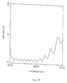
- a spectrophotometer (Hitachi Model 330) was used for measurement.
- a spectral characteristic in a wavelength range of 400 nm to 800 nm was measured, and in the case of a near infrared reflection filter, a spectral transmittance characteristic in a wavelength range of 600 nm to 1200 nm was measured.
- the method and apparatus for manufacturing substrate with a thin film of the present invention even when a thin multi-layer film is formed on each of large-sized substrates on which a film is to be formed, thin films and substrate with a thin film can be continuously produced using a smaller inexpensive manufacturing apparatus. Since the apparatus is small in installation space, it is effective for saving the space of the factory.
- the method and apparatus for manufacturing substrates with a thin film of the present invention is very effective especially when the substrates are made of a resin, and desired films are liable to be obtained, and physical properties such as film adhesion are very good.
- the thin films obtained are less likely to be irregular in the feed direction of substrates.
- the substrates on which a film is to be formed can be arranged at a high degree of freedom, to improve the productivity of the substrates with a thin film manufacturing process.
- the film formed in the film formation monitor since the film formed in the film formation monitor has properties close to those of the thin film formed on each of the substrates , the film thickness can be accurately controlled.
- the film forming process is controlled based on the film forming rate of the film formed on the film formation monitor, the physical properties of the thin films produced can be accurately controlled.
Abstract
Description
- 1a-d:
- substrate on which a film is to be formed
- 2:
- film forming particle generating region 3: film material
- 4a, b:
- film forming area limiting member
- 5:
- film forming particle 6: electron gun
- 7:
- film thickness measuring instrument
- 8:
- film formation monitor 9: film forming particle flux axis
- 10a-d':
- substrate on which a film is to be formed
- 11:
- shutter 16: vacuum chamber 20: film forming area
- 101, 102:
- loading chamber 103: stocker chamber
- 104:
- film forming chamber 105: stocker chamber
- 106, 107:
- unloading chamber 108: substrate holder
- 108a-f:
- a group of substrate holders
- 109a-m:
- a group of substrates on which a film is to be formed
- 110:
- feeding means 111: substrate heating means
- 112:
- antenna for high frequency plasma generation
- 113a-h:
- vacuum pump 114a-d: gate valve
- 211a-b:
- ion gun 212a-d: oil-sealed rotary pump
- 218a-b:
- film formation monitor
- 310a-d:
- substrate on which a film is to be formed
- 310b:
- substrate on which a film is to be formed
- 310c:
- substrate on which a film to be formed
- 310d:
- substrate on which a film is to be formed
- 401:
- hole 402: domed substrate holder
- 403a-g:
- substrate on which a film is to be formed
- 404:
- vacuum pump 601: loading chamber
- 602:
- film forming chamber 603: unloading chamber
- 604a-b:
- substrate holder 604c: substrate holder
- 605a-c:
- a group of substrates on which a film is to be formed
- 606a-d:
- gate valve 701: circular film forming area
- 800:
- circular substrate holder
- 801-805:
- substrate on which a film is to be formed
- 1000:
- substrate holder
- 1101-1103:
- substrate on which a film is to be formed
- 1200:
- substrate holder
- 1201-1202:
- substrate on which a film is to be formed
- 1300:
- circular substrate holder
- 1301-1308:
- substrate on which a film is to be formed
- 1400:
- circular substrate holder
- 1401-1405:
- substrate on which a film is to be formed
- 1500:
- circular substrate holder
- 1501-1503:
- substrate on which a film is to be formed
| From substrate | Layer forming material | Physical layer thicness |
| 1st layer | ZrO2 | Approx.25nm |
| 2nd layer | SiO2 | Approx.20nm |
| 3rd layer | I.T.O | Approx.30nm |
| 4th layer | TiO2 | Approx.85nm |
| 5th layer | SiO2 | Approx.87nm |
| From substrate | Layer forming | Optical layer material thickness |
| 1st layer | SiO2 | Approx.225nm |
| 2nd layer | TiO2 | Approx.225nm |
| 3rd layer | SiO2 | Approx.225nm |
| 4th layer | TiO2 | Approx.225nm |
| 5th layer | SiO2 | Approx.225nm |
| 6th layer | TiO2 | Approx.225nm |
| 7th layer | SiO2 | Approx.225nm |
| 8th layer | TiO2 | Approx.225nm |
| 9th layer | SiO2 | Approx.225nm |
| 10th layer | TiO2 | Approx.225nm |
| 11th layer | SiO2 | Approx.225nm |
| 12th layer | TiO2 | Approx.225nm |
| 13th layer | SiO2 | Approx 225nm |
| 14th layer | TiO2 | Approx.225nm |
| 15th layer | SiO2 | Approx.113nm |

Claims (51)
- A method for forming a thin film on a substrate (1), in which there is provided a film forming chamber (104) having, upstream and downstream of a film forming area, respective first and second stockers (103,105) capable of storing, in multi-stages, substrates (1) on which, respectively, a film is to be formed and has been formed, and in which there is provided, upstream and downstream respectively of the film forming chamber (104), a loading chamber (102) and an unloading chamber (106) provided with respective said first and second stockers (103,105), wherein while a group of substrates (1) on which a film is to be formed is being subjected to film forming in the film forming chamber (104), the loading chamber (102) is loaded with the next group of substrates (1) on which a film is to be formed and evacuated, and the substrates (1) which have been previously subjected to film forming are unloaded from the unloading chamber (106), in which the substrates (1) are being subjected to film forming while passing through the film forming area.
- A method according to claim 1, wherein the substrates on which respective films are to be formed are taken out of the first stocker (103) one after another, are passed through the film forming area one after another and are put into the second stocker (105) one after another, and they are taken out of the second stocker (105) one after another, are passed through the film forming area one after another and are put into the first stocker (103) one after another, thus being moved in the sealed chamber repetitively, to be subjected to film forming.
- A methods according to claim 1 or claim 2, wherein the speed of passage is substantially constant.
- A method according to claim 2 or claim 3, wherein particles of a film forming material are provided by a particle generation source and a first film layer is formed on a substrate from particles of a first film forming material and, after the first film layer has been once formed, particles of the first film forming material are exchanged for particles of a second film forming material, while maintaining the film forming chamber at a reduced pressure, and the substrate on which the first film layer has been formed is again passed through the film forming area, to form a film of two or more layers.
- A method according to any one of claims 1 to 4, wherein two or more film forming particle generating materials are provided in the film forming chamber (104), and the substrates are moved from the first stocker (103) to the second stocker (105), to form a film of two or more layers by a single passage.
- A method according to any one of claims 1 to 5, wherein a second loading chamber (101) is provided upstream of the loading chamber (102) and is loaded with a group of substrates on which a film is to be formed to be fed after a previous group and evacuated while a group of substrates on which a film is to be formed is being subjected to film forming in the film forming chamber (104).
- A method according to any one of claims 1 to 6, wherein a second unloading chamber (107) is provided downstream of the unloading chamber (106), to allow a substrate on which a film has been formed by subjecting it to film forming in the previous step to be relocated from the unloading chamber (106) to the second unloading chamber (107) and to allow a substrate on which a film has been formed by subjecting it to film forming in the step before the previous step to be unloaded from the second unloading chamber (107) while a group of substrates on which a film to be formed is being subjected to film forming in the film forming chamber (104).
- A method according to any one of claims 1 to 7, wherein the loading chamber (102) is heated.
- A method according to any one of claims 1 to 8, wherein films are formed in the film forming chamber (104) while the film forming process is controlled in dependence upon the thickness of the film formed on a film formation monitor.
- A method according to claim 9, wherein the film forming process is controlled by changing any one of the temperature of the substrate on which a film is to be formed, vacuum degree, length of film forming area, speed of passage of substrate on which a film is to be formed and density of film forming particles or a combination thereof during film formation.
- A method according to claim 10, wherein the film forming process is controlled by changing the temperature of the substrate on which a film is to be formed.
- A method according to claim 10, wherein the film forming process is controlled by changing the vacuum degree.
- A method according to claim 10, wherein the film forming process is controlled by changing the length of the film forming area.
- A method according to claim 10, wherein the film forming process is controlled by changing the speed of passage of the substrate on which a film is to be formed.
- A method according to claim 10, wherein the film forming process is controlled by changing the density of the film forming particles.
- A method according to any one of claims 9 to 15, wherein the film formation monitor is arranged within the film forming area but outside the substrate region.
- A method according to any one of claims 9 to 16, wherein a film forming area limiting member is provided in the film forming chamber, and the film formation monitor is arranged between the film forming area limiting member and the film forming particle generation source.
- A method according to any one of claims 9 to 17, wherein the film formation monitor is moved in the film forming area during film formation.
- A method according to any one of claims 9 to 18, wherein the film forming rate is measured by monitoring the thickness of the film formed on the film formation monitor, and the film forming process is controlled in dependence upon the film forming rate.
- A method according to any one of claims 9 to 19, wherein films are formed while maintaining the film forming rate constant.
- A method according to any one of claims 9 to 19, wherein the method for detecting the thickness of the film formed on the film forming monitor is a light interference method.
- A method according to any one of claims 1 to 21, wherein the film forming method is any one of vacuum evaporation, ion assisted evaporation, ion plating and sputtering.
- A method according to any one of claims 1 to 22, wherein during film formation, a film forming particle generating material is continuously supplied to a film forming particle generating region.
- A method according to any one of claims 1 to 23, wherein the substrates having a thin film thereon are surface antireflection filter substrates of displays.
- A method according to any one of claims 1 to 23, wherein the substrates having a thin film thereon are color filter substrates for liquid crystal.
- A method according to any one of claims 1 to 23, wherein the substrates having a thin film thereon are substrates for transparent electrodes.
- A method according to any one of claims 1 to 23, wherein the substrates having a thin film thereon are front panels of plasma display panels.
- A method according to any one of claims 1 to 23, wherein the substrates having a thin film thereon are MgO substrates on which a film is formed, used in plasma display panels.
- A method according to any one of claims 1 to 23, wherein the substrate having a thin film thereon is a band pass filter substrate.
- A method according to any one of claims 1 to 23, wherein the substrates having a thin film thereon are optical lenses.
- An apparatus comprising a film forming chamber (104) having, upstream and downstream of a film forming area, respective first and second stockers (103,105) capable of storing, in multi-stages, substrates on which, respectively, a film is to be formed and has been formed and, upstream and downstream of the film forming chamber (104), a loading chamber (102) and an unloading chamber (106), which loading and unloading chambers (104,106) are provided with respective said first and second stockers (103,105), wherein the film forming chamber (104), the loading chamber (102) and the unloading chamber (106) have respectively an evacuation means capable of evacuation independently; and the film forming chamber (104) has a film forming particle generation source, a means for passing a substrate on which a film is to be formed through the film forming area, and means for taking out a substrate on which a film has been formed one after another from the first stocker (103) into the passing means and further transferring the substrate from the passing means into the second stocker (105).
- An apparatus according to claim 31, wherein the film forming chamber (104) has means for taking out a substrate on which a film has been formed and an additional film is to be formed one after another from the second stocker (105) to the passing means and transferring the substrate from the passing means into the first stocker (103).
- An apparatus according to claim 31 or claim 32, wherein the multi-stage stockers (103, 105), loading chamber (102) and unloading chamber (106) are disposed relative to one another and to the film forming area such that a substrate on which a film is to be formed is passed through the film forming area in a direction (a) and is thereafter relocated in the same direction (a) and wherein each of the multi-stage stockers (103,105) has a structure in which the plurality of stages are provided perpendicularly to the direction (a).
- An apparatus according to any one of claims 31 to 33, having a means for exchanging the film forming particle generation source while maintaining the film forming chamber (104) at a reduced pressure.
- An apparatus according to any one of claims 31 to 34, wherein the film forming particle generation source is a cathode.
- An apparatus according to any one of claims 31 to 34, wherein the film forming particle generation source is an electron gun.
- An apparatus according to any one of claims 31 to 34, having a film formation monitor provided within the film forming area but outside the substrate region.
- An apparatus according to any one of claims 31 to 37, having a film formation monitor capable of moving in the film forming area.
- An apparatus according to any one of claims 31 to 38, wherein an optical film thickness meter using light interference is used as a film formation monitor.
- An apparatus according to any one of claims 31 to 39, wherein the distance between the substrate on which a film is to be formed and the film forming particle generation source is 800 mm or more.
- An apparatus according to any one of claims 31 to 40, wherein a second loading chamber (101) capable of being evacuated independently and with a stocker capable of storing, in multi-stages, substrates on which a film is to be formed is provided additionally upstream of the loading chamber (102).
- An apparatus according to any one of claims 31 to 41, wherein a second unloading chamber (107) capable of being evacuated independently and with a stocker capable of storing, in multi-stages, substrates on which a film is to be formed is provided additionally downstream of the unloading chamber (106).
- An apparatus according to any one of claims 31 to 42, wherein the loading chamber (102) has a heating means.
- An apparatus according to any one of claims 31 to 43, wherein the film forming chamber (104) contains a film forming area limiting member between the film forming particle generation source and a plane in which the substrate on which a film is to be formed travel.
- An apparatus according to claim 44, wherein during film formation, the film forming area limiting member can be moved.
- An apparatus according to claim 44 or claim 45, wherein two or more film forming area limiting members are provided and can be exchanged during film formation.
- An apparatus according to any one of claims 31 to 46, wherein the speed of passage of the substrate on which a film is to be formed can be changed during film formation.
- An apparatus according to any one of claims 31 to 47, having a means for keeping the speed at which the substrates on which a film is to be formed are passed through the area, constant during film formation, and a means for accelerating the speed of passage of the substrate on which a film is to be formed after it has passed through the film forming area.
- An apparatus according to any one of claims 31 to 48, wherein the output of the film forming particle generation source can be changed during film formation.
- An apparatus according to any one of claims 31 to 49, wherein the temperature of the substrates on which a film is to be formed can be changed during film formation.
- An apparatus according to any one of claims 31 to 50, wherein a film forming particle generating material can be continuously supplied to a film forming particle generating region during film formation.
Applications Claiming Priority (4)
| Application Number | Priority Date | Filing Date | Title |
|---|---|---|---|
| JP78840/96 | 1996-04-01 | ||
| JP7884096 | 1996-04-01 | ||
| JP7884096 | 1996-04-01 | ||
| PCT/JP1997/001054 WO1997037051A1 (en) | 1996-04-01 | 1997-03-27 | Method of manufacturing substrate with thin film, and manufacturing apparatus |
Publications (3)
| Publication Number | Publication Date |
|---|---|
| EP0834596A1 EP0834596A1 (en) | 1998-04-08 |
| EP0834596A4 EP0834596A4 (en) | 2003-03-26 |
| EP0834596B1 true EP0834596B1 (en) | 2004-08-11 |
Family
ID=13673031
Family Applications (1)
| Application Number | Title | Priority Date | Filing Date |
|---|---|---|---|
| EP97908528A Expired - Lifetime EP0834596B1 (en) | 1996-04-01 | 1997-03-27 | Method of manufacturing substrate with thin film, and manufacturing apparatus |
Country Status (7)
| Country | Link |
|---|---|
| US (1) | US5993614A (en) |
| EP (1) | EP0834596B1 (en) |
| KR (1) | KR19990022135A (en) |
| AT (1) | ATE273403T1 (en) |
| DE (1) | DE69730185T2 (en) |
| TW (1) | TW320687B (en) |
| WO (1) | WO1997037051A1 (en) |
Families Citing this family (37)
| Publication number | Priority date | Publication date | Assignee | Title |
|---|---|---|---|---|
| JP3370806B2 (en) * | 1994-11-25 | 2003-01-27 | 株式会社半導体エネルギー研究所 | Method for manufacturing MIS type semiconductor device |
| US6275744B1 (en) * | 1997-08-01 | 2001-08-14 | Kokusai Electric Co., Ltd. | Substrate feed control |
| US6556189B1 (en) * | 1998-04-24 | 2003-04-29 | Nissha Printing Co., Ltd. | Touch panel device |
| US20020099886A1 (en) * | 1999-05-17 | 2002-07-25 | Emerson Theodore F. | System and method for controlling remote console functionality assist logic |
| JP4345158B2 (en) | 1999-10-15 | 2009-10-14 | ソニー株式会社 | Optical component manufacturing apparatus and manufacturing method |
| KR100323991B1 (en) * | 1999-11-16 | 2002-02-16 | 이경희 | Thin layer film fabrication method and it's fabrication machine |
| TW490714B (en) | 1999-12-27 | 2002-06-11 | Semiconductor Energy Lab | Film formation apparatus and method for forming a film |
| US20020011205A1 (en) | 2000-05-02 | 2002-01-31 | Shunpei Yamazaki | Film-forming apparatus, method of cleaning the same, and method of manufacturing a light-emitting device |
| US6881269B2 (en) * | 2000-08-17 | 2005-04-19 | Novartis Ag | Lens plasma coating system |
| EP1376162A4 (en) * | 2001-02-27 | 2008-11-26 | Seiko Epson Corp | Multi-layer film cut filter and production method therefor, uv cut filter, dustproof glass, display panel and projection type display unit |
| JP2002363733A (en) * | 2001-06-04 | 2002-12-18 | Nippon Sheet Glass Co Ltd | Method of forming coating film |
| JP4120546B2 (en) * | 2002-10-04 | 2008-07-16 | 株式会社Ihi | Thin film forming method and apparatus, solar cell manufacturing method and apparatus, and solar cell |
| US20040121146A1 (en) * | 2002-12-20 | 2004-06-24 | Xiao-Ming He | Composite barrier films and method |
| JP4476073B2 (en) * | 2004-04-08 | 2010-06-09 | 東北パイオニア株式会社 | Method and apparatus for manufacturing organic EL element |
| JP2006058473A (en) * | 2004-08-18 | 2006-03-02 | Oyokoden Lab Co Ltd | Dielectric multilayered film filter and its manufacturing method |
| WO2006024011A2 (en) | 2004-08-23 | 2006-03-02 | Hewlett-Packard Development Company L.P. | Method and apparatus for capturing and transmitting screen images |
| KR101017187B1 (en) * | 2004-08-31 | 2011-02-25 | 엘지디스플레이 주식회사 | stocker system |
| US20060181266A1 (en) * | 2005-02-14 | 2006-08-17 | Panelvision Technology, A California Corporation | Flat panel display inspection system |
| JP4462197B2 (en) * | 2006-01-23 | 2010-05-12 | ソニー株式会社 | Optical low-pass filter |
| DE102006057386A1 (en) * | 2006-12-04 | 2008-06-05 | Uhde Gmbh | Method for coating a substrate with a catalytically active material comprises charging a vacuum chamber with a substrate, closing and evacuating the chamber, cleaning the substrate and further processing |
| FR2913116B1 (en) * | 2007-02-23 | 2009-08-28 | Essilor Int | METHOD FOR MANUFACTURING OPTICAL ARTICLE COATED WITH AN ANTI-REFLECTIVE OR REFLECTIVE COATING HAVING IMPROVED ADHESION AND ABRASION RESISTANCE PROPERTIES |
| US8318245B2 (en) * | 2007-02-23 | 2012-11-27 | Essilor International (Compagnie Generale D'optique) | Method for producing an optical article coated with an antireflection or a reflective coating having improved adhesion and abrasion resistance properties |
| JP2008033341A (en) * | 2007-08-21 | 2008-02-14 | Seiko Epson Corp | Manufacturing method of multilayer cut filter |
| EP2238275B1 (en) * | 2007-12-27 | 2018-10-03 | Exatec, LLC. | Multi-pass vacuum coating systems |
| JP5153410B2 (en) * | 2008-03-31 | 2013-02-27 | Hoya株式会社 | Lens film forming method, vapor deposition apparatus, and lens manufacturing method |
| TWI383207B (en) | 2008-12-25 | 2013-01-21 | Chunghwa Picture Tubes Ltd | Fixing structure for printed circuit board of backlight module |
| CN101988186B (en) * | 2009-08-04 | 2013-08-21 | 鸿富锦精密工业(深圳)有限公司 | Workpiece vacuum sputtering method and device |
| JP2013104127A (en) * | 2011-11-16 | 2013-05-30 | Mitsubishi Heavy Ind Ltd | Vacuum evaporation apparatus |
| CN103403584B (en) * | 2011-11-21 | 2016-10-19 | 旭硝子株式会社 | Glass component with optical multilayer and near infrared cut-off filters glass |
| CN104685095B (en) | 2012-04-19 | 2017-12-29 | 因特瓦克公司 | For manufacturing the dual masks device of solar cell |
| US10062600B2 (en) | 2012-04-26 | 2018-08-28 | Intevac, Inc. | System and method for bi-facial processing of substrates |
| MY170824A (en) | 2012-04-26 | 2019-09-04 | Intevac Inc | System architecture for vacuum processing |
| KR101336225B1 (en) * | 2012-05-30 | 2013-12-03 | 주식회사 선익시스템 | In-line Deposition System with High Evaporation Efficiency |
| CN106688088B (en) | 2014-08-05 | 2020-01-10 | 因特瓦克公司 | Implantation mask and alignment |
| EA034967B1 (en) * | 2018-05-04 | 2020-04-13 | Общество С Ограниченной Ответственностью "Изовак Технологии" | Process line for vacuum formation of thin-film coatings (embodiments) |
| TWI774936B (en) * | 2019-03-08 | 2022-08-21 | 台灣愛司帝科技股份有限公司 | Carrier structure and carrier apparatus |
| DE102020003578A1 (en) | 2020-05-20 | 2021-11-25 | Schneider Gmbh & Co. Kg | Coating system, clamping ring and magazine for eyeglass lenses and processes for coating eyeglass lenses |
Family Cites Families (12)
| Publication number | Priority date | Publication date | Assignee | Title |
|---|---|---|---|---|
| JPS62260059A (en) * | 1986-05-02 | 1987-11-12 | Seiko Epson Corp | Sputtering device |
| US4859493A (en) * | 1987-03-31 | 1989-08-22 | Lemelson Jerome H | Methods of forming synthetic diamond coatings on particles using microwaves |
| JPS644472A (en) * | 1987-06-25 | 1989-01-09 | Toshiba Corp | Sputtering device |
| JPH0335216A (en) * | 1989-06-30 | 1991-02-15 | Matsushita Electric Ind Co Ltd | Continuous type sputtering device and production of substrate for color liquid crystal |
| JPH03193873A (en) * | 1989-12-21 | 1991-08-23 | Shinku Kikai Kogyo Kk | Continuous formation of thin film in vacuum and device |
| DE4111384C2 (en) * | 1991-04-09 | 1999-11-04 | Leybold Ag | Device for coating substrates |
| US5815396A (en) * | 1991-08-12 | 1998-09-29 | Hitachi, Ltd. | Vacuum processing device and film forming device and method using same |
| US5215420A (en) * | 1991-09-20 | 1993-06-01 | Intevac, Inc. | Substrate handling and processing system |
| US5250660A (en) * | 1991-11-12 | 1993-10-05 | Eli Lilly And Company | Peptide purification process |
| JPH0665724A (en) * | 1992-05-20 | 1994-03-08 | Yoichi Murayama | Device for inline plasma vapor deposition |
| US5474611A (en) * | 1992-05-20 | 1995-12-12 | Yoichi Murayama, Shincron Co., Ltd. | Plasma vapor deposition apparatus |
| JPH07278801A (en) * | 1994-04-13 | 1995-10-24 | Idemitsu Material Kk | Vacuum film forming device |
-
1997
- 1997-03-26 TW TW086103845A patent/TW320687B/zh active
- 1997-03-27 EP EP97908528A patent/EP0834596B1/en not_active Expired - Lifetime
- 1997-03-27 KR KR1019970708614A patent/KR19990022135A/en active IP Right Grant
- 1997-03-27 AT AT97908528T patent/ATE273403T1/en not_active IP Right Cessation
- 1997-03-27 WO PCT/JP1997/001054 patent/WO1997037051A1/en active IP Right Grant
- 1997-03-27 DE DE69730185T patent/DE69730185T2/en not_active Expired - Fee Related
- 1997-03-27 US US08/973,312 patent/US5993614A/en not_active Expired - Fee Related
Also Published As
| Publication number | Publication date |
|---|---|
| US5993614A (en) | 1999-11-30 |
| DE69730185D1 (en) | 2004-09-16 |
| ATE273403T1 (en) | 2004-08-15 |
| EP0834596A1 (en) | 1998-04-08 |
| KR19990022135A (en) | 1999-03-25 |
| TW320687B (en) | 1997-11-21 |
| EP0834596A4 (en) | 2003-03-26 |
| WO1997037051A1 (en) | 1997-10-09 |
| DE69730185T2 (en) | 2005-08-18 |
Similar Documents
| Publication | Publication Date | Title |
|---|---|---|
| EP0834596B1 (en) | Method of manufacturing substrate with thin film, and manufacturing apparatus | |
| JP3064301B2 (en) | Thin film forming apparatus and method | |
| EP0716160B1 (en) | Geometries and configurations for magnetron sputtering apparatus | |
| US7483226B2 (en) | ND filter, manufacturing method thereof, and aperture device | |
| JPH0931638A (en) | Production of thin film and thin film | |
| US5858450A (en) | Film forming method and apparatus therefor | |
| EP2302093B1 (en) | Deposition apparatus and manufacturing method of thin film device. | |
| KR100356492B1 (en) | Thin film substrate, its manufacturing method and manufacturing apparatus | |
| JP4873455B2 (en) | Optical thin film forming method and apparatus | |
| CN109023273B (en) | Coating equipment and coating method | |
| WO2006032925A1 (en) | Material deposition apparatus and method | |
| JPH09325211A (en) | Optical filter | |
| JPH1123837A (en) | Optical filter | |
| Junghähnel et al. | Thin‐Film Deposition on Flexible Glass by Plasma Processes | |
| US20150291812A1 (en) | Low Emissivity Glass Incorporating Phosphorescent Rare Earth Compounds | |
| JPH1036962A (en) | Device for producing optical thin coating film and its production | |
| JP2001207260A (en) | Film deposition method and film deposition system | |
| WO2002008484A2 (en) | Vacuum module for applying coatings | |
| JP3397495B2 (en) | Manufacturing method of chromatic thin film | |
| JPH09263936A (en) | Production of thin film and thin film | |
| JPH10287973A (en) | Sputtering device | |
| KR20170141753A (en) | Optical thin film manufacturing method, optical film manufacturing method | |
| US5858456A (en) | Method for metal coating discrete objects by vapor deposition | |
| JPH0790584A (en) | Thin film forming method | |
| JPH08136710A (en) | Manufacturing device for substrate provided with optical thin film |
Legal Events
| Date | Code | Title | Description |
|---|---|---|---|
| PUAI | Public reference made under article 153(3) epc to a published international application that has entered the european phase |
Free format text: ORIGINAL CODE: 0009012 |
|
| 17P | Request for examination filed |
Effective date: 19971230 |
|
| AK | Designated contracting states |
Kind code of ref document: A1 Designated state(s): AT BE CH DE DK ES FI FR GB GR IE IT LI NL PT SE |
|
| A4 | Supplementary search report drawn up and despatched |
Effective date: 20030212 |
|
| GRAP | Despatch of communication of intention to grant a patent |
Free format text: ORIGINAL CODE: EPIDOSNIGR1 |
|
| GRAS | Grant fee paid |
Free format text: ORIGINAL CODE: EPIDOSNIGR3 |
|
| GRAA | (expected) grant |
Free format text: ORIGINAL CODE: 0009210 |
|
| AK | Designated contracting states |
Kind code of ref document: B1 Designated state(s): AT BE CH DE DK ES FI FR GB GR IE IT LI NL PT SE |
|
| PG25 | Lapsed in a contracting state [announced via postgrant information from national office to epo] |
Ref country code: NL Free format text: LAPSE BECAUSE OF FAILURE TO SUBMIT A TRANSLATION OF THE DESCRIPTION OR TO PAY THE FEE WITHIN THE PRESCRIBED TIME-LIMIT Effective date: 20040811 Ref country code: IT Free format text: LAPSE BECAUSE OF FAILURE TO SUBMIT A TRANSLATION OF THE DESCRIPTION OR TO PAY THE FEE WITHIN THE PRESCRIBED TIME-LIMIT;WARNING: LAPSES OF ITALIAN PATENTS WITH EFFECTIVE DATE BEFORE 2007 MAY HAVE OCCURRED AT ANY TIME BEFORE 2007. THE CORRECT EFFECTIVE DATE MAY BE DIFFERENT FROM THE ONE RECORDED. Effective date: 20040811 Ref country code: FR Free format text: LAPSE BECAUSE OF FAILURE TO SUBMIT A TRANSLATION OF THE DESCRIPTION OR TO PAY THE FEE WITHIN THE PRESCRIBED TIME-LIMIT Effective date: 20040811 Ref country code: FI Free format text: LAPSE BECAUSE OF FAILURE TO SUBMIT A TRANSLATION OF THE DESCRIPTION OR TO PAY THE FEE WITHIN THE PRESCRIBED TIME-LIMIT Effective date: 20040811 Ref country code: BE Free format text: LAPSE BECAUSE OF FAILURE TO SUBMIT A TRANSLATION OF THE DESCRIPTION OR TO PAY THE FEE WITHIN THE PRESCRIBED TIME-LIMIT Effective date: 20040811 Ref country code: AT Free format text: LAPSE BECAUSE OF FAILURE TO SUBMIT A TRANSLATION OF THE DESCRIPTION OR TO PAY THE FEE WITHIN THE PRESCRIBED TIME-LIMIT Effective date: 20040811 |
|
| REG | Reference to a national code |
Ref country code: GB Ref legal event code: FG4D |
|
| REG | Reference to a national code |
Ref country code: CH Ref legal event code: EP |
|
| REG | Reference to a national code |
Ref country code: IE Ref legal event code: FG4D |
|
| REF | Corresponds to: |
Ref document number: 69730185 Country of ref document: DE Date of ref document: 20040916 Kind code of ref document: P |
|
| PG25 | Lapsed in a contracting state [announced via postgrant information from national office to epo] |
Ref country code: SE Free format text: LAPSE BECAUSE OF FAILURE TO SUBMIT A TRANSLATION OF THE DESCRIPTION OR TO PAY THE FEE WITHIN THE PRESCRIBED TIME-LIMIT Effective date: 20041111 Ref country code: GR Free format text: LAPSE BECAUSE OF FAILURE TO SUBMIT A TRANSLATION OF THE DESCRIPTION OR TO PAY THE FEE WITHIN THE PRESCRIBED TIME-LIMIT Effective date: 20041111 Ref country code: DK Free format text: LAPSE BECAUSE OF FAILURE TO SUBMIT A TRANSLATION OF THE DESCRIPTION OR TO PAY THE FEE WITHIN THE PRESCRIBED TIME-LIMIT Effective date: 20041111 |
|
| PG25 | Lapsed in a contracting state [announced via postgrant information from national office to epo] |
Ref country code: ES Free format text: LAPSE BECAUSE OF FAILURE TO SUBMIT A TRANSLATION OF THE DESCRIPTION OR TO PAY THE FEE WITHIN THE PRESCRIBED TIME-LIMIT Effective date: 20041122 |
|
| NLV1 | Nl: lapsed or annulled due to failure to fulfill the requirements of art. 29p and 29m of the patents act | ||
| PGFP | Annual fee paid to national office [announced via postgrant information from national office to epo] |
Ref country code: FR Payment date: 20050308 Year of fee payment: 9 |
|
| PGFP | Annual fee paid to national office [announced via postgrant information from national office to epo] |
Ref country code: GB Payment date: 20050323 Year of fee payment: 9 |
|
| PGFP | Annual fee paid to national office [announced via postgrant information from national office to epo] |
Ref country code: DE Payment date: 20050324 Year of fee payment: 9 |
|
| PG25 | Lapsed in a contracting state [announced via postgrant information from national office to epo] |
Ref country code: IE Free format text: LAPSE BECAUSE OF NON-PAYMENT OF DUE FEES Effective date: 20050328 |
|
| PG25 | Lapsed in a contracting state [announced via postgrant information from national office to epo] |
Ref country code: LI Free format text: LAPSE BECAUSE OF NON-PAYMENT OF DUE FEES Effective date: 20050331 Ref country code: CH Free format text: LAPSE BECAUSE OF NON-PAYMENT OF DUE FEES Effective date: 20050331 |
|
| PLBE | No opposition filed within time limit |
Free format text: ORIGINAL CODE: 0009261 |
|
| STAA | Information on the status of an ep patent application or granted ep patent |
Free format text: STATUS: NO OPPOSITION FILED WITHIN TIME LIMIT |
|
| 26N | No opposition filed |
Effective date: 20050512 |
|
| EN | Fr: translation not filed | ||
| EN | Fr: translation not filed | ||
| REG | Reference to a national code |
Ref country code: CH Ref legal event code: PL |
|
| REG | Reference to a national code |
Ref country code: IE Ref legal event code: MM4A |
|
| PG25 | Lapsed in a contracting state [announced via postgrant information from national office to epo] |
Ref country code: GB Free format text: LAPSE BECAUSE OF NON-PAYMENT OF DUE FEES Effective date: 20060327 |
|
| PG25 | Lapsed in a contracting state [announced via postgrant information from national office to epo] |
Ref country code: DE Free format text: LAPSE BECAUSE OF NON-PAYMENT OF DUE FEES Effective date: 20061003 |
|
| GBPC | Gb: european patent ceased through non-payment of renewal fee |
Effective date: 20060327 |
|
| PG25 | Lapsed in a contracting state [announced via postgrant information from national office to epo] |
Ref country code: PT Free format text: LAPSE BECAUSE OF NON-PAYMENT OF DUE FEES Effective date: 20050111 |