EP0825513A2 - Taktverteilung in einer LSI-Schaltung - Google Patents
Taktverteilung in einer LSI-Schaltung Download PDFInfo
- Publication number
- EP0825513A2 EP0825513A2 EP97113999A EP97113999A EP0825513A2 EP 0825513 A2 EP0825513 A2 EP 0825513A2 EP 97113999 A EP97113999 A EP 97113999A EP 97113999 A EP97113999 A EP 97113999A EP 0825513 A2 EP0825513 A2 EP 0825513A2
- Authority
- EP
- European Patent Office
- Prior art keywords
- clock
- circuit
- clock signals
- signals
- signal
- Prior art date
- Legal status (The legal status is an assumption and is not a legal conclusion. Google has not performed a legal analysis and makes no representation as to the accuracy of the status listed.)
- Withdrawn
Links
Images


Classifications
-
- G—PHYSICS
- G06—COMPUTING OR CALCULATING; COUNTING
- G06F—ELECTRIC DIGITAL DATA PROCESSING
- G06F1/00—Details not covered by groups G06F3/00 - G06F13/00 and G06F21/00
- G06F1/04—Generating or distributing clock signals or signals derived directly therefrom
- G06F1/10—Distribution of clock signals, e.g. skew
Definitions
- the present invention relates to large scale integrated circuits (LSICs) such as a microprocessor, a logical LSIC, etc., and in particular, to a clock distribution method in an integrated circuit operating under control of clock pulse signals.
- LSICs large scale integrated circuits
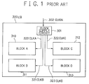
- Fig. 1 shows a schematic block diagram of a large scale integrated circuit (LSIC) including a clock signal supply circuit described in the article above.
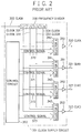
- Fig. 2 is a block diagram showing in detail the clock signal supply circuit.
- LSIC large scale integrated circuit
- the large scale integrated circuit 300 and the clock supply circuit 301 includes such constituent components as a clock input signal CLKIN 302, a block A 310, a block B 311, a block C 312, a block D 313, a clock signal A (CLKA) 320, clock signal B (CLKB) 321, a clock signal C (CLKC) 322, a clock signal D (CLKD) 323, a frequency divider circuit 330, clock signals 331 to 334, a selector A 340, a selector B 341, a selector C 342, a selector D 343, buffer circuits 350 to 353, a control circuit 360, and control signals 370 to 373.
- CLKA clock signal A
- CLKB clock signal B
- CLKC clock signal C
- CLKD clock signal D
- the LSIC 300 of Fig. 1 includes a clock supply circuit 301 and functional blocks A 310, B 311, C 312, and D 313.
- the circuit 301 receives the CLKIN signal 302 as an input signal thereto to produce clock signals including CLKA 320, CLKB 321, CLKC 322, and CLKD 323, which are connected to the blocks B 311, C 312, and D 313, respectively.
- the clock supply circuit 301 of Fig, 2 includes a frequency divider circuit 330, selector circuits 340 to 343, and buffer circuits 350 to 353.
- the divider 330 is connected to the CLKIN signal 302 as an input thereto and generates clock signals 331 to 334 by dividing the frequency of the CLKIN signal 302.
- the obtained signals 331 to 334 are linked to the selectors 340 to 343.
- the controller 360 delivers the control signals 370 to 373 respectively to the selectors 340 to 343 respectively associated therewith.
- the selectors 340 to 343 feed the respective output signals to the buffers 350 to 353. Outputs from the buffers 350 to 353 are respectively coupled with the signals CLKA 320, CLKB 321, CLKC 322, and CLKD 323, respectively.
- controller 360 receives data and address buses and control signals from the CPU and the like, not specifically shown, to conduct selection and control operations for the selectors 340 to 343 and the divided clock pulses 331 to 334.
- the functional blocks 310 to 313 of the LSIC 300 are respectively supplied with the mutually independent clock pulses 320 to 323 from the clock supply circuit 301.
- the functional blocks operate such that a signal of f MHz is fed to block A, a signal of f/4 MHz is delivered to block B, no signal is supplied to block C and a signal of f/8 MHz is sent to block D.
- the selectors 340 to 343 respectively output the predetermined clock signals respectively via the buffers 350 to 353 to the CLKA 320 to CLKD 323.
- the power consumed in the circuit is lowered when compared with a case in which the signals supplied to the functional blocks 310 to 313 are substantially equal to each other.
- the functional blocks 310 have the same load capacity.
- the ratio of the power consumption P of the circuit when the the respective blocks receive the same clock signal (same clock signal) to that of the circuit when the blocks receive the clock signals respectively having different frequencies (individual clock signal) is represented as follows.
- the power consumption can be lowered to about one third.
- the overall allowed power consumption can be arbitrarily distributed to the respective functional blocks.
- the power consumption in the case in which the same clock signals are supplied to the blocks is the maximum power consumption.
- the frequency f (MHz) of CLKIN 302 can be increased to about three times that of the associated original value. For example, if the performance of block A 310 is directly related to the frequency as in a central processing unit (CPU), the resultant performance can be multiplied by three with the same power consumption.
- Fig. 3 is a signal timing chart of clock signals produced from the frequency divider 300.
- the signals shown in Fig. 3 are supplied to the respective blocks of the circuit, these clock signals are simultaneously changed at points A, B, and C.
- the transient current in the switching operation is the same as that appearing when the CLKIN signal 302 is delivered to the blocks regardless of the clock frequencies supplied from the frequency divider 330. Namely, the transient current depends on the overall size of the LSIC 300.
- Fig. 4 is a circuit diagram showing a model of a VDD line provided in a general LSI chip.
- This circuit includes a drain power source (VDD) 91, inductance (L) 92, resistance (R) 93, a drain power source input (VDDint) 94, and a current (i) 95.
- VDD drain power source
- L inductance
- R resistance
- VDDint drain power source input
- i current
- the drain power source VDD is supplied via metal wirings to respective transistors.
- the VDD line is primarily associated with an inductance component L due to wire bondings and a resistance component R resultant from the wirings.
- VDDint VDD - [L ⁇ di(t)/dt + i(t) ⁇ R]
- GNDint [L(
- Expressions (2) and (3) indicate that the greater the transient current is or the greater the change in the transient current per unitary time is, the larger the potential deviation of VDD and GND is.
- the average or mean power consumption of the overall LSI chip can be controlled by distributing clock signals having mutually different frequencies to the respective functional blocks.
- considerations have not been particularly given to the fluctuation of the power source potential in the transient state and to the transient current, which consequently leads to drawbacks as follows.
- the average power consumption is reduced, there occurs a wrong operation due to variation in the power source potential or the circuit size is limited due to influence of the radiation noise from the power source line in association with the transient current.
- the operating voltage of power source has a decreasing tendency because of the finer machining technology of circuits thanks to the recent development of process technologies and requirements in the market. In consequence, when it is assumed that the variation in the power source potential is kept unchanged, the ratio of the variation to the operating power source potential becomes larger. This resultantly causes the wrong operation and hence restricts the circuit size.
- a large scale integrated circuit including a plurality of functional blocks coupled with each other via an address bus, a data bus, and a plurality of control signals, at least one of the functional blocks being a control block for generating and outputting the control signals therefrom.
- the control block includes means for conducting a data accessing operation to the other one of the functional blocks via the address and data buses.
- the LSIC further includes clock supply means for supplying the respectively functional blocks with a plurality of kinds of clock signals respectively corresponding to functions respectively of the functional blocks.
- the clock supply means includes a clock distributor circuit for distributing clock signals in which at least one of the clock signals has a phase different from those of the remaining clock signals and the clock signals do not conduct a setting operation at the same time.
- the clock supply means desirably includes a clock distributor circuit for distributing clock signals in which at least one of the clock signals has a clock cycle different from those of the remaining clock signals, at least one of the clock signals has a phase different from those of the remaining clock signals, and the clock signals do not conduct a setting operation at the same time.
- the clock distributor circuit of the clock supply means includes two buffer circuits, two logical product circuits including a first logical product circuit and a second logical product circuit, and one flip-flop circuit.
- the flip-flop circuit includes a clock input terminal linked with a clock input signal.
- the flip-flop circuit includes a data output terminal connected to one of the input terminals of the first logical product circuit.
- the flip-flop circuit includes an inverted data output terminal coupled with one of the input terminals of the second logical product circuit and a data input terminal of the flip-flop circuit.
- Each of the first and second logical product circuits includes other input terminal connected to the clock input signal.
- the clock input signal and output terminals respectively of the first and second logical product circuits are coupled via the buffer circuits to a predetermined functional block of the LSIC.
- the LSIC of the present invention includes independent clock supply means for supplying a plurality of kinds of clock signals corresponding to respective functions of the functional blocks.
- the clock supply means includes a clock distributor circuit distributing a plurality of output clock signals in which at least one output clock signal selected from the plural clock signals produced therefrom has a phase different from those of the remaining clock signals, and it is inhibited that all clock signals conduct the setting operation at the same time. As a result, the maximum transient current appearing in relation to the simultaneous setting operation of the clock signals is reduced.
- the clock supply means includes a clock distributor circuit distributing a plurality of output clock signals in which at least one output clock signal selected from the plural clock signals produced therefrom has a clock cycle or period different from those of the remaining clock signals and at least one output clock signal selected from the plural clock signals produced therefrom has a phase different from those of the remaining clock signals, and it is inhibited that all clock signals conduct the setting operation at the same time. Resultantly, the power consumption related to the setting operation can be minimized.
- the clock distributor circuit can be easily configured by combining two buffers, two logical product circuits, and one flip-flop circuit with each other.
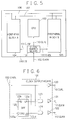
- Fig. 5 shows in a block diagram the configuration of an LSIC including an embodiment of clock signal supply means in accordance with the present invention.
- Fig. 6 is a circuit diagram showing an example of the clock supply means of Fig. 5, whereas Fig. 7 is a timing chart of clock signals supplied from the clock supply means of Fig. 6.
- LSIC large scale integrated circuit
- clock supply means 101 a clock input signal (CLKIN) 102, a CPU 103, a peripheral block A 104, a peripheral block B 105, an address/data bus 106, an interface control signal 107, a clock output signal L (CLKL) 110, a clock output signal M (CLKM) 111, a clock output signal N (CLKN) 112, buffer circuits 120 to 122, logical product (AND) circuits 123 and 124, a flip-flop (DFF) circuit 125, a clock input (CKB) terminal 125a, a data input (D) terminal 125b, a data output (Q) terminal 125c, and an inverted data output (QB) terminal 125d.
- LSIC large scale integrated circuit
- DFF flip-flop
- the LSIC 100 includes the clock supply means 101, the CPU 103, and functional blocks, namely, a peripheral block A 104 and a peripheral block B 105.
- the clock supply means 101 is connected to the CLKIN 102, CLKL 110, CLKM 111, and CLKN 112.
- the CPU 103 is linked with the CLK 110 and the peripheral blocks A 104 and B 105 are respectively coupled with the ClKM 111 and the CLKN 112.
- the CPU 103 and the peripheral blocks 104 and 105 are connected to each other via the address/data bus 106 and the interface control signal 107.
- the clock supply means 101 includes the buffer circuits 120 to 122, the AND circuits 123 and 124, and the flip-flop (DFF) circuit 125.
- the DFF circuit 125 includes the clock input (CKB) terminal 125a, the data input (D) terminal 125b, the data output (Q) terminal 125c, and the inverted data output (QB) terminal 125d.
- the CKB terminal 125a is linked with the clock input (CLKIN) signal 102, whereas the D terminal 125b is coupled with an output signal from the QB terminal 125d.
- the Q terminal 125c outputs a signal fed to one of the input terminals of the AND circuit 123
- the QB terminal 125d delivers a signal to be inputted to one of the input terminals of the AND circuit 124.
- the remaining input terminals of the AND circuits 123 and 124 are connected to the CLKIN signal 102.
- the buffers 120 to 122 respectively receive as input signals thereto the CLKIN signal 102, an output signal from the AND circuit 123, and an output from the AND circuit 124.
- the buffers 120 to 122 respectively include output terminals connected to the CLKL, CLKM, and CLKN signals 111 to 112, respectively.
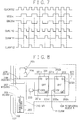
- Fig. 7 shows an operation timing chart of the clock supply means including a combination of the flip-flop circuit and the AND circuits.
- the CLKM signal 111 and the CLKN 112 have mutually different phases of pulses and only two kinds of clock signals selected from the three kinds of clock signals CLKL 110, CLKM 111, and CLKN 112 are related to timing of simultaneous change. This makes it possible to suppress the transient current which influences the width of deviation in the power source potential as well as the increase in the radiation noise from the power source line.
- the maximum transient current can be decreased to about 2/3 that appearing when the clock signals supplied to these blocks are changed at the same time.
- the circuit size can be increased to about 1.5 that of the conventional circuit.
- the pulse waveform of clock signal CLKL 110 is substantially equal to that of CLKIN 102.
- the pulse width of CLKM 111 is the sane as that of CLKIN 102
- the pulse cycle of CLKM 111 is twice that of CLKIN 102.
- the signals CLKN 112 and CLKM 111 have the same pulse waveform with a phase difference of 1/2 cycle therebetween. Consequently, in a block supplied with CLKM 111 and CLKN 112, the number of setting operations as well as the power consumption are reduced to those of the operation with clock signals having the pulse waveform of CLKIN 102.
- the pulse cycle may be doubled.
- the characteristic of the clock pulses conforms to the contents of the pertinent functional block, it is possible to much more decrease the power consumption.
- the transient current can be suppressed by altering the phase between the clock pulses.
- the clock pulses having mutually different pulse cycles are simultaneously fed to the respective blocks, the mean power consumption and the cost performance of the LSI chip are improved when compared with the case in which the respective blocks are supplied with uniform clock pulses as described in relation to the prior art example.
- Fig. 8 shows in a block diagram the configuration of an interface circuit of the peripheral block A 104 to provide an interface with respect to the CPU 103.
- the configuration includes the peripheral block A 104, the address/data bus 106, the interface control signal 107, the CLKM signal 111, an address latch/decoder 200, flip-flop (DFF) circuits 201 and 202, a clock input (CKB) terminal 201a, a CK terminal 202a, data input (D) terminals 201b and 202b, data output (Q) terminals 201c and 202c, inverted data output (QB) terminals 201d and 202d, logical product (AND) terminals 203 and 204, a three-state buffer circuit 205, an address control (ASTRV) signal 206, a write control (WRSTRV) signal 207, a read control (RDSTRV) signal 208, a bit line data (DATA) signal 209, an address decode (
- ASTRV address control
- the interface circuit of Fig. 8 includes the address latch/decoder 200, the DFF circuits 201 and 202, the AND circuits 203 and 204, and the three-state buffer 205.
- the address latch/decoder 200 is linked with the address/data bus 106 and the ASTRV signal 206. This circuit 200 latches therein a value of the address/data bus 106 at timing of the falling edge of the ASTRV signal 206, decodes the value, and then produces an address decode (SEL) signal 210 as a result of the decoding operation.
- the SEL signal 210 is coupled with one of the inputs of the AND circuit 203.
- the AND circuit 203 Linked with the remaining input of the AND circuit 203 is the WRSTRV signal 207 which belongs to the interface control signal 107 and which controls the write operation.
- the SEL signal 210 is connected to one of the inputs of the AND circuit 204, whereas the RDSTRV signal 208 belonging to the interface control signal 107 and supervising the read operation is linked with the remaining input of the AND circuit 204.
- the AND circuit 203 produces an output to be fed to the CKB terminal of the DFF circuit 201, the data signal 209 on a predetermined bit line of the address/data bus 106 is connected to the D terminal of the DFF circuit 201.
- the CLKM signal 111 is coupled with the CK terminal 202a of the DFF circuit 202, whereas the output from the Q terminal 201 of the DFF circuit 201 is linked with the D terminal of the DFF circuit 201.
- the Q terminal 202c of the DFF circuit 202 delivers a control signal, i.e., BIT 211 for the peripheral block A 104 and is connected to an input port of the three-state buffer 205.
- the buffer 205 creates an output signal to be linked with a predetermined bit line data (DATA) signal 209 of the address/data bus 106.
- DATA bit line data
- Figs. 9A and 9B are signal timing charts showing operation of the interface for the peripheral block of Fig. 5.
- Figs. 9A and 9B are related to the write and read operations, respectively. Shown in these charts are accesses at different points of timing with respect to the CKLM signal 111 in the write and read operations. As can be seen from these timing charts, the interface is appropriately established for the peripheral block.
- the power consumption as well as the noise can be reduced without increasing the circuit size of the LSIC.
Landscapes
- Engineering & Computer Science (AREA)
- Theoretical Computer Science (AREA)
- Physics & Mathematics (AREA)
- General Engineering & Computer Science (AREA)
- General Physics & Mathematics (AREA)
- Logic Circuits (AREA)
- Semiconductor Integrated Circuits (AREA)
- Power Sources (AREA)
- Microcomputers (AREA)
Applications Claiming Priority (3)
| Application Number | Priority Date | Filing Date | Title |
|---|---|---|---|
| JP217304/96 | 1996-08-19 | ||
| JP21730496 | 1996-08-19 | ||
| JP8217304A JP2959482B2 (ja) | 1996-08-19 | 1996-08-19 | 大規模集積回路 |
Publications (2)
| Publication Number | Publication Date |
|---|---|
| EP0825513A2 true EP0825513A2 (de) | 1998-02-25 |
| EP0825513A3 EP0825513A3 (de) | 2005-07-20 |
Family
ID=16702056
Family Applications (1)
| Application Number | Title | Priority Date | Filing Date |
|---|---|---|---|
| EP97113999A Withdrawn EP0825513A3 (de) | 1996-08-19 | 1997-08-13 | Taktverteilung in einer LSI-Schaltung |
Country Status (3)
| Country | Link |
|---|---|
| US (1) | US5963075A (de) |
| EP (1) | EP0825513A3 (de) |
| JP (1) | JP2959482B2 (de) |
Cited By (1)
| Publication number | Priority date | Publication date | Assignee | Title |
|---|---|---|---|---|
| EP0953892A1 (de) * | 1998-04-29 | 1999-11-03 | Lsi Logic Corporation | Verfahren zur Versorgung von Lastkreisen mit Taktsignalen in einer ASIC-Vorrichtung |
Families Citing this family (50)
| Publication number | Priority date | Publication date | Assignee | Title |
|---|---|---|---|---|
| FR2773020B1 (fr) * | 1997-12-24 | 2000-03-10 | Sgs Thomson Microelectronics | Circuit de distribution d'horloge dans un circuit integre |
| US6472922B1 (en) * | 1999-01-14 | 2002-10-29 | Sony Corporation | System and method for flexibly distributing timing signals |
| US6529054B1 (en) * | 1999-02-12 | 2003-03-04 | Infineon Technologies Ag | Prefetch architectures for data and time signals in an integrated circuit and methods therefor |
| US6578155B1 (en) * | 2000-03-16 | 2003-06-10 | International Business Machines Corporation | Data processing system with adjustable clocks for partitioned synchronous interfaces |
| US7023257B1 (en) * | 2000-10-26 | 2006-04-04 | Cypress Semiconductor Corp. | Architecture for synchronizing and resetting clock signals supplied to multiple programmable analog blocks |
| US7765095B1 (en) | 2000-10-26 | 2010-07-27 | Cypress Semiconductor Corporation | Conditional branching in an in-circuit emulation system |
| US6724220B1 (en) | 2000-10-26 | 2004-04-20 | Cyress Semiconductor Corporation | Programmable microcontroller architecture (mixed analog/digital) |
| US8103496B1 (en) | 2000-10-26 | 2012-01-24 | Cypress Semicondutor Corporation | Breakpoint control in an in-circuit emulation system |
| US8176296B2 (en) | 2000-10-26 | 2012-05-08 | Cypress Semiconductor Corporation | Programmable microcontroller architecture |
| US8160864B1 (en) | 2000-10-26 | 2012-04-17 | Cypress Semiconductor Corporation | In-circuit emulator and pod synchronized boot |
| US8149048B1 (en) | 2000-10-26 | 2012-04-03 | Cypress Semiconductor Corporation | Apparatus and method for programmable power management in a programmable analog circuit block |
| JP3880310B2 (ja) * | 2000-12-01 | 2007-02-14 | シャープ株式会社 | 半導体集積回路 |
| US7406674B1 (en) | 2001-10-24 | 2008-07-29 | Cypress Semiconductor Corporation | Method and apparatus for generating microcontroller configuration information |
| US8078970B1 (en) | 2001-11-09 | 2011-12-13 | Cypress Semiconductor Corporation | Graphical user interface with user-selectable list-box |
| US8042093B1 (en) | 2001-11-15 | 2011-10-18 | Cypress Semiconductor Corporation | System providing automatic source code generation for personalization and parameterization of user modules |
| US7844437B1 (en) | 2001-11-19 | 2010-11-30 | Cypress Semiconductor Corporation | System and method for performing next placements and pruning of disallowed placements for programming an integrated circuit |
| US8069405B1 (en) | 2001-11-19 | 2011-11-29 | Cypress Semiconductor Corporation | User interface for efficiently browsing an electronic document using data-driven tabs |
| US6971004B1 (en) | 2001-11-19 | 2005-11-29 | Cypress Semiconductor Corp. | System and method of dynamically reconfiguring a programmable integrated circuit |
| US7774190B1 (en) | 2001-11-19 | 2010-08-10 | Cypress Semiconductor Corporation | Sleep and stall in an in-circuit emulation system |
| US7770113B1 (en) | 2001-11-19 | 2010-08-03 | Cypress Semiconductor Corporation | System and method for dynamically generating a configuration datasheet |
| US8103497B1 (en) | 2002-03-28 | 2012-01-24 | Cypress Semiconductor Corporation | External interface for event architecture |
| US7308608B1 (en) | 2002-05-01 | 2007-12-11 | Cypress Semiconductor Corporation | Reconfigurable testing system and method |
| JP2004046995A (ja) * | 2002-07-15 | 2004-02-12 | Hitachi Ltd | ディスク装置、及びこれを用いたディスクシステム |
| US7761845B1 (en) | 2002-09-09 | 2010-07-20 | Cypress Semiconductor Corporation | Method for parameterizing a user module |
| JP4165180B2 (ja) * | 2002-10-22 | 2008-10-15 | 松下電器産業株式会社 | 半導体集積回路 |
| US7474137B2 (en) * | 2003-12-19 | 2009-01-06 | Nxp B.V. | Integrated circuit clock distribution |
| US7295049B1 (en) | 2004-03-25 | 2007-11-13 | Cypress Semiconductor Corporation | Method and circuit for rapid alignment of signals |
| US8069436B2 (en) | 2004-08-13 | 2011-11-29 | Cypress Semiconductor Corporation | Providing hardware independence to automate code generation of processing device firmware |
| US8286125B2 (en) | 2004-08-13 | 2012-10-09 | Cypress Semiconductor Corporation | Model for a hardware device-independent method of defining embedded firmware for programmable systems |
| US7332976B1 (en) | 2005-02-04 | 2008-02-19 | Cypress Semiconductor Corporation | Poly-phase frequency synthesis oscillator |
| US7400183B1 (en) | 2005-05-05 | 2008-07-15 | Cypress Semiconductor Corporation | Voltage controlled oscillator delay cell and method |
| US8089461B2 (en) | 2005-06-23 | 2012-01-03 | Cypress Semiconductor Corporation | Touch wake for electronic devices |
| US8085067B1 (en) | 2005-12-21 | 2011-12-27 | Cypress Semiconductor Corporation | Differential-to-single ended signal converter circuit and method |
| US8067948B2 (en) | 2006-03-27 | 2011-11-29 | Cypress Semiconductor Corporation | Input/output multiplexer bus |
| US20080046772A1 (en) * | 2006-07-17 | 2008-02-21 | International Business Machines Corporation | Shifting inactive clock edge for noise reduction |
| US9564902B2 (en) | 2007-04-17 | 2017-02-07 | Cypress Semiconductor Corporation | Dynamically configurable and re-configurable data path |
| US8092083B2 (en) | 2007-04-17 | 2012-01-10 | Cypress Semiconductor Corporation | Temperature sensor with digital bandgap |
| US8130025B2 (en) | 2007-04-17 | 2012-03-06 | Cypress Semiconductor Corporation | Numerical band gap |
| US7737724B2 (en) | 2007-04-17 | 2010-06-15 | Cypress Semiconductor Corporation | Universal digital block interconnection and channel routing |
| US8516025B2 (en) | 2007-04-17 | 2013-08-20 | Cypress Semiconductor Corporation | Clock driven dynamic datapath chaining |
| US8040266B2 (en) | 2007-04-17 | 2011-10-18 | Cypress Semiconductor Corporation | Programmable sigma-delta analog-to-digital converter |
| US8026739B2 (en) | 2007-04-17 | 2011-09-27 | Cypress Semiconductor Corporation | System level interconnect with programmable switching |
| US9720805B1 (en) | 2007-04-25 | 2017-08-01 | Cypress Semiconductor Corporation | System and method for controlling a target device |
| US8266575B1 (en) | 2007-04-25 | 2012-09-11 | Cypress Semiconductor Corporation | Systems and methods for dynamically reconfiguring a programmable system on a chip |
| US8065653B1 (en) | 2007-04-25 | 2011-11-22 | Cypress Semiconductor Corporation | Configuration of programmable IC design elements |
| US8049569B1 (en) | 2007-09-05 | 2011-11-01 | Cypress Semiconductor Corporation | Circuit and method for improving the accuracy of a crystal-less oscillator having dual-frequency modes |
| US20090102529A1 (en) * | 2007-10-23 | 2009-04-23 | International Business Machines Corporation | Shifting inactive clock edge for noise reduction |
| US9448964B2 (en) | 2009-05-04 | 2016-09-20 | Cypress Semiconductor Corporation | Autonomous control in a programmable system |
| JP2012195689A (ja) | 2011-03-15 | 2012-10-11 | Toshiba Corp | 半導体集積回路 |
| CN113615088B (zh) * | 2019-03-26 | 2023-07-14 | 华为技术有限公司 | 跨时钟域同步电路以及方法 |
Citations (2)
| Publication number | Priority date | Publication date | Assignee | Title |
|---|---|---|---|---|
| JPH0514157A (ja) * | 1991-07-02 | 1993-01-22 | Mitsubishi Electric Corp | 半導体集積回路 |
| US5627795A (en) * | 1994-04-08 | 1997-05-06 | Kabushiki Kaisha Toshiba | Timing generating device |
Family Cites Families (8)
| Publication number | Priority date | Publication date | Assignee | Title |
|---|---|---|---|---|
| US4164787A (en) * | 1977-11-09 | 1979-08-14 | Bell Telephone Laboratories, Incorporated | Multiple microprocessor intercommunication arrangement |
| US4745573A (en) * | 1986-04-11 | 1988-05-17 | Symbolics Inc. | Programmable clock generator |
| JPS63104443A (ja) * | 1986-10-22 | 1988-05-09 | Hitachi Ltd | 大規模集積回路 |
| US5164619A (en) * | 1990-11-21 | 1992-11-17 | Hewlett-Packard Company | Low skew clocking system for VLSI integrated circuits |
| US5317601A (en) * | 1992-08-21 | 1994-05-31 | Silicon Graphics | Clock distribution system for an integrated circuit device |
| US5471607A (en) * | 1993-04-22 | 1995-11-28 | Analog Devices, Inc. | Multi-phase multi-access pipeline memory system |
| US5394443A (en) * | 1993-12-23 | 1995-02-28 | Unisys Corporation | Multiple interval single phase clock |
| US5774001A (en) * | 1995-12-20 | 1998-06-30 | Intel Corporation | Method for eliminating multiple output switching timing skews in a source synchronous design |
-
1996
- 1996-08-19 JP JP8217304A patent/JP2959482B2/ja not_active Expired - Fee Related
-
1997
- 1997-08-13 EP EP97113999A patent/EP0825513A3/de not_active Withdrawn
- 1997-08-19 US US08/914,091 patent/US5963075A/en not_active Expired - Lifetime
Patent Citations (2)
| Publication number | Priority date | Publication date | Assignee | Title |
|---|---|---|---|---|
| JPH0514157A (ja) * | 1991-07-02 | 1993-01-22 | Mitsubishi Electric Corp | 半導体集積回路 |
| US5627795A (en) * | 1994-04-08 | 1997-05-06 | Kabushiki Kaisha Toshiba | Timing generating device |
Cited By (2)
| Publication number | Priority date | Publication date | Assignee | Title |
|---|---|---|---|---|
| EP0953892A1 (de) * | 1998-04-29 | 1999-11-03 | Lsi Logic Corporation | Verfahren zur Versorgung von Lastkreisen mit Taktsignalen in einer ASIC-Vorrichtung |
| US6313683B1 (en) | 1998-04-29 | 2001-11-06 | Lsi Logic Corporation | Method of providing clock signals to load circuits in an ASIC device |
Also Published As
| Publication number | Publication date |
|---|---|
| JPH1063368A (ja) | 1998-03-06 |
| EP0825513A3 (de) | 2005-07-20 |
| JP2959482B2 (ja) | 1999-10-06 |
| US5963075A (en) | 1999-10-05 |
Similar Documents
| Publication | Publication Date | Title |
|---|---|---|
| US5963075A (en) | Large scale integrated circuit having functional blocks controlled with clock signals that conduct setting operations at different times | |
| US5506982A (en) | Data processing system generating clock signal from an input clock, phase locked to the input clock and used for clocking logic devices | |
| US6744289B2 (en) | Clock divider circuit with duty cycle correction and minimal additional delay | |
| US5336939A (en) | Stable internal clock generation for an integrated circuit | |
| US5914996A (en) | Multiple clock frequency divider with fifty percent duty cycle output | |
| US5915107A (en) | Cross clock domain clocking for a system using two clock frequencies where one frequency is fractional multiple of the other | |
| JP3732556B2 (ja) | クロック供給回路 | |
| US7245168B2 (en) | Clock selection circuit and digital processing system for reducing glitches | |
| US6985041B2 (en) | Clock generating circuit and method | |
| JP2002182777A (ja) | クロック切り換え回路 | |
| JPH11145786A (ja) | フリップフロップのリセット回路 | |
| JP4119017B2 (ja) | 半導体装置 | |
| JPH06204858A (ja) | 高周波プログラム可能分周器 | |
| EP4116794A1 (de) | Spannungsregelungsschaltung und -verfahren, betriebssystem und integriertes modul und schaltung | |
| US6552958B2 (en) | Semiconductor integrated circuit device | |
| US5850154A (en) | Data transmission method and data transmission circuit | |
| US6092129A (en) | Method and apparatus for communicating signals between circuits operating at different frequencies | |
| US7443222B1 (en) | Dynamic clock control | |
| CN118017998B (zh) | 一种无毛刺零延时的分频时钟切换电路 | |
| KR950008955B1 (ko) | 클럭 분배 회로 | |
| KR100261868B1 (ko) | 주파수 분주 장치 | |
| EP0530712A1 (de) | Vielfach gekateter Prozessor und Betriebsverfahren dafür | |
| JP2924023B2 (ja) | クロック分周回路 | |
| WO2006018801A1 (en) | Mixed signal integrated circuit | |
| JP3667461B2 (ja) | パルス生成回路およびそれを搭載した半導体集積回路装置 |
Legal Events
| Date | Code | Title | Description |
|---|---|---|---|
| PUAI | Public reference made under article 153(3) epc to a published international application that has entered the european phase |
Free format text: ORIGINAL CODE: 0009012 |
|
| AK | Designated contracting states |
Kind code of ref document: A2 Designated state(s): AT BE CH DE DK ES FI FR GB GR IE IT LI LU MC NL PT SE |
|
| AX | Request for extension of the european patent |
Free format text: AL;LT;LV;RO;SI |
|
| RAP1 | Party data changed (applicant data changed or rights of an application transferred) |
Owner name: NEC ELECTRONICS CORPORATION |
|
| PUAL | Search report despatched |
Free format text: ORIGINAL CODE: 0009013 |
|
| AK | Designated contracting states |
Kind code of ref document: A3 Designated state(s): AT BE CH DE DK ES FI FR GB GR IE IT LI LU MC NL PT SE |
|
| AX | Request for extension of the european patent |
Extension state: AL LT LV RO SI |
|
| 17P | Request for examination filed |
Effective date: 20050607 |
|
| AKX | Designation fees paid |
Designated state(s): DE FR GB |
|
| 17Q | First examination report despatched |
Effective date: 20050930 |
|
| STAA | Information on the status of an ep patent application or granted ep patent |
Free format text: STATUS: THE APPLICATION HAS BEEN WITHDRAWN |
|
| 18W | Application withdrawn |
Effective date: 20070312 |