EP0823075B1 - Verringerung von restpotential und geisterbildformung in einem photoleiter - Google Patents
Verringerung von restpotential und geisterbildformung in einem photoleiter Download PDFInfo
- Publication number
- EP0823075B1 EP0823075B1 EP96908692A EP96908692A EP0823075B1 EP 0823075 B1 EP0823075 B1 EP 0823075B1 EP 96908692 A EP96908692 A EP 96908692A EP 96908692 A EP96908692 A EP 96908692A EP 0823075 B1 EP0823075 B1 EP 0823075B1
- Authority
- EP
- European Patent Office
- Prior art keywords
- photoconductor
- charge
- conditioning
- radiation
- exposing
- Prior art date
- Legal status (The legal status is an assumption and is not a legal conclusion. Google has not performed a legal analysis and makes no representation as to the accuracy of the status listed.)
- Expired - Lifetime
Links
Images



Classifications
-
- G—PHYSICS
- G03—PHOTOGRAPHY; CINEMATOGRAPHY; ANALOGOUS TECHNIQUES USING WAVES OTHER THAN OPTICAL WAVES; ELECTROGRAPHY; HOLOGRAPHY
- G03G—ELECTROGRAPHY; ELECTROPHOTOGRAPHY; MAGNETOGRAPHY
- G03G21/00—Arrangements not provided for by groups G03G13/00 - G03G19/00, e.g. cleaning, elimination of residual charge
- G03G21/0094—Arrangements not provided for by groups G03G13/00 - G03G19/00, e.g. cleaning, elimination of residual charge fatigue treatment of the photoconductor
-
- G—PHYSICS
- G03—PHOTOGRAPHY; CINEMATOGRAPHY; ANALOGOUS TECHNIQUES USING WAVES OTHER THAN OPTICAL WAVES; ELECTROGRAPHY; HOLOGRAPHY
- G03G—ELECTROGRAPHY; ELECTROPHOTOGRAPHY; MAGNETOGRAPHY
- G03G21/00—Arrangements not provided for by groups G03G13/00 - G03G19/00, e.g. cleaning, elimination of residual charge
Definitions
- the present invention relates to electrophotographic imaging and, more particularly, to techniques for reducing residual potential and ghosting in a photoconductor.
- An electrophotographic imaging process involves the steps of applying a uniform surface charge to a photoconductor, and exposing the photoconductor to imaging radiation that discharges the photoconductor in selected areas to define a latent electrostatic image.
- the latent image is then developed by the deposition of a dry or liquid toner on the photoconductor surface.
- the toner electrostatically adheres to the imaged areas of the photoconductor to form a developed image that is transferred to an imaging substrate.
- the optical density of the deposited toner, and of the image transferred to the imaging substrate is a function of the potential difference, or "contrast,” between imaged and unimaged areas of the photoconductor.
- the degree of contrast depends on the difference between the surface charge potential initially applied to the photoconductor and the potential of the imaged areas after discharge.
- the difference between the surface charge potential and the discharged potential in the imaged areas should be as high as possible.
- the discharge process does not immediately reduce the surface charge potential to zero, but rather produces a residual electrostatic potential that limits the degree of contrast that can be achieved.
- the existence of the residual potential can be explained by examining the mechanics of the discharge process, which has two components: an initial, rapid discharge phase and a subsequent, gradual discharge phase.
- the imaging radiation generates charge carriers that quickly neutralize the surface charge in imaged areas to lower the surface potential.
- a portion of the charge carriers becomes trapped within the photoconductor bulk, resulting in the maintenance of a residual potential in the imaged areas.
- residual potential can also contribute to the appearance of undesirable "ghost" images in previously imaged areas of the photoconductor.
- a ghost image is any visible remnant of a previous image superimposed on a present image.
- the ghosting problem can result from a variety of mechanisms.
- One mechanism is the accumulation of trapped charge carriers in discharged areas over a series of imaging cycles that results in a "build-up" of residual electrostatic potential.
- the accumulation of trapped charge carriers leads to a higher residual potential in previously imaged areas of the photoconductor relative to previously unimaged areas.
- the accumulation of trapped charge carriers may also create space charge fields that decrease conductivity in the previously imaged areas.
- the presence of higher residual potentials and/or space charge fields acts as a nonuniformity that decreases optical density upon development, and produces ghost images in areas in which differences in residual potential or conductivity exist.
- the erase lamp treats the undesirable nonuniformities caused by residual potential and ghosting by illuminating the entire photoconductor with radiation having wavelengths selected to be near the absorption peak of the particular photoconductive material used.
- the erase lamp is positioned adjacent the photoconductor between the development stage and the charging stage of the electrophotographic system.
- the erase lamp generates charge carriers that flood the photoconductor, discharging any remaining surface charge and, in theory, erasing the previous latent image. In reality, however, the charge carriers generated by the erase lamp merely populate trap sites within the photoconductor in a uniform manner.
- the use of an erase lamp has not been completely effective in eliminating ghost images and does not reduce residual potential.
- the uniform illumination by the erase lamp does not necessarily result in uniform preparation of the photoconductor for the next charge-expose cycle. Even if the undischarged surface potential is made uniform, residual potentials still may exist due to the presence of trapped carriers in the photoconductor bulk. Further, the uniform erase technique may actually result in an added accumulation of the newly-generated charge carriers in trap sites, thereby aggravating the residual potential problem already present over successive cycles.
- the unimaged areas of the photoconductor maintain a high surface potential that supports an electric field. The electric field is helpful to some degree in sweeping away the charge carriers generated by the erase lamp before they can become trapped.
- an erase lamp may help to stabilize the residual potential in nonimaged areas over repeated cycling.
- the existing field is too weak to sweep away the newly-generated charge carriers.
- the charge carriers are trapped in the imaged areas, creating added residual potential relative to nonimaged areas.
- the added residual potential can both reduce optical density and contribute to ghosting over a number of cycles.
- the erase lamp technique also fails to eliminate internal space-charge fields in the photoconductor bulk.
- the developed optical density not only depends on the difference in surface potentials between imaged and unimaged areas of the photoconductor, which determines the maximum development bias potential that can be applied, but also varies as a function of the effective electrical impedance of the photoconductor during development. Trapped charge carriers can create space charge fields that are not measurable by the surface potential, but which nevertheless adversely affect the impedance of the photoconductor in imaged areas.
- the effective impedance in the imaged areas limits the amount of toner than can be deposited during development, producing visible ghosting problems.
- US-A-4 413 837 discloses an electrostatic copying apparatus comprising a photosensitive drum.
- an electrifying device for electrifying the photosensitive layer to render it photoconductive; an optical device for emitting light beams on the photosensitive layer to produce thereon a static latent image; a developing device for developing the static latent image by a toner; a transcription device for transcribing a developed image on a copy sheet; a peeling device for removing a copy sheet on which a toner image has been described from the surface of the photosensitive drum; a cleaning device for taking off a toner remaining on the surface of the photosensitive layer; and a discharge device for expelling electric energy charged on the surface of the photosensitive layer.
- Said discharge device comprises a light source for emitting light having a long wave length for releasing trapped charges in the photosensitive layer. All the above members are arranged in the order mentioned around the photosensitive drum.
- the present invention is directed to a system and method that alleviate the problems of low optical density and ghosting by reducing residual electrostatic potential in a photoconductor.
- the system and method of the present invention apply a charge to a surface of the photoconductor, and expose the photoconductor to conditioning radiation having wavelengths selected to release charge carriers from trap sites distributed within the photoconductor.
- the applied charge establishes an electric field across the photoconductor.
- the released charge carriers are transported within the photoconductor under influence of the electric field to reduce residual electrostatic potential in the photoconductor.
- the system and method of the present invention can be applied to both positively and negatively charging photoconductors.
- the system and method of the present invention also can be applied to existing electrophotography machines, and can be realized, at least in part, by adaptation of existing hardware present in such machines, thereby adding very little complexity, cost, size, or power consumption.
- Fig. 1 is a simplified plot of electrostatic potential over the surface of an imaged photoconductor, illustrating the problem of residual electrostatic potential.
- the plot represents the electrostatic potential in unimaged areas 10 and 12, relative to the electrostatic potential in an imaged area 14 that has been discharged by exposure to imaging radiation.
- the surface potential in the unimaged areas 10, 12 remains at a charged potential V C of, for example, six-hundred and fifty (650) volts, as established by a scorotron or other charging device.
- the surface potential in imaged area 14 should ideally drop from the charged potential V C to a discharged potential of zero.
- V R residual electrostatic potential
- the residual potential V R shown in Fig. 1 as approximately one-hundred and fifty (150) volts, undesirably limits the contrast that can be achieved between the discharge potential and a development bias potential applied during subsequent toner development of imaged area 14.
- the limited contrast results in reduced optical density in the developed image.
- Fig. 2 is a potential versus position plot similar to that shown in Fig. 1, but illustrating the added problem of ghosting due to a build-up in residual electrostatic potential V R .
- the build-up of residual potential V R occurs over a succession of imaging cycles during which trapped charge carriers accumulate within the photoconductor bulk upon discharge.
- the plot represents the electrostatic potential in nonimaged areas 10, 12 relative to imaged area 14, which has been discharged by imaging radiation.
- the plot represents the electrostatic potential in an imaged area 16 that has been subjected to a large number of previous discharge cycles relative to another imaged area 18 that has been subjected to a lesser number of previous discharge cycles.
- the surface potential of imaged area 18 has dropped to a residual potential V R .
- the ghost potential V G shown in Fig. 2 as approximately two-hundred and fifty (250) volts, not only reduces the contrast, and hence optical density, that can be achieved for toner deposition, but also creates a difference potential between imaged areas 16 and 18 that can lead to visible ghosting in the developed image.
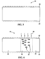
- Figs. 3-6 are schematic cross-sectional representations of a photoconductor 20, illustrating mechanisms leading to the problems of residual potential and ghosting.
- Fig. 3 shows photoconductor 20 after uniform surface charging by a scorotron or other charge means such as a roller charging device.
- the photoconductor 20 has an imaging surface 22 to which the uniform surface charge is applied. After charging, a positive charge resides on the imaging surface 22 and a negative charge resides on a ground plane surface 24 of photoconductor 20.
- Fig. 4 shows photoconductor 20 during a first stage of an image exposure operation.
- Imaging radiation 26 exposes imaging surface 22 to define unimaged areas 28 and 30, which maintain the initial surface potential, and imaged area 32, which is discharged to produce a discharge potential at imaging surface 22.
- the imaging radiation 26 creates electron-hole pairs 34 within the bulk or near surface of photoconductor 20 in imaged area 32.
- the charged potentials in unimaged areas 28 and 30 can be represented, for example, by those shown with respect to areas 10 and 12 in the plots of Figs. 1 and 2.
- the discharged potential in imaged area 32 can be represented by that shown with respect to area 14 in the plots of either Fig 1 or Fig. 2.
- a fraction of electron-note pairs 34 generated by imaging radiation 26 separate under the influence of an electric field existing between the positively-charged imaging surface 22 and the negatively-charged ground plane surface 24.
- the separated electron-hole pairs 34 produce electrons 36 and holes 38 that transport under the influence of the electric field toward imaging surface 22 and ground plane surface 24, respectively, thereby redistributing charge within photoconductor 20 to discharge the surface potential.
- holes 38 are generally more mobile than electrons 36 and transport more readily through photoconductor 20, both the holes and electrons contribute to redistribution of charge, and therefore will be generically referred to herein as "charge carriers.”
- a system and method for reducing residual electrostatic potential in a photoconductor such as photoconductor 20 of Figs 3-6.
- the system and method of the present invention apply a charge to imaging surface 22 of photoconductor 20 and expose the photoconductor to conditioning radiation having wavelengths selected to release charge carriers 36, 38 from trap sites 40 within the photoconductor.
- the applied charge establishes an electric field across photoconductor 20.
- the released charge carriers 36, 38 transport within photoconductor 20 under influence of the electric field to reduce residual electrostatic potential V R in the photoconductor.
- the electric field prevents re-trapping of the released charge carriers 36, 38 during transport by effectively sweeping them out of the bulk of photoconductor 20 to imaging surface 22 and ground plane surface 24, respectively.
- the resulting reduction in residual electrostatic potential V R increases optical density and eliminates ghosting problems in the subsequently developed image.
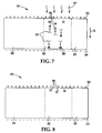
- Fig. 7 is a schematic cross-sectional representation of photoconductor 20 of Fig. 6 during application of the system and method of the present invention.
- the charge applied to imaging surface 22 produces an electric field E across the bulk of photoconductor 20.
- the conditioning radiation 42 has a wavelength selected to excite charge carriers 36, 38 out of their respective traps 40. Once released, charge carriers 36, 38 are swept out of photoconductor 20 to imaging surface 22 and ground plane surface 24, respectively, by the applied electric field E, thereby reducing the portion of the residual electrostatic potential V R attributable to trapped charge carriers.
- photoconductor 20 may retain a small amount of immobile electrons 36, but otherwise is substantially free of trapped charge carriers 36, 38 capable of generating residual potential and/or ghost images in imaged area 32.
- the conditioning radiation 42 includes wavelengths selected to release charge carriers 36, 38 held in trap sites 40, but preferably does not include wavelengths capable of discharging photoconductor 20. Wavelengths that discharge photoconductor 20 lead to generation of large numbers of new charge carriers that can flood photoconductor 20 and become trapped, compounding the problems of low optical density and ghosting. Therefore, the wavelength of conditioning radiation 42 is tuned to match known trap energies of the particular photoconductive material used. The tuned conditioning radiation 42 is selected to excite charge carriers 36, 38 out of their respective trap sites 40, but avoids significant generation of new, previously immobile charge carriers. Wavelengths overlapping the absorption band of the photoconductive material are filtered out of conditioning radiation 42, thereby suppressing discharge and the associated problems of added trapping.
- the particular wavelengths selected for conditioning radiation 42 will vary with the type of photoconductive material used. Specifically, the selected wavelengths will vary with the absorption band exhibited by the photoconductive material used.
- the effectiveness of conditioning radiation 42 in reducing residual potential V R will be a function of other parameters including the intensity of the conditioning radiation, the time that photoconductor 20 is exposed to the conditioning radiation, and the strength of the applied electric field E.
- the intensity of conditioning radiation 42 will determine the number of photons transmitted to photoconductor 20 per unit time, and hence the amount of trapped charge carriers 36, 38 released in the same unit time.
- the exposure time will determine the total number of photons transmitted by conditioning radiation 42 over the course of exposure with a given intensity, and hence the total amount of charge carriers 36, 38 released.
- the strength of the electric field E will then determine the ability of charge carriers 36, 38, once released, to transport through the bulk of photoconductor 20 to imaging surface 22 and ground plane surface 24, respectively.
- the above parameters may require adjustment for optimum results.
- conditioning radiation 42 should include wavelengths greater than the absorption band of the particular photoconductive material to avoid discharge.
- conditioning radiation 42 having wavelengths in a range of approximately one-thousand (1000) to four-thousand five-hundred (4500) nanometers will release a sufficient number of trapped charge carriers.
- Such wavelengths fall in the near infrared and infrared range, which is well beyond the above absorption band. Use of near infrared and infrared wavelengths in the above range thereby avoids significant absorption that can lead to discharge and the generation of a large number of new charge carriers.
- conditioning radiation 42 is tuned to avoid the pitfalls of broad-spectrum erase lamps. Although conditioning radiation 42 should be tuned to wavelengths greater than the absorption band of the particular photoconductive material, it is conceivable that wavelengths falling within the absorption band may be tolerated to some extent, provided that intensities are small enough to avoid a large amount of discharge. Thus, a filter passing wavelengths falling within the absorption band nevertheless may be suitable if the peak of the filter pass band falls outside of the absorption band.
- Figs. 9a-11b show embodiments 1, 3 and 4 (not covered by the present invention) and embodiment 2 (in accordance with the present invention).
- the illustrated embodiments relate to use of the system in drum- and belt-based electrophotography machines, and therefore demonstrate examples of various photoconductor structures to which the principles of the present invention may be applied.
- a charge means that applies a charge to a surface of the respective photoconductor
- a conditioning means that exposes the photoconductor to conditioning radiation having wavelengths selected to release charge carriers from trap sites within the photoconductor.
- the conditioning means can be provided by incorporating a dedicated source of conditioning radiation in the electrophotography machine.
- the charge means can be realized, however, by adaptation of hardware already present in the electrophotography machine, as will be described. The charge means thereby adds very little complexity, cost, size, or power consumption to the existing electrophotography machine.
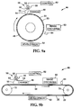
- Fig. 9a is a schematic representation of an electrophotography machine 44 incorporating a first embodiment (not covered by the present invention).
- the electrophotographic machine 44 includes a photoconductor 20 supported by a drum 46.
- the photoconductor 20 may be formed, for example, by coating a surface of drum 40 with photoconductive material, or by affixing a prefabricated photoconductor sheet or a plurality of photoconductor sheet sections to the surface of the drum.
- the drum 46 is coupled to a motor (not shown) that rotates the drum in a direction of travel during image exposure cycles.
- the electrophotographic machine 44 further includes a set of imaging hardware positioned adjacent to imaging surface 22 of photoconductor 20.
- the imaging hardware includes, in order of position in the direction of travel of drum 46, a surface charge means 48 that applies a uniform surface potential to imaging surface 22 at the outset of an image exposure cycle, an image discharge means 50 that exposes the imaging surface to discharging radiation to define a latent image, and a development charge means 52 that applies a development bias potential to the imaging surface prior to the deposition of toner.
- the surface charge means 48 preferably comprises a scorotron having a corona wire shield, but could comprise a charging roller.
- the image discharge means 50 may comprise an imaging laser having a wavelength tuned to the absorption peak of photoconductor 2b.
- the development charge means 52 comprises any charging device capable of delivering a development bias potential to imaging surface 22 and, in particular, may include a charging roller.
- the first embodiment of the system as incorporated in electrophotographic machine 44 of Fig. 9a, includes a charge means and a conditioning means.
- the charge means is conveniently provided by adaptation of the surface charge means 48 already present in electrophotography machine 44.
- the scorotron of surface charge means 48 can be adapted by milling a slot 54 in corona wire shield 55.
- the conditioning means identified by reference numeral 56, can then be realized by a conditioning radiation source 58 and filter 60 positioned proximate to the corona wire shield 55.
- a radiation shield 59 disposed proximate to filter 60 serves to block stray radiation emitted by radiation source 58.
- the conditioning means 56 is arranged such that the conditioning radiation produced by conditioning radiation source 58 passes through filter 60 and is passed through slot 54 of corona wire shield 55. The conditioning radiation is then received by imaging surface 22 of photoconductor 20. If a charging roller is employed for surface charge means 48, instead of a scorotron, a similar arrangement can be positioned proximate to the charging roller.
- conditioning means 56 can be realized by conditioning radiation source 58, radiation shield 59, filter 60, and an additional opaque shield with a slot disposed adjacent the charging roller.
- the corona wire shield 55 of scorotron 48 is made opaque in order to block the conditioning radiation, allowing it to strike photoconductor 20 through slot 54 only.
- scorotron 48 simultaneously produces charging current that generates the electric field necessary to sweep the released charged carriers out of the photoconductor bulk.
- the current induced by scorotron 48 further provides a recharging effect that restores the surface charge of imaging surface 22 prior to imaging, in the event that any discharging occurs as a result of the release of trapped charge carriers.
- conditioning radiation source 58 can be provided by a linear filament (2700 Watt) quartz infrared lamp wired through a variac for power control.
- An example of a commercially available infrared quartz heater lamp having suitable output can be obtained, with reference to catalog number QIH-2500, from The Second Source, La Verne, California.
- the radiation emitted by the lamp can then be passed through filter 60 to limit transmission to a range of approximately one-thousand (1000) to four-thousand five-hundred (4500) nanometers, thereby avoiding wavelengths capable of appreciably discharging photoconductor 20.
- the commercially available filter 60 referenced above is substantially circular in shape.
- the slot 54 preferably has a narrow, elongated shape and extends transverse to the direction of travel of photoconductor imaging surface 22. Although the opaque corona wire shield 55 will block radiation passed through the circular filter 60 that falls outside of the narrow slot 54, it may be desirable to customize the filter to conform to the shape and size of the slot.
- the system further includes a control means 62 for controlling the activation of conditioning means 56.
- the control means 62 may comprise a microprocessor programmed to control activation of driver circuitry associated with conditioning means 56 in response to predetermined criteria.
- conditioning means 56 may remain active throughout the imaging exposure process, continuous conditioning of photoconductor 20 is considered unnecessary. Rather, the conditioning technique can be applied on a less frequent basis as a treatment when residual potential approaches a problematic level that adversely affects optical density and/or produces ghosting.
- control means 62 may be configured, in an open-loop manner, to repeat the steps of applying charge and exposing photoconductor 20 to conditioning radiation in response to elapse of a predetermined period of nonuse during which the residual potential can climb to an undesirable level.
- control means 62 can be configured in a similar open-loop manner to repeat the charging and exposing steps in response to elapse of a predetermined period of time.
- control means 62 can be configured in a closed-loop manner to repeat the charging and exposing steps in response to a measurement of the actual residual potential that exceeds a predetermined threshold, as measured by an electrostatic probe 64 positioned proximate to imaging surface 22.
- Fig. 9b is a schematic representation of a belt-based electrophotography machine 66 incorporating the first embodiment of a system for reducing residual potential in a photoconductor, not covered by the present invention.
- the electrophotography machine 66 substantially corresponds to that shown in Fig. 9a, but includes a belt 68 mounted on a pair of rollers 70, 72.
- the belt 68 carries photoconductor 20 and moves under power of a motor (not shown) coupled to either roller 70 or 72.
- the belt 68 moves in a direction of travel relative to the imaging hardware provided by surface charge means 48, imaging discharge means 50, and development charge means 52.
- surface charge means 48 and conditioning means 56 are positioned proximate to imaging surface 22 of photoconductor 20, and provided in an integral arrangement with the conditioning means emitting conditioning radiation through slot 54 of the charge means.
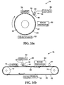
- Fig. 10a is a schematic representation of a drum-based electrophotography machine 74 incorporating a second embodiment of a system for reducing residual potential in a photoconductor, in accordance with the present invention.
- the electrophotography machine 74 substantially corresponds to that shown in Fig. 9a.
- conditioning means 56 is positioned between a surface charge means 76, comprising a scorotron or charging roller, and imaging discharge means 50, relative to the direction of travel of drum 46.
- the scorotron or charging roller of surface charge means 76 still functions as the charge means of the present invention, but does not include a slot for transmission of the conditioning radiation.
- conditioning means 56 transmits conditioning radiation to imaging surface 22 at a point following application of the charge by charge means 76, thereby releasing trapped charge carriers.
- the conditioning radiation is applied after the corona current from the scorotron, the applied surface charge nevertheless maintains the electric field necessary to sweep the released charge carriers out of photoconductor 20.
- the conditioning radiation is tuned to the relevant trap energies, and therefore preferably comprises only wavelengths that fall outside of the absorption band for photoconductor 20, substantially no discharge occurs prior to rotation of drum 46 to the position of imaging discharge means 50. As a result, the uniform surface charge on imaging surface 22 is preserved for the formation of a latent image by the imaging laser.
- Fig. 10b is a schematic representation of a belt-based electrophotography machine 78 incorporating the second embodiment of a system for reducing residual potential in a photoconductor, in accordance with the present invention.
- the electrophotography machine 78 substantially corresponds to that shown in Fig. 10a, but includes a belt 68 mounted on rollers 70, 72.
- the belt 68 carries photoconductor 20 and moves under power of a motor (not shown) coupled to either roller 70 or 72.
- the belt 68 moves in a direction of travel relative to the imaging hardware provided by surface charge means 76, imaging discharge means 50, and development charge means 52.
- conditioning means 56 is positioned proximate to imaging surface 22 between surface charge means 76 and imaging discharge means 50, and therefore follows application of the uniform surface charge to the imaging surface.
- Fig. 11a is a schematic representation of a drum-based electrophotography machine 80 incorporating a third embodiment of a system for reducing residual potential in a photoconductor, not covered by the present invention.
- the electrophotography machine 80 substantially corresponds to that shown in Fig. 9a.
- conditioning means 56 is positioned after development charge means 52 and before surface charge means 76, comprising the scorotron or charging roller, relative to the direction of movement of drum 46. It may be important to also position conditioning means 52 before the toner transfer means (not shown) associated with electrophotography machine 80 for application of conditioning radiation prior to alteration of the electric field by the toner transfer means.
- the charge means is provided not by surface charge means 76, but by development charge means 52, which applies the development bias potential necessary for toner development.
- the conditioning means 56 exposes imaging surface 22 to conditioning radiation at a position following the development of the latent image by development charge means 52.
- the development bias potential maintains a field that is sufficient to sweep the charge carriers released by the conditioning radiation out of photoconductor 20.
- Fig. 11b is a schematic representation of a belt-based electrophotography machine 82 incorporating a system for reducing residual potential in the photoconductor, not covered by the present invention.
- the electrophotography machine 82 substantially corresponds to that shown in Fig. 11a, but includes belt 68 mounted on rollers 70, 72.
- conditioning means 56 is positioned proximate to imaging surface 22 between development charge means 52 and surface charge means 76, relative to a direction of travel of belt 68.
- the conditioning radiation therefore follows application of the development bias potential by development charge means 52, which functions as the charge means.
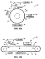
- Fig. 12a is a schematic representation of a drum-based electrophotography machine 84 incorporating a fourth embodiment of a system for reducing residual potential in a photoconductor, not covered by the present invention.
- the electrophotography machine 84 shown in Fig. 12a substantially corresponds to that shown in Fig. 9a, but may correspond to any of the electrophotography machines shown in Figs. 9a, 10a, or 11a.
- the distinction between the electrophotography machine 84 of Fig. 12a is the incorporation of an erase lamp 86. As shown in Fig. 12a, erase lamp 86 may be positioned after development charge means 52 and before surface charge means 48, relative to the direction of movement of drum 46.
- erase lamp 86 exposes imaging surface 22 to broad-spectrum erase radiation that uniformly generates charge carriers and discharges imaging surface 22 immediately prior to application of surface charge means 48.
- the conditioning means 56 exposes imaging surface 22 to conditioning radiation in the presence of the field induced by charge means 48. The field is sufficient to sweep the charge carriers generated by conditioning means 56 out of photoconductor 20.
- Fig. 12b is a schematic representation of a belt-based electrophotography machine 88 incorporating a system for reducing residual potential in the photoconductor, not covered by the present invention.
- the electrophotography machine 88 substantially corresponds to that shown in Fig. 12a, but includes belt 68 mounted on rollers 70, 72.
- erase lamp 86 is positioned proximate to imaging surface 22 between development charge means 52 and charge means 48, relative to a direction of travel of belt 68.
- This example illustrates the effect of the position and type of the conditioning means on the depth of residual potential in an organic photoconductor.
- An organic photoconductor was prepared using the following coating solution: X-form metal-free Phthalocyanine pigment (available from ICI Specialities) 6.4g Butvar® B-76 (polyvinyl butyral available from Monsanto Co.) 32 .0g CAO-5 (2,2'-methylene-bis-6-(t-butyl)-p-cresol, available from Sherwin-Williams) 1.6g Tetrahydrofuran 3 65.0g
- Butvar® B-76 resin was dissolved in tetrahydrofuran followed by the addition of the remaining ingredients and 680g of yellow ceramic beads in a 907 g (32 ounce) glass jar. The mixture was placed on a roller mill at 60 revolutions-per-minute for 48 hours. The solution was decanted off of the ceramic beads and then coated onto an aluminum vapored coated 0.1 mm (4 mil) polyester substrate at a 100 micron wet thickness, using a #40 Meyer rod. The coated substrate was air dried at room temperature for 5 minutes, followed by heating in a convection oven at 90°C for 2 hours.
- the corona charging device used was a scorotron equipped with an illumination slot.
- the infrared (IR) lamp utilized was a linear filament 2700 watt quartz infrared (IR) lamp equipped with a bandpass filter, allowing transmission only between one-thousand (1000) and four-thousand five-hundred (4500) nanometers. Other wavelengths were blocked from the photoconductor by a copper shield positioned around the lamp and filter.
- the IR lamp, filter, and shield arrangement was positioned between the scorotron and the imaging device.
- This example illustrates the effect of IR irradiation on the surface electrostatic potential of a discharged imaged organic photoconductor.
- a photoconductive drum comprising an aluminum drum, organic photoconductive layer, barrier layer and release layer, was prepared as follows: Organic Photoconductive layer coating solution: Millbase: X-form metal-free Phthalocyanine pigment (available from Zeneca Corp.) 100g EC-130 (vinyl chloride copolymer, available from Sekisui; 15% by weight in tetrahydrofuran) 400g Mowital B60HH (polyvinylbutyral resin, available from Hoechst Celanese; 15% by weight in tetrahydrofuran) 600g Tetrahydrofuran 1000g
- the materials listed above were mixed together in a 3.7854 l (1 gallon) glass bottle. The mixture was then milled in a 250 ml horizontal sandmill with 0.8mm ceramic milling media for 24 hours at a rotor speed of 4,000 rpm.
- a coating solution was then prepared by mixing the following materials: Millbase prepared above (12.4% by weight in THF) 300g Tinuvin-770 (UV stabilizer available from Ciba Geigy) 2.2g Mowital B60HH (polyvinylbutyral resin, available from Hoechst Celanese) 296g Tetrahydrofuran (THF) 132g Propyleneglycolmonomethyl ether acetate (PMAc) 79g
- Butvar® B-98 polyvinylbutyral, available from Monsanto
- Triton® X-100 Octylphenoxypolyethoxyethanol, available from Union Carbide Chemicals & Plastics Co. 10% by weight in water
- Deionized water 64.0g
- Ethanol 80.0g 3-Glycidoxypropyltrimethoxysilane (5% prehydrolyzed, available from Huls America) 10.0g
- the above ingredients were combined in the order listed.
- the solution was agitated on a shaker table for 30 minutes, stirred and then allowed to stand for 24 hours.
- the coating solution was coated onto the photoconductor described above using a ring coating process.
- the coating was then cured at 125°C for 30 minutes to give a dry coating thickness of 0.4 micron.
- Vinylmethyl dimethylsiloxane copolymer (trimethylsiloxy terminated having a 27.6 mole % vinylmethyl; 15% by weight in heptane) 3.8g NM203 (polymethylhydrosiloxane, available from Huls America) 0.2g Heptane 20.0g C-158 (vinylmethyl dimethylsiloxane copolymer, trimethylsiloxy terminated having 0.2 mole % vinylmethyl, available from Wacker Silicones) 1.2g Platinum catalyst (1% by weight chloroplatinic acid based hydrosilylation catalyst in heptane) 0.4g
- the above ingredients were combined in the order listed.
- the coating solution was ring coated onto the barrier layer described above.
- the coating was then placed in an 150°C oven for 45 minutes to give a dry coating thickness of 0.7 micron.
- the imaging process consisted of imaging the organic photoconductor using a 780 nanometer laser diode scanner to discharge selected areas of the photoconductor.
- the electrostatic latent image was toned with a magenta liquid toner.
- the toned images were transferred off the photoconductor onto a receptor or other suitable means for image transfer to a receptor.
- the organic photoconductor was then transported beneath the scorotron to recharge the photoconductor to begin the next imaging cycle.
- the imaging cycle was repeated several times with no near infrared/infrared radiation conditioning.
- a new image cycle was then performed to measure optical density and test for ghosts.
- This cycle consisted of uniform exposure by imaging radiation across both the previously imaged and non-imaged areas of the recharged organic photoconductor. After development and transfer to paper, the optical density of the toned image was measured. In the previously imaged areas, the optical densities of the reproduced toned image increased from 0.45 to 0.68 upon treatment of the photoconductor with near infrared/infrared radiation. In the previously non-imaged areas, the optical densities of the reproduced toned image increased from 0.60 to 0.68 upon treatment of the photoconductor with near infrared/infrared radiation. The optical densities were measured using a Gretag SPM50 densitometer set to NCT standards.
- the near infrared and infrared radiation treatment can be accomplished by illuminating the photoconductor with IR radiation either through the scorotron (not covered by the present invention) or between the scorotron and the imaging device. Both methods gave rise to the same average results.
Landscapes
- Physics & Mathematics (AREA)
- General Physics & Mathematics (AREA)
- Discharging, Photosensitive Material Shape In Electrophotography (AREA)
- Exposure Or Original Feeding In Electrophotography (AREA)
- Control Or Security For Electrophotography (AREA)
Claims (14)
- Verfahren zur Verringerung von elektrostatischem Restpotential in einem Photoleiter in einem elektrophotographischen Abbildungsverfahren, wobei das Verfahren die folgenden Schritte aufweist:Aufbringen einer Ladung auf eine Oberfläche des Photoleiters, wobei die Ladung ein elektrisches Feld quer durch den Photoleiter aufbaut, undBelichten des Photoleiters mit Konditionierungsstrahlung mit Wellenlängen, die ausgewählt werden, um Ladungsträger aus Einfangstellen in dem Photoleiter freizusetzen, wobei die Konditionierungsstrahlung im wesentlichen aus Konditionierungsstrahlung mit Wellenlängen besteht, die größer als ein Absorptionsband des Photoleiters sind, wobei die freigesetzten Ladungsträger unter dem Einfluß des elektrischen Felds in dem Photoleiter transportiert werden, um das elektrostatische Restpotential in dem Photoleiter zu verringern,wobei sich der Photoleiter während einem Abbildungszyklus in einer Laufrichtung bewegt und der Belichtungsschritt das Belichten des Photoleiters während dem Abbildungszyklus an einer Position relativ zur Laufrichtung des Photoleiters nach einer Position, an der die genannte Ladung aufgetragen wird, und vor einer Position, an der Bildentladungsstrahlung auf den Photoleiter aufgetragen wird, aufweist.
- Verfahren nach Anspruch 1, wobei der Schritt des Aufbringens der Ladung das Aufbringen der Ladung mit einem unmittelbar bei der Oberfläche des Photoleiters positionierten Scorotron aufweist.
- Verfahren nach Anspruch 1, wobei die Konditionierungsstrahlung im wesentlichen aus Konditionierungsstrahlung mit Wellenlängen besteht, die größer oder gleich 1000 Nanometer sind.
- Verfahren nach Anspruch 3, wobei die Konditionierungsstrahlung im wesentlichen aus Konditionierungsstrahlung mit Wellenlängen in einem Bereich von 1000 bis 4500 Nanometer besteht.
- Verfahren nach Anspruch 1, wobei der Schritt des Belichtens des Photoleiters das Belichten des Photoleiters mit Hilfe einer Konditionierungsstrahlungsquelle aufweist, die unmittelbar bei der Oberfläche des Photoleiters positioniert ist, wobei die Konditionierungsstrahlungsquelle die Konditionierungsstrahlung über ein Filter emittiert.
- Verfahren nach Anspruch 1, wobei der Photoleiter eine Photoleitertrommel ist.
- Verfahren nach Anspruch 1, wobei der Photoleiter ein Photoleiterband ist.
- Verfahren nach Anspruch 1, wobei der Photoleiter ein organisches photoleitendes Material aufweist.
- Verfahren nach Anspruch 1, wobei der Photoleiter ein anorganisches photoleitendes Material aufweist.
- Verfahren nach Anspruch 1, das ferner den Schritt des Wiederholens der Schritte des Aufbringens der Ladung und des Belichtens des Photoleiters ansprechend auf das Verstreichen einer vorbestimmten Nichtbenutzungsdauer des Photoleiters aufweist.
- Verfahren nach Anspruch 1, das ferner den Schritt des Wiederholens der Schritte des Aufbringens der Ladung und des Belichtens des Photoleiters ansprechend auf das Verstreichen einer vorbestimmten Zeitdauer aufweist.
- Verfahren nach Anspruch 1, das ferner die Schritte des Messens eines elektrostatischen Restpotentials des Photoleiters und Wiederholen der Schritte des Aufbringens der Ladung und des Belichtens des Photoleiters, wenn das gemessene elektrostatische Restpotential eine vorbestimmte Schwelle überschreitet, aufweist.
- Vorrichtung zur Implementierung des Verfahrens nach einem der Ansprüche 1 bis 12.
- System zur Verringerung von elektrostatischem Restpotential in einem Photoleiter in einer elektrophotographischen Abbildungsvorrichtung, wobei das System aufweist:eine Aufladungseinrichtung zum Aufbringen einer Ladung auf eine Oberfläche des Photoleiters, wobei die Ladung ein elektrisches Feld quer durch den Photoleiter aufbaut,eine Konditionierungsvorrichtung zum Belichten des Photoleiters mit Konditionierungsstrahlung mit Wellenlängen, die ausgewählt werden, um Ladungsträger aus Einfangstellen in dem Photoleiter freizusetzen, wobei die Konditionierungsstrahlung im wesentlichen aus Konditionierungsstrahlung mit Wellenlängen besteht, die größer als ein Absorptionsband des Photoleiters sind, wobei die freigesetzten Ladungsträger unter dem Einfluß des elektrischen Felds in dem Photoleiter transportiert werden, um das elektrostatische Restpotential in dem Photoleiter zu verringern,eine unmittelbar bei der Oberfläche des Photoleiters positionierte Bildentladungsvorrichtung zum Belichten des Photoleiters mit Entladungsstrahlung, um ein latentes Bild auf dem Photoleiter zu definieren, wobei der Photoleiter sich während einem Abbildungszyklus in einer Laufrichtung bewegt und die Konditionierungsvorrichtung relativ zur Laufrichtung des Photoleiters während dem Abbildungszyklus nach der Aufladungseinrichtung und vor der Bildentladungsvorrichtung positioniert ist.
Priority Applications (1)
| Application Number | Priority Date | Filing Date | Title |
|---|---|---|---|
| EP98122502A EP0917016A1 (de) | 1995-04-28 | 1996-03-08 | Verringerung von restpotential und Geisterbildungsformung in einem Photoleiter |
Applications Claiming Priority (3)
| Application Number | Priority Date | Filing Date | Title |
|---|---|---|---|
| US08/430,432 US5606398A (en) | 1995-04-28 | 1995-04-28 | Reduction of residual potential and ghosting in a photoconductor |
| US430432 | 1995-04-28 | ||
| PCT/US1996/003093 WO1996034321A1 (en) | 1995-04-28 | 1996-03-08 | Reduction of residual potential and ghosting in a photoconductor |
Related Child Applications (1)
| Application Number | Title | Priority Date | Filing Date |
|---|---|---|---|
| EP98122502A Division EP0917016A1 (de) | 1995-04-28 | 1996-03-08 | Verringerung von restpotential und Geisterbildungsformung in einem Photoleiter |
Publications (2)
| Publication Number | Publication Date |
|---|---|
| EP0823075A1 EP0823075A1 (de) | 1998-02-11 |
| EP0823075B1 true EP0823075B1 (de) | 1999-10-13 |
Family
ID=23707544
Family Applications (2)
| Application Number | Title | Priority Date | Filing Date |
|---|---|---|---|
| EP98122502A Withdrawn EP0917016A1 (de) | 1995-04-28 | 1996-03-08 | Verringerung von restpotential und Geisterbildungsformung in einem Photoleiter |
| EP96908692A Expired - Lifetime EP0823075B1 (de) | 1995-04-28 | 1996-03-08 | Verringerung von restpotential und geisterbildformung in einem photoleiter |
Family Applications Before (1)
| Application Number | Title | Priority Date | Filing Date |
|---|---|---|---|
| EP98122502A Withdrawn EP0917016A1 (de) | 1995-04-28 | 1996-03-08 | Verringerung von restpotential und Geisterbildungsformung in einem Photoleiter |
Country Status (6)
| Country | Link |
|---|---|
| US (1) | US5606398A (de) |
| EP (2) | EP0917016A1 (de) |
| JP (1) | JPH11511863A (de) |
| KR (1) | KR19990008113A (de) |
| DE (1) | DE69604659T2 (de) |
| WO (1) | WO1996034321A1 (de) |
Families Citing this family (8)
| Publication number | Priority date | Publication date | Assignee | Title |
|---|---|---|---|---|
| US5956548A (en) * | 1997-09-30 | 1999-09-21 | Brother Kogyo Kabushiki Kaisha | Image forming apparatus |
| JP2003215891A (ja) * | 2002-01-25 | 2003-07-30 | Sharp Corp | 帯電装置 |
| US6959161B2 (en) * | 2003-10-28 | 2005-10-25 | Xerox Corporation | Photoreceptor for highlight color printing machine |
| US7751170B2 (en) * | 2006-06-02 | 2010-07-06 | The Board Of Trustees Of The Leland Stanford Junior University | Charge management of electrically isolated objects via modulated photoelectric charge transfer |
| US9535359B2 (en) * | 2007-04-30 | 2017-01-03 | Hewlett-Packard Indigo B.V. | Method and system for active decrease of ghost appearance |
| US20080280220A1 (en) * | 2007-05-07 | 2008-11-13 | Xerox Corporation. | Electrophotographic imaging member and method of making same |
| US7920810B2 (en) * | 2007-08-15 | 2011-04-05 | Hewlett-Packard Development Company, L.P. | Electrophotography device with electric field applicator |
| US10191407B2 (en) | 2015-04-15 | 2019-01-29 | Hp Indigo B.V. | Applying a corrective voltage |
Family Cites Families (21)
| Publication number | Priority date | Publication date | Assignee | Title |
|---|---|---|---|---|
| JPS4910700B1 (de) * | 1968-11-30 | 1974-03-12 | ||
| DE2635731C2 (de) * | 1976-08-09 | 1982-06-24 | Siemens AG, 1000 Berlin und 8000 München | Vorrichtung für ein Elektrofotografisches Verfahren |
| JPS5381121A (en) * | 1976-12-27 | 1978-07-18 | Kip Kk | Method of taking electrophotography and device therefor |
| JPS53148444A (en) * | 1977-05-27 | 1978-12-25 | Xerox Corp | Electrostatic copying machine |
| DE2726805C3 (de) * | 1977-06-14 | 1981-01-22 | Siemens Ag, 1000 Berlin Und 8000 Muenchen | Elektrofotografische Kopiervorrichtung mit einer Einrichtung zum Loschen eines elektrostatischen Ladungsbildes |
| US4413897A (en) * | 1979-10-31 | 1983-11-08 | Tokyo Shibaura Denki Kabushiki Kaisha | Electrostatic copying apparatus |
| JPS56104371A (en) * | 1980-01-24 | 1981-08-20 | Toshiba Corp | Method for prevention of fatigue of photoreceptor in electrophotographic copier |
| JPS59155879A (ja) * | 1983-02-25 | 1984-09-05 | Fuji Xerox Co Ltd | 静電荷除去装置 |
| US4641158A (en) * | 1984-02-13 | 1987-02-03 | Canon Kabushiki Kaisha | Electrophotographic apparatus |
| JPS6197667A (ja) * | 1984-10-17 | 1986-05-16 | Sharp Corp | 電子写真感光体の帯電電位安定化方法 |
| DE3536836A1 (de) * | 1984-10-17 | 1986-04-17 | Sharp K.K., Osaka | Entladevorrichtung fuer ein kopiergeraet |
| JPS6199184A (ja) * | 1984-10-22 | 1986-05-17 | Sharp Corp | 電子写真感光体の除電方法 |
| JPS61145576A (ja) * | 1984-12-19 | 1986-07-03 | Sharp Corp | 感光体の表面電位補正方法 |
| JPS61185778A (ja) * | 1985-02-13 | 1986-08-19 | Sanyo Electric Co Ltd | 静電記録装置 |
| DE3769100D1 (de) * | 1986-12-09 | 1991-05-08 | Konishiroku Photo Ind | Verfahren zur herstellung eines bildes. |
| JPH01297695A (ja) * | 1988-05-25 | 1989-11-30 | Canon Inc | 電子写真装置 |
| JPH0293484A (ja) * | 1988-09-29 | 1990-04-04 | Mita Ind Co Ltd | 感光ドラムの除電装置 |
| US5055879A (en) * | 1989-06-02 | 1991-10-08 | Compaq Computer Corporation | Apparatus for ozoneless efficient charging of a photoreceptive drum in an electrophotographic printer |
| US5083163A (en) * | 1990-07-16 | 1992-01-21 | Minnesota Mining & Manufacturing Company | Photoconductor resetting following multiple charge images |
| US5272504A (en) * | 1990-11-07 | 1993-12-21 | Minolta Camera Kabushiki Kaisha | Device for erasing residual charge on photosensitive member |
| US5510626A (en) * | 1994-06-22 | 1996-04-23 | Minnesota Mining And Manufacturing Company | System and method for conditioning a radiation detector |
-
1995
- 1995-04-28 US US08/430,432 patent/US5606398A/en not_active Expired - Fee Related
-
1996
- 1996-03-08 KR KR1019970707638A patent/KR19990008113A/ko not_active Ceased
- 1996-03-08 EP EP98122502A patent/EP0917016A1/de not_active Withdrawn
- 1996-03-08 JP JP8532494A patent/JPH11511863A/ja active Pending
- 1996-03-08 DE DE69604659T patent/DE69604659T2/de not_active Expired - Fee Related
- 1996-03-08 WO PCT/US1996/003093 patent/WO1996034321A1/en not_active Ceased
- 1996-03-08 EP EP96908692A patent/EP0823075B1/de not_active Expired - Lifetime
Also Published As
| Publication number | Publication date |
|---|---|
| DE69604659D1 (de) | 1999-11-18 |
| WO1996034321A1 (en) | 1996-10-31 |
| US5606398A (en) | 1997-02-25 |
| KR19990008113A (ko) | 1999-01-25 |
| EP0917016A1 (de) | 1999-05-19 |
| DE69604659T2 (de) | 2000-11-30 |
| EP0823075A1 (de) | 1998-02-11 |
| JPH11511863A (ja) | 1999-10-12 |
Similar Documents
| Publication | Publication Date | Title |
|---|---|---|
| US4538901A (en) | Electrophotographic copier with a phantom image suppression function | |
| EP0823075B1 (de) | Verringerung von restpotential und geisterbildformung in einem photoleiter | |
| US4785324A (en) | Electrophotographic apparatus and method for preventing the lowering of a charging voltage at a photoreceptor | |
| US4607934A (en) | Electrophotography using a photosensitive drum with multi-photosensitive layers sensitive to different wave lengths | |
| US5038177A (en) | Selective pre-transfer corona transfer with light treatment for tri-level xerography | |
| JP3379803B2 (ja) | 2波長単一光学系ros及び2層形感光体を用いたカラーゼログラフィ印刷装置 | |
| EP0467609B1 (de) | Verfahren und Gerät zum mehrfachen elektrischen Laden einer Photoleiterschicht | |
| US4529292A (en) | Electrophotographic reproduction process | |
| US4119373A (en) | Electrographic apparatus and method for using arsenic selenide as the photoconductor | |
| US4392737A (en) | Electrophotographic copying apparatus | |
| US4433038A (en) | Electrophotographic copying process involving simultaneous charging and imaging | |
| US4645330A (en) | Electrophotographic device | |
| US4442191A (en) | Electrophotographic copying process for producing a plurality of copies | |
| US4440844A (en) | Electrophotographic copying process involving simultaneous charging and imaging | |
| US6223011B1 (en) | Printing machine with reconditioning light source | |
| US6208819B1 (en) | Method for discharging photoreceptor residual charges | |
| US20030123901A1 (en) | Printing machine discharge device including pluralities of emitters for different degrees of image receiver charge manipulation | |
| JPH0464069B2 (de) | ||
| US4362797A (en) | Electrophotographc process to release trapped charges by charging and ultraviolet exposure | |
| JPS6064364A (ja) | 画像形成方法および装置 | |
| JPH01191174A (ja) | 画像形成装置 | |
| JP3432093B2 (ja) | 画像形成装置 | |
| JPH05165387A (ja) | ランプ光量設定方法 | |
| JPH04220683A (ja) | 感光体除電装置 | |
| JPH01191175A (ja) | 画像形成装置 |
Legal Events
| Date | Code | Title | Description |
|---|---|---|---|
| PUAI | Public reference made under article 153(3) epc to a published international application that has entered the european phase |
Free format text: ORIGINAL CODE: 0009012 |
|
| 17P | Request for examination filed |
Effective date: 19971126 |
|
| AK | Designated contracting states |
Kind code of ref document: A1 Designated state(s): DE FR GB IT |
|
| 17Q | First examination report despatched |
Effective date: 19980313 |
|
| GRAG | Despatch of communication of intention to grant |
Free format text: ORIGINAL CODE: EPIDOS AGRA |
|
| GRAG | Despatch of communication of intention to grant |
Free format text: ORIGINAL CODE: EPIDOS AGRA |
|
| GRAG | Despatch of communication of intention to grant |
Free format text: ORIGINAL CODE: EPIDOS AGRA |
|
| GRAH | Despatch of communication of intention to grant a patent |
Free format text: ORIGINAL CODE: EPIDOS IGRA |
|
| GRAH | Despatch of communication of intention to grant a patent |
Free format text: ORIGINAL CODE: EPIDOS IGRA |
|
| GRAA | (expected) grant |
Free format text: ORIGINAL CODE: 0009210 |
|
| AK | Designated contracting states |
Kind code of ref document: B1 Designated state(s): DE FR GB IT |
|
| PG25 | Lapsed in a contracting state [announced via postgrant information from national office to epo] |
Ref country code: IT Free format text: LAPSE BECAUSE OF FAILURE TO SUBMIT A TRANSLATION OF THE DESCRIPTION OR TO PAY THE FEE WITHIN THE PRESCRIBED TIME-LIMIT;WARNING: LAPSES OF ITALIAN PATENTS WITH EFFECTIVE DATE BEFORE 2007 MAY HAVE OCCURRED AT ANY TIME BEFORE 2007. THE CORRECT EFFECTIVE DATE MAY BE DIFFERENT FROM THE ONE RECORDED. Effective date: 19991013 Ref country code: FR Free format text: LAPSE BECAUSE OF FAILURE TO SUBMIT A TRANSLATION OF THE DESCRIPTION OR TO PAY THE FEE WITHIN THE PRESCRIBED TIME-LIMIT Effective date: 19991013 |
|
| REF | Corresponds to: |
Ref document number: 69604659 Country of ref document: DE Date of ref document: 19991118 |
|
| PGFP | Annual fee paid to national office [announced via postgrant information from national office to epo] |
Ref country code: DE Payment date: 19991229 Year of fee payment: 5 |
|
| PG25 | Lapsed in a contracting state [announced via postgrant information from national office to epo] |
Ref country code: GB Free format text: LAPSE BECAUSE OF NON-PAYMENT OF DUE FEES Effective date: 20000308 |
|
| EN | Fr: translation not filed | ||
| PG25 | Lapsed in a contracting state [announced via postgrant information from national office to epo] |
Ref country code: DE Free format text: LAPSE BECAUSE OF FAILURE TO SUBMIT A TRANSLATION OF THE DESCRIPTION OR TO PAY THE FEE WITHIN THE PRESCRIBED TIME-LIMIT Effective date: 20000324 |
|
| PLBE | No opposition filed within time limit |
Free format text: ORIGINAL CODE: 0009261 |
|
| STAA | Information on the status of an ep patent application or granted ep patent |
Free format text: STATUS: NO OPPOSITION FILED WITHIN TIME LIMIT |
|
| 26N | No opposition filed | ||
| GBPC | Gb: european patent ceased through non-payment of renewal fee |
Effective date: 20000308 |