EP0820060A1 - Verfahren und Gerät zur Optimierung der Leistung in Signalkanälen - Google Patents
Verfahren und Gerät zur Optimierung der Leistung in Signalkanälen Download PDFInfo
- Publication number
- EP0820060A1 EP0820060A1 EP97103244A EP97103244A EP0820060A1 EP 0820060 A1 EP0820060 A1 EP 0820060A1 EP 97103244 A EP97103244 A EP 97103244A EP 97103244 A EP97103244 A EP 97103244A EP 0820060 A1 EP0820060 A1 EP 0820060A1
- Authority
- EP
- European Patent Office
- Prior art keywords
- signal
- noise
- channel
- coupled
- combined
- Prior art date
- Legal status (The legal status is an assumption and is not a legal conclusion. Google has not performed a legal analysis and makes no representation as to the accuracy of the status listed.)
- Withdrawn
Links
- 238000000034 method Methods 0.000 title claims abstract description 23
- 238000012360 testing method Methods 0.000 claims description 18
- 238000001514 detection method Methods 0.000 claims description 6
- 230000008878 coupling Effects 0.000 claims description 4
- 238000010168 coupling process Methods 0.000 claims description 4
- 238000005859 coupling reaction Methods 0.000 claims description 4
- 230000003595 spectral effect Effects 0.000 claims description 4
- 238000001914 filtration Methods 0.000 claims 1
- 239000000872 buffer Substances 0.000 abstract description 12
- 238000003860 storage Methods 0.000 description 15
- 238000010586 diagram Methods 0.000 description 6
- 238000004519 manufacturing process Methods 0.000 description 6
- 238000005457 optimization Methods 0.000 description 6
- 230000008569 process Effects 0.000 description 6
- 238000012545 processing Methods 0.000 description 4
- 230000006870 function Effects 0.000 description 3
- 238000005259 measurement Methods 0.000 description 3
- 238000007476 Maximum Likelihood Methods 0.000 description 2
- 238000013459 approach Methods 0.000 description 2
- 239000003990 capacitor Substances 0.000 description 2
- 238000013500 data storage Methods 0.000 description 2
- 230000005669 field effect Effects 0.000 description 2
- 230000015654 memory Effects 0.000 description 2
- 230000004044 response Effects 0.000 description 2
- 238000013019 agitation Methods 0.000 description 1
- 238000012512 characterization method Methods 0.000 description 1
- 238000011161 development Methods 0.000 description 1
- 230000018109 developmental process Effects 0.000 description 1
- 230000000694 effects Effects 0.000 description 1
- 238000011156 evaluation Methods 0.000 description 1
- 239000000463 material Substances 0.000 description 1
- 230000007246 mechanism Effects 0.000 description 1
- 238000011084 recovery Methods 0.000 description 1
- 239000004065 semiconductor Substances 0.000 description 1
- 230000020347 spindle assembly Effects 0.000 description 1
Images
Classifications
-
- H—ELECTRICITY
- H03—ELECTRONIC CIRCUITRY
- H03F—AMPLIFIERS
- H03F3/00—Amplifiers with only discharge tubes or only semiconductor devices as amplifying elements
- H03F3/45—Differential amplifiers
-
- G—PHYSICS
- G11—INFORMATION STORAGE
- G11B—INFORMATION STORAGE BASED ON RELATIVE MOVEMENT BETWEEN RECORD CARRIER AND TRANSDUCER
- G11B20/00—Signal processing not specific to the method of recording or reproducing; Circuits therefor
- G11B20/10—Digital recording or reproducing
- G11B20/18—Error detection or correction; Testing, e.g. of drop-outs
- G11B20/1816—Testing
- G11B20/182—Testing using test patterns
-
- G—PHYSICS
- G11—INFORMATION STORAGE
- G11B—INFORMATION STORAGE BASED ON RELATIVE MOVEMENT BETWEEN RECORD CARRIER AND TRANSDUCER
- G11B5/00—Recording by magnetisation or demagnetisation of a record carrier; Reproducing by magnetic means; Record carriers therefor
- G11B5/012—Recording on, or reproducing or erasing from, magnetic disks
Definitions
- This invention relates to the field of optimizing the performance of signal channels, and, more specifically, to optimizing the performance of integrated circuit disk drive read channels.
- the data synchronizer performs sync field search and data synchronization.
- the data synchronizer uses a phase locked loop (PLL) to provide data synchronization and to develop a decode window.
- the window shift circuit shifts the phase of the voltage controlled oscillator (VCO) of the PLL to effectively shift the relative position of the read data pulse within the decode window.
- the write precompensation circuit uses the data synchronizer to provide data encoding and independent late/early write precompensation for NRZ data.
- the ENDEC provides encoding and decoding, preferably of run length limited (RLL) signals.
- the control circuit co-ordinates and controls the operation of the aforementioned circuits and subsystems.
- the present invention is applicable generally to devices in which signal channel variations caused by the manufacturing process significantly affect the signal quality.
- Examples of devices that may be improved by using the present invention include: modems, tape drives, magneto-optical drives, and disk drives.
- resistors are used as a noise generator.
- a buffer and pre-amplifier stage isolate the noise generator and amplifies the noise signal.
- the amplitude of the noise signal is controlled by a programmable multiplier.
- the multiplier is programmed through a differential current digital-to-analogue converter.
- a filter circuit limits the noise bandwidth.
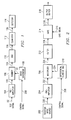
- the test signal 102 may originate from a magnetic storage media, for example a magnetic disk read back head.
- Pre-amplifier 104 amplifies the test signal 102 and provides a pre-amplifier output through node 120 to summer 106.
- the test signal is combined with the output of the noise generator 108 in summer 106.
- noise generator 108 is in a signal channel integrated circuit.
- noise generator 108 could be in a separate integrated circuit, but where noise generator 108 and the signal channel are still inside a single device, for example a disk drive.
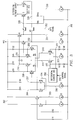
- Transistors Q1, Q2, Q3, Q4, resistors R3, R4, and current sources I1, I2 and I3 form a buffer and pre-amplifier stage.
- Resistor R1 is coupled to the base of transistor Q1.
- the collector of transistor Q1 is coupled to VCC through node 302.
- the emitter of transistor Q1 is coupled to current source I3 through node 305.
- Resistor R2 is coupled to the base of transistor Q2.
- the collector transistor Q2 is coupled to VCC through node 302.
- the emitter of transistor Q2 is coupled to current source I1 through node 324.
- Current sources I1 and I3 are coupled to ground through node 300.
- I3 is proportional to absolute temperature (PTAT) current source.
- the differential current DAC is provided from the differential current DAC.
- One Gilbert Cell Multiplier input is formed by nodes 307 and 304, and the other input is formed by nodes 320 and 321.
- the Gilbert Cell Multiplier output is formed by nodes 310 and 316.
- Diodes D3, D4, D5, and D6 with transistors Q11 and Q12 form the control section of the Gilbert Multiplier Cell.
- Transistors Q11 and Q12 form an emitter-coupled pair.
- the collector of transistor Q11 is coupled to the emitters of transistors Q7 and Q8 through node 314.
- the collector of transistor Q12 is coupled to resistors R5 and R6 through node 318.
- the base of transistor Q11 is coupled to differential current DAC 350, and to diode D3 through node 320.
- Diode D3 is coupled to diode D4.
- Diode D4 is coupled to node 300.
- the base of transistor Q12 is coupled to differential current DAC 350 and diode D5 through node 321.
- Diode D5 is coupled to diode D6.
- Diode D6 is coupled to ground through node 300.
- the emitters of transistors Q11 and Q12 are coupled to current source I4 through node 322.
- Current source I4 is coupled to ground through node 300.
- the emitter of transistor Q9 is coupled to current source I5 through node 332.
- the emitter of transistor Q10 is coupled to current source I6 through node 334.
- Current sources I5 and I6 are coupled to ground through node 300.
- FETs M1 and M2 form a gate to open and close the coupling between the Gilbert Cell Multiplier and the output buffer stage.
- the drain of FET M1 is coupled to the emitter of transistor Q10 through node 334.
- the drain of FET M2 is coupled to the emitter of transistor Q9.
- the gate of FETs M1 and M2 are coupled to gate signal 352, which is used to turn the gates "ON” and "OFF”.
- Resistors R11 and R12 are coupled to current source I7 through node 330.
- Current source 17 is coupled to ground through node 300.
- the collectors of transistor Q13 and Q14 form a differential current output. In the embodiment shown in Figure 2, the differential current output is coupled to summer 106 through node 122.
Landscapes
- Engineering & Computer Science (AREA)
- Signal Processing (AREA)
- Power Engineering (AREA)
- Digital Magnetic Recording (AREA)
- Signal Processing For Digital Recording And Reproducing (AREA)
- Analogue/Digital Conversion (AREA)
- Recording Or Reproducing By Magnetic Means (AREA)
Applications Claiming Priority (2)
| Application Number | Priority Date | Filing Date | Title |
|---|---|---|---|
| US608296 | 1996-02-28 | ||
| US08/608,296 US5914827A (en) | 1996-02-28 | 1996-02-28 | Method and apparatus for implementing a noise generator in an integrated circuit disk drive read channel |
Publications (1)
| Publication Number | Publication Date |
|---|---|
| EP0820060A1 true EP0820060A1 (de) | 1998-01-21 |
Family
ID=24435871
Family Applications (1)
| Application Number | Title | Priority Date | Filing Date |
|---|---|---|---|
| EP97103244A Withdrawn EP0820060A1 (de) | 1996-02-28 | 1997-02-27 | Verfahren und Gerät zur Optimierung der Leistung in Signalkanälen |
Country Status (6)
| Country | Link |
|---|---|
| US (1) | US5914827A (de) |
| EP (1) | EP0820060A1 (de) |
| JP (1) | JPH103756A (de) |
| KR (1) | KR100432834B1 (de) |
| SG (1) | SG45534A1 (de) |
| TW (1) | TW362211B (de) |
Cited By (1)
| Publication number | Priority date | Publication date | Assignee | Title |
|---|---|---|---|---|
| WO2020227488A1 (en) | 2019-05-08 | 2020-11-12 | Bae Systems Information And Electronic Systems Integration Inc. | Apparatus and method for digitally characterizing communication channel noise and interference |
Families Citing this family (5)
| Publication number | Priority date | Publication date | Assignee | Title |
|---|---|---|---|---|
| KR100224731B1 (ko) * | 1997-06-23 | 1999-10-15 | 윤종용 | 논리 디바이스 테스트 장치 및 방법 |
| US6337648B1 (en) * | 1998-11-25 | 2002-01-08 | Texas Instruments Inc. | MOS transistor digital-to-analog converter |
| WO2010053744A1 (en) * | 2008-10-29 | 2010-05-14 | Maxim Integrated Products, Inc. | Rms metering devices and methods |
| US8891192B1 (en) | 2012-11-15 | 2014-11-18 | Western Digital Technologies, Inc. | Disk drive calibrating parameter by injecting noise signal and measuring off-track read capability |
| US9425799B2 (en) * | 2014-03-05 | 2016-08-23 | University Of Hawaii | Reconfigurable logic gates using chaotic dynamics |
Citations (5)
| Publication number | Priority date | Publication date | Assignee | Title |
|---|---|---|---|---|
| DE2947119B1 (de) * | 1979-11-22 | 1981-01-22 | Siemens Ag | Einrichtung zum Feststellen eines einen zulaessigen Hoechstpegel ueberschreitenden Stoersignals einer vorgegebenen Frequenz |
| US4591940A (en) * | 1982-07-13 | 1986-05-27 | Westinghouse Electric Corp. | Signal quality monitor for protective relay system |
| JPS62212577A (ja) * | 1986-03-14 | 1987-09-18 | Fujitsu Ltd | シリンダアクセスのチエツク方式 |
| US4750156A (en) * | 1986-03-03 | 1988-06-07 | Input/Output, Inc. | Noise suppression during seismic exploration |
| WO1996025739A1 (en) * | 1995-02-17 | 1996-08-22 | Conner Peripherals, Inc. | System and method for calibration of a read/write channel |
Family Cites Families (5)
| Publication number | Priority date | Publication date | Assignee | Title |
|---|---|---|---|---|
| US5121263A (en) * | 1989-10-31 | 1992-06-09 | International Business Machines Corporation | Method and apparatus for determining the error rate of magnetic recording disk drives having a amplitude sampling data detection |
| JP2795545B2 (ja) * | 1991-02-01 | 1998-09-10 | シャープ株式会社 | 雑音発生装置 |
| US5172072A (en) * | 1991-09-06 | 1992-12-15 | Itt Corporation | High efficiency harmonic injection power amplifier |
| US5657422A (en) * | 1994-01-28 | 1997-08-12 | Lucent Technologies Inc. | Voice activity detection driven noise remediator |
| KR0153019B1 (ko) * | 1994-09-28 | 1998-11-16 | 정장호 | 가변 대역폭에 대응하여 의사잡음 코드를 생성하는 확산 대역방식의 무선 랜시스템 및 그의 데이타 통신 방법 |
-
1996
- 1996-02-28 US US08/608,296 patent/US5914827A/en not_active Expired - Lifetime
-
1997
- 1997-02-27 SG SG1997000512A patent/SG45534A1/en unknown
- 1997-02-27 KR KR1019970006321A patent/KR100432834B1/ko not_active Expired - Lifetime
- 1997-02-27 EP EP97103244A patent/EP0820060A1/de not_active Withdrawn
- 1997-02-28 JP JP9046381A patent/JPH103756A/ja active Pending
- 1997-03-14 TW TW086103152A patent/TW362211B/zh not_active IP Right Cessation
Patent Citations (5)
| Publication number | Priority date | Publication date | Assignee | Title |
|---|---|---|---|---|
| DE2947119B1 (de) * | 1979-11-22 | 1981-01-22 | Siemens Ag | Einrichtung zum Feststellen eines einen zulaessigen Hoechstpegel ueberschreitenden Stoersignals einer vorgegebenen Frequenz |
| US4591940A (en) * | 1982-07-13 | 1986-05-27 | Westinghouse Electric Corp. | Signal quality monitor for protective relay system |
| US4750156A (en) * | 1986-03-03 | 1988-06-07 | Input/Output, Inc. | Noise suppression during seismic exploration |
| JPS62212577A (ja) * | 1986-03-14 | 1987-09-18 | Fujitsu Ltd | シリンダアクセスのチエツク方式 |
| WO1996025739A1 (en) * | 1995-02-17 | 1996-08-22 | Conner Peripherals, Inc. | System and method for calibration of a read/write channel |
Non-Patent Citations (3)
| Title |
|---|
| DATABASE INSPEC INSTITUTE OF ELECTRICAL ENGINEERS, STEVENAGE, GB; NABEREIT H: "A noise generator for system tests", XP002036534 * |
| H. NABEREIT: "Rauschgenerator zum Systemtest", ELEKTRONIK, 10 FEB. 1984, WEST GERMANY, vol. 33, no. 3, ISSN 0013-5658, pages 65 - 66 * |
| PATENT ABSTRACTS OF JAPAN vol. 012, no. 074 (P - 674) 9 March 1988 (1988-03-09) * |
Cited By (2)
| Publication number | Priority date | Publication date | Assignee | Title |
|---|---|---|---|---|
| WO2020227488A1 (en) | 2019-05-08 | 2020-11-12 | Bae Systems Information And Electronic Systems Integration Inc. | Apparatus and method for digitally characterizing communication channel noise and interference |
| EP3966980A4 (de) * | 2019-05-08 | 2023-04-19 | BAE SYSTEMS Information and Electronic Systems Integration, Inc. | Vorrichtung und verfahren zur digitalen charakterisierung von kommunikationskanalrauschen und -interferenzen |
Also Published As
| Publication number | Publication date |
|---|---|
| KR970063908A (ko) | 1997-09-12 |
| US5914827A (en) | 1999-06-22 |
| KR100432834B1 (ko) | 2004-09-07 |
| TW362211B (en) | 1999-06-21 |
| JPH103756A (ja) | 1998-01-06 |
| SG45534A1 (en) | 1998-01-16 |
Similar Documents
| Publication | Publication Date | Title |
|---|---|---|
| US8359527B1 (en) | Averaging signals to improve signal interpretation | |
| US9881637B1 (en) | Methods and devices for spin torque oscillator control and monitoring | |
| JP2868707B2 (ja) | ディスク状記録担体を利用したデータ記録装置の読出チャンネル最適化方法 | |
| EP0455749B1 (de) | Lese-kanal-detektor zur anwendung in digitalen magnetaufzeichnungssystemen | |
| US5355261A (en) | Method and apparatus for measuring error rate of magnetic recording devices having a partial response maximum likelihood data detection channel | |
| JP3467041B2 (ja) | Mrヘッド読み取り信号前処理回路 | |
| US6014768A (en) | Moving reference channel quality monitor for read channels | |
| US4346411A (en) | Amplitude sensitive three-level detector for derivative read back channel of magnetic storage device | |
| US6031672A (en) | Method and apparatus for servo data pattern detection | |
| JPH0443349B2 (de) | ||
| US6519103B2 (en) | View DAC feedback inside analog front circuit | |
| JPH0159667B2 (de) | ||
| US6731443B2 (en) | Total error multiplier for optimizing read/write channel | |
| US5914827A (en) | Method and apparatus for implementing a noise generator in an integrated circuit disk drive read channel | |
| US6661590B2 (en) | Efficient analog front end for a read/write channel of a hard disk drive running from a highly regulated power supply | |
| Alini et al. | A 200-MSample/s trellis-coded PRML read/write channel with analog adaptive equalizer and digital servo | |
| US6252734B1 (en) | Arrangement for reproducing a digital signal from a track on a magnetic record carrier having an equalizer filter in the form of a transconductance-capacitor filter | |
| KR19980019000A (ko) | 판독 채널 IC의 채널 품질 모니터 및 그 방법(A Channel Quality Monitor for Read Channel IC) | |
| Tan et al. | Signal processing for perpendicular recording channels with intertrack interference | |
| US20050213238A1 (en) | Apparatus for providing head amplitude characterization | |
| US6091562A (en) | Digital magnetic reproducing apparatus and digital magnetic recording/reproducing apparatus employing detection of second harmonic distortion and signal to noise ratio | |
| EP1563500B1 (de) | Ein effizienter analoger front-end für einen lese-/schreibkanal eines festplattenlaufwerks, betrieben mit einer hochregulierten stromversorgung | |
| JPS58199410A (ja) | デイジタル信号の磁気記録方法 | |
| JP2756221B2 (ja) | 復調回路 | |
| Thornley | Compensation of peak-shift with write timing |
Legal Events
| Date | Code | Title | Description |
|---|---|---|---|
| PUAI | Public reference made under article 153(3) epc to a published international application that has entered the european phase |
Free format text: ORIGINAL CODE: 0009012 |
|
| AK | Designated contracting states |
Kind code of ref document: A1 Designated state(s): DE FR GB IT NL |
|
| STAA | Information on the status of an ep patent application or granted ep patent |
Free format text: STATUS: THE APPLICATION IS DEEMED TO BE WITHDRAWN |
|
| 18D | Application deemed to be withdrawn |
Effective date: 19980722 |