EP0820030B1 - Halbleiterfunktionsschaltung - Google Patents
Halbleiterfunktionsschaltung Download PDFInfo
- Publication number
- EP0820030B1 EP0820030B1 EP96907743A EP96907743A EP0820030B1 EP 0820030 B1 EP0820030 B1 EP 0820030B1 EP 96907743 A EP96907743 A EP 96907743A EP 96907743 A EP96907743 A EP 96907743A EP 0820030 B1 EP0820030 B1 EP 0820030B1
- Authority
- EP
- European Patent Office
- Prior art keywords
- circuit
- operational
- signal
- semiconductor
- data
- Prior art date
- Legal status (The legal status is an assumption and is not a legal conclusion. Google has not performed a legal analysis and makes no representation as to the accuracy of the status listed.)
- Expired - Lifetime
Links
Images


Classifications
-
- G—PHYSICS
- G06—COMPUTING; CALCULATING OR COUNTING
- G06G—ANALOGUE COMPUTERS
- G06G7/00—Devices in which the computing operation is performed by varying electric or magnetic quantities
- G06G7/12—Arrangements for performing computing operations, e.g. operational amplifiers
- G06G7/26—Arbitrary function generators
Definitions
- the present invention relates to a semiconductor operational circuit, and in particular, relates to an operational circuit which is applied to high speed image processing or the like.
- image processing For example, if one screen is incorporated into a 500 x 500 two dimensional array, then the total number of pixels is 250, 000, and when the strength of the three colors red, green, and blue for each pixel is expressed in terms of 8 bits, then the amount of data in one stationary image reaches 750,000 bits. In moving images, the amount of image data increases with time.
- An example of this is the detection of movement vectors, which is one the important operations in the processing of moving images. That is to say, in this operation, with respect to the images in two frames which are continuous in time, the amount of motion in the image of the object photographed is determined.
- the image may be moved by ⁇ 8 pixels vertically or horizontally, and the amount of dislocation may be determined by overlaying the images until they line up.
- the amount of dislocation in the image between the two frames is calculated with respect to a total of 64 combinations, and the combination having the smallest amount of dislocation is found. Total calculations of a few tens of GOPS are required, and even if extremely high speed processors are employed on a number of chips in parallel, a period of approximately 30 msec is required. In order to control robots in real time, it is important to conduct the image data processing in 1 msec or less; however, this is completely impossible with current technology.
- the present invention was designed in light of the above circumstances; it has as an object thereof to provide a semiconductor operational circuit which is capable of instantaneously processing in parallel a large quantity of information.
- the semiconductor operational circuit of the present invention which executes a predetermined operation with respect to a first signal train of signals A 1 , A 2 , ..., A N-1 , A N (where N is a positive integer) of N signals numbered from 1 to N, and a second signal train of signals B 1 , B 2 , ..., B M-1 , B M (where M is a positive integer) of M signals numbered from 1 to M, comprising a plurality of first operational circuits for executing a predetermined operation with respect to A i and B i+n (where i is a positive integer and n is a positive or negative integer and 1 ⁇ i ⁇ n and 1 ⁇ i + n ⁇ M) and generating an output signal C i,n , at least one second operational circuit for generating the sum S n of a part or the whole of output signals of the first operational circuits with respect to a predetermined value of n, where i has differing values, or for generating a predetermined signal T
- Figure 1(a) and Figure 1(b) are schematic diagrams explaining a first embodiment of the present invention.
- Figure 2(a) and Figure 2(b) are schematic diagrams explaining the function of the ⁇ X detection circuitry of Figure 1.
- Figure 3 is a schematic diagram showing the circuitry which calculates the sum of C i,n .
- Figure 4 is a schematic diagram showing an amount of motion detector.
- FIG. 5 is a circuit diagram showing an example of a winner-take-all (WTA) circuit.
- Figure 6 (a) shows an example of an absolute value operational circuit
- Figure 6(b) shows the relationship between the input and output thereof.
- Figure 7(a), Figure 7(b), Figure 7(c), and Figure 7(d) illustrate the operation of the absolute value operational circuit.
- Figure 8 is a schematic diagram illustrating a second embodiment of the present invention.
- Figure 9(a) shows another example of an absolute value operational circuit
- Figure 9(b) shows the relationship between the input and output thereof.
- Figure 10 is a graph showing the results of the operation of the absolute value operational circuit of Figure 9.
- FIG 11 is a circuit diagram showing another example of a winner-take-all (WTA) circuit.
- Figure 12 is a graph showing the results of the operation of the circuitry of Figure 8.
- Figure 13 is a graph showing the time t signal and the time t + ⁇ t signal.
- Figure 14 is a schematic diagram illustrating a third embodiment of the present invention.
- Figure 15(a), Figure 15(b), Figure 15(c), Figure 15(d), Figure 15(e), and Figure 15(f) are schematic diagrams illustrating the detection principle of the third embodiment.
- Figure 16 is a schematic diagram illustrating a fourth embodiment of the present invention.
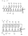
- Figure 17 is a schematic diagram showing an example of a method for setting the gain of each source follower to the same value.
- Figure 18 is a schematic diagram illustrating a method for detaching unnecessary cells.
- Figure 19(a) and Figure 19(b) illustrate the operation of the circuitry when SEARCH (N,M) is executed.
- Figure 20 is a schematic diagram illustrating a fifth embodiment of the present invention.
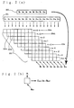
- Figure 1(a) shows a first embodiment of the present invention as a block diagram; this is an operational circuit which detects motion vectors of images captured by an image sensor array 101.
- References 102 and 103 indicate images of an airplane captured at times t and t + ⁇ t, respectively.
- Reference 102' indicates data in which data of each pixel in image 102 (indicating the brightness of each pixel) is totaled with respect to vertical columns and this is plotted along the x axis; these data thus represent a so-called projection of image 102 onto the x axis.
- Reference 103' indicates the x axis projection data of image 103
- 102" and 103" indicate y axis projection data relating to images 102 and 103.
- the circuit of Figure 1(a) determines the amount of movement ⁇ x in the x direction of the aircraft by detecting the displacement in the x axis projection data, and determines the amount of movement ⁇ y in the y direction from the amount of displacement in the y axis projection data, and by means of this detects a movement vector ( ⁇ x, ⁇ y).
- reference 101 indicates a sensor array; here, in order to keep the explanation simple, an 16 x 16 sensor array (a total of 256 cells) was used as an example, but it is of course the case that any number of cells may be employed.
- ⁇ x detection circuit 104 indicates a analog memory which stores 16 data projected on the x axis, for each column of the sensor array, and two groups of values are maintained; the values for time t, and the values for time t + ⁇ t.
- Reference 106 indicates a circuit which obtains the correlation between the two groups of data series.
- the two groups of data series described above are shifted one pixel at a time in the horizontal direction, and the amount of displacement is calculated; in this embodiment, the amount of displacement when a shift of a maximum of 4 pixels is carried out is determined by means of simultaneous parallel operations.
- This output is inputted into amount of movement amount detector 107, and the amount of shift which results in the minimum evaluated amount of displacement is determined, and by means of this, the circuit specifies the amount of movement ⁇ x.
- ⁇ y detection circuit 108 is similar to the ⁇ x detection circuit, and this circuit specifies the amount of movement ⁇ y.
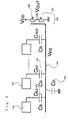
- the X axis projection data trains obtained at time t is A 1 , A 2 , ..., A 16 , and memory 201 stores this temporarily.
- a 1 is stored as a voltage value proportional to the sum of all the sensor outputs of the first column of image sensor array 101.
- B 5 , B 6 , ..., B 12 represents a x axis projection data trains obtained at time t + ⁇ t; the fifth to the twelfth data is stored in memory 202.
- the same data are supplied from memory 201 in the direction shown by the arrows in the figure. That is to say, the data A 1 , A 2 , ..., A 8 are supplied to row 204a, the data A 2 , A 3 ,..., A 9 are supplied to row 204b, and the data A 5 , A 6 ,..., A 12 are supplied to row 204c.
- the same data are supplied from memory 202 in the direction shown in the figure by the arrows.
- the eight data B 5 , B 6 , B 7 ,..., B 12 are supplied to each row, in other words.
- the data A 2 - A 9 from memory 201, and the data B 5 - B 12 from memory 202, are supplied to the cells of row 204b, so that
- n 3 and the B data are shifted to the left by 3 pixels with respect to the A data, and the absolute value of the difference therebetween is obtained.
- each cell 301, 302, and the like are circuits identical to those in Figure 2(b); the respective output voltages C 5,0 , C 6,0 are coupled with an electrically floating electrode 305 via capacitors (having a capacitance C s ) 303 and 304.
- Reference 308 shows the floating capacitance C o .
- V FG C s (C 5,0 + C 6,0 + C 7,0 , + ... + C 12,0 )/(8C s + C o ), a voltage proportional to the sum So of the amount of displacement determined in each cell is outputted to V OUT .
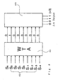
- the function of the WTA is such that the circuit outputs a value of 1 only to the output terminal corresponding to the smallest input, while the value is outputted to all other output terminals;
- Figure 4 shows the case in which S 3 has the smallest value among the 9 input signals. That is to say, only the output of the WTA corresponding to S 3 has a value of 1.
- This is inputted into address encoder 403, and a binary code corresponding to +3, for example, 0011, is outputted as the value of ⁇ x.
- a ROM with prescribed codes written thereinto may be employed as this address encoder, or alternatively, combined logical circuitry may be employed.
- S n and V n are, respectively, the input terminal and output terminal corresponding to the number n of WTA 401; circuitry identical to that of reference 501 is used with respect to each input.
- Reference 502 indicates a CMOS inverter; the common gate 503 thereof is placed in an electrically floating state by placing switches SW1 and SW2 in an OFF state.
- the 2 inputs S n and V R are capacitively coupled with floating gate 503 via capacitors having the same size.
- switch SW1 is closed.
- CMOS inverter 502 is biased at the point at which the input and output characteristics change the most rapidly, and V FG becomes equal to V DD /2.
- switch SW1 is placed in an OFF state, and the common gate 503 is placed in a floating state.
- V FG becomes V DD /2
- CMOS inverter 502 enters an ON state, the output thereof drops to 0 V, and if V FG is less than V DD /2, the inverter enters an OFF state, and the output thereof rises to V DD .
- Reference 504 indicates a 9 input NAND circuit; since the inputs thereof are all values of 1, the output 505 has a value of 0. By means of this, switch SW2 is placed in an OFF state.
- the WTA function is realized in the above manner.
- the circuitry of Figure 5 represents only 1 example of a WTA, and it is of course the case that circuits having other forms may be employed.
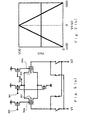
- Figure 6(a) is a circuit diagram, and V 1 and V 2 represent the two inputs thereof; these correspond to the input terminals for the A data and the B data.
- the operational principle of the present circuit will be explained using Figure 7.
- the state of each switch in the state in which a prescribed input voltage is applied to V 1 and V 2 is as shown in Figure 7(a).
- NMOS switches 601 and 602 are placed in an OFF state, and the gate electrodes 603a and 604a of NMOS transistors 603 and 604 are placed in a floating state ( Figure 7(b)).
- the switches 605a-d of the input portion are switched and the input voltages are switched, the potential of floating gates 603 and 604 become equal to V 2 - V 1 and V 1 - V 2 . If V 1 > V 2 , then V 2 - V 1 ⁇ 0, and the potential thereof is fixed at the diffusion potential (approximately -0.7 V) by means of the drain PN junction of the NMOS transistor 601 ( Figure 7(c)
- circuit of Figure 6 represents only one example; it is of course the case that any circuit may be employed insofar as it is a circuit which outputs a value proportional to
- Reference 801 indicates an A data series storing the t + ⁇ t data
- reference 802 indicates a B data series memory storing the t data.
- a concrete circuit diagram is shown in Figure 9.
- the wiring supplying the A data 801 and B data 802 to each cell is shown by, respectively, references 804 and 805 (the lines running in a diagonal direction) .
- the basic structure is identical to that of Figure 2, so that a detailed explanation thereof will be omitted here.
- Reference 806 corresponds to the source follower circuit 309, while reference 807 corresponds to the floating gate 305 thereof.
- Reference 808 indicates a WTA.
- the WTA circuit outputs a value of 1 only at the position of the input having the maximum value; concretely, a circuit such as that shown in, for example, Figure 11, may be employed.
- FIG. 9(a) is a circuit which is almost identical in principle to that of Figure 6(a); the chief differences thereof are that PMOS 903 and 904 are employed in place of NMOS 603 and 604, and the voltage becomes V DD when the gates 903a and 904a thereof are reset.
- Figure 9(b) which shows the characteristics of the V out thereof, shows characteristics in which 0 and V DD are inputted in a reversed manner (characteristics such that the graph appears to be turned upside down) and the circuit outputs the largest value (VDD) when V 1 and V 2 are in agreement, while when V 1 and V 2 are separated by the furthest amount, then the minimum value (0 V) is outputted. That is to say, as the data in each cell in Figure 8 become closer, the score becomes higher, and the value of S n becomes larger.
- FIG 10 shows the results of a simulation of the operation of the circuit of Figure 9 using a circuit simulator (HSPICE).
- RST indicates the control signal applied to terminal 905
- SFact indicates the control signal applied to terminal 906; output is obtainable when both of these are at the low (0 V) value. It can be seen that the circuit operated as expected.
- the circuit of Figure 11 is almost identical to that of Figure 5. There are 3 differences: the output inverter 506 of Figure 5 is removed, the NAND circuit is replaced by OR circuit 1101, and V R is initially set to 0 V, and is then ramped up from 0 to V DD . V n has a value of '1' only when S n has the largest value in the circuit.
- Figure 12 shows the results of a simulation of the circuit of Figure 8 using a circuit simulator (HSPICE).
- HSPICE circuit simulator
- SFinp indicates the input voltage into source follower circuit 806 and the like, or in other words, the potential wave form of floating gate 807 and the like
- SFout indicates the output wave form of the source follower.
- movement vectors were found using data representing the direct addition, by row or by column, of 2 dimensional image sensor data; however, image processing such as edge detection or the like may conducted in advance with respect to the 2 dimensional image data, and after that, the data may be added by row or by column.
- image processing such as edge detection or the like may conducted in advance with respect to the 2 dimensional image data, and after that, the data may be added by row or by column.
- this method improved the accuracy of detection.
- a method may be adopted in which one or other of these methods are appropriately selected, operations are conducted successively in which results are determined using both cases with the same hardware, and thus movement detection is conducted with higher accuracy.
- the result of the addition of 1 row or 1 column of pixel data corresponded to 1 datum; however, 2 or more rows, or two or more column of data may be added, and this may be made to correspond to 1 datum.
- a correlation operational circuit which only conducted operations which obtained the absolute value; however, other operations may be employed. For example, an operation which determines the largest value of A i and B i+n may be conducted, and the amount of movement may be determined by the minimum value of the total of these maximum values for each cell. Furthermore, this may be reversed, and the minimum values of A i and B i+n may determined, and the amount of movement found by finding the maximum total of the minimum values for each cells. Furthermore, a so-called matching operation may be conducted in which the output is VDD only when
- a further important point in the present invention is that it is not necessary that the t data be in perfect agreement with the t + ⁇ t data with respect to the pixel shift.
- the shift resulting in the relatively closest fit is found, so that even if an object moves while the form thereof is changed slightly, the amount of movement can be found without problem.
- FIG. 14 This is an operational circuit which accurately finds only the amount of movement of a moving object when the specified object is moving against a still background.
- Reference 1401 indicates an image sensor array, while reference 1402 indicates a ⁇ x detection circuit; these are identical to those described in Figure 1.
- a new circuit block 1403 is added.
- References 1404 - 1406 indicate memories which store sum signals in the columnar direction of the image sensor, that is to say, the x axis projection data; these memories are used for the data of the 3 time frames such that memory 1404 stores the t - ⁇ t data, memory 1405 stores the t data, and memory 1406 stores the t + ⁇ t data.
- Reference 1407 indicates an absolute value operational circuit; this calculates the absolute value of the difference of the t - ⁇ t data and the t data, and the absolute value of the difference between the t data and the t + ⁇ t data, and provides these as the A data series and B data series to the ⁇ x detection circuit.
- the circuit shown in Figure 6 may be employed as this circuit.
- Figure 15(a) depicts a balloon moving over a building. Only the balloon moves, and it moves to the right.
- the x axis projection data of the data of (a) are as shown in Figure 15(b), and the data after ⁇ t are as shown in Figure 15(c), and as the background is incorporated in these data, it is extremely difficult to determine the amount of movement using a pixel shift.
- the absolute of the difference of both is obtained as in Figure 15(e)
- the background is made stationary, so that this is canceled out and disappears.
- a fourth embodiment of the present invention is shown in Figure 16.
- This circuit executes a SEARCH (N, M) command with respect to data series A 1 - A 8 and B 1 - B 8 comprising 2 groups of 8 data. That is to say, the circuit takes a number of continuous data M from the position having the ordinal number N in the A data series, and determines at what position in the B data the best agreement is found. For example, in this embodiment, if M is the values from 4 - 6, then N takes a value within a range of 1 - (8 - M).
- References 1601 and 1602 indicate memories storing, respectively, the A data and the B data
- reference 1603 indicates a circuit group identical to 203 in Figure 2; each correlation operational circuit cell is identical to those in the first and second embodiment, and any type of circuit may be employed.
- the A data and the B data are supplied to each cell along the lines shown, respectively, by the arrows and the dotted lines.
- the sixth data on the right hand side A 3 , A 4 ,- A 8 and the sixth data B 1 , B 2 , - B 6 are supplied to the row 1604.
- This figure shows the structure related to the cells of row 1604 in Figure 16. Since only 6 cells are incorporated in 1604, this row has 2 fewer cells than the largest row 1605, which has 8 cells. Accordingly, dummy capacitors 1701 and 1702 are added so that the total reaches 8, and the input terminal thereof fall to the ground potential. By means of this, it is possible to set the total capacity value as seen from the floating gate 1703 to the same value in all rows. Furthermore, the minimum value of M of the search (N, M) is 4, so that there are cases in which only 4 cells are employed. In this case, switches 1704 and 1705, for example, may be set to the ground side, and cells 1706 and 1707 may be cut off.
- the cells 1708 - 1711 which are necessary for the operation may have the cell outputs thereof connected to capacitors via switches, and the output thereof may be transmitted to floating gate 1703. By doing this, it is possible to conduct size comparisons with a constant value for the gain of the source follower circuit 1712.
- Figure 18 illustrates a different invention for cutting off unnecessary cells.
- no dummy capacitors are employed.
- the switches 1807 and 1808 are thrown to the left, and connected to the output of source follower 1809.
- the value of V out is essentially equal to the voltage V FG of floating gate 1810, so that no voltage is applied to the two sides of capacitors 1811 and 1812 and no charge builds up. This is the same as if capacitors 1811 and 1812 were not present, and this is essentially equivalent to cutting these capacitors off completely from the floating gate 1810.
- the source follower operates constantly with the largest gain even if the number of cells is small, so that detection of the degree of movement can be conducted with a high degree of accuracy.
- Figure 19 shows an example of the operation of the circuitry when the SEARCH (N, M) command is actually executed.
- Figure 19(a) shows, for example, SEARCH (3,4); the data A 3 , A 4 , A 5 , and A 6 (1902) within the A data memory 1901 are compared with the B data 1903. At this time, only those correlation operational cells within the box indicated by the heavy line 1904 are employed, so that control must be conducted which ignores the output of the other cells.
- rows 1904a, 1904b, and the like it is necessary to cut off unnecessary cells using the method shown in Figure 17 and 18. Furthermore, in other rows, for example, in rows 1905a, 1905b, and the like, there is no need to input the operational results S -4 , S -3 , and the like into the WTA (for example, 401, 808, or the like), so that the input into the WTA may be fixed at a standard value of 0 V, V DD , or the like. If the WTA determines the input having the smallest value as shown in Figure 5, then the inputs may be set to V DD , while if the WTA determines the input having the largest value as in Figure 11, these inputs may be set to 0 V.
- Figure 19(b) shows the case of the command SEARCH (1, 6); the cells outside the box marked with the heavy line may be cut off using control identical to that described above.
- data series may be used as the two groups of data which are obtained from, for example, a 1 dimensional image sensor (an image sensor in which a plurality of pixels are arranged in a series).
- incident rays may be split in two directions using a micro lens, and these may be captured by different 1 dimensional image sensors, and operations may be conducted using the data thereof as the two groups of data series.
- the dislocation and the focal point may be detected and tight adjustment of the photo lens may be conducted, and thereby, an autofocus function may be realized.
- Figure 20 shows a fifth embodiment of the present invention.
- a SEARCH (N, M) command is executed with respect to two types of data series A and B.
- Reference 2001 indicates an A data series memory, while reference 2002 indicates a B data series memory.
- Reference 2003 indicates an analog data shift register; here, this has the function of shifting the data to the left one datum at a time.
- Reference 2004 indicates 6 operational circuits arranged in a series, which have the same function as those of Figure 2(b). The process of executing a SEARCH (3, 4) command will be explained hereinbelow.
- the entire A data series of memory 2001 is transferred to shift register 2003, and these are shifted 3 places to the left, and stored in operational circuit 2004.
- the B data series are entered into shift register 2003, and are then transferred to operational circuits 2004 without being shifted.
- the data A 3 , A 4 , A 5 , A 6 , A 7 , and A 8 and the data B 1 , B 2 , B 3 , B 4 , B 5 , and B 6 are incorporated into the cells C 1 , C 2 , ..., C 6 of the operational circuit, and if the operation
- (n -2) is conducted, the output is transferred to floating gate 2006 of source follower circuit 2005 via capacitive coupling. At this time, 4 comparator operations are necessary, so that it is necessary to cut off the output of C 5 and C 6 .
- the technology of Figure 17 and 18 is used to do this.
- the V out obtained in this manner is S -2 .
- S n is obtained in a successive time series; this may be temporarily stored in an analog memory, and the value of n giving the minimum value may be specified using a WTA such as that shown, for example, in Figure 5.
- size comparisons may be conducted with respect to the successively appearing values of S n , and the value of n giving the smaller value may be constantly followed. If the present embodiment of the present invention is employed, it is possible to execute operations which find the degree of agreement using smaller scale circuitry.
- a shift register 2003 was employed here; however, a switch matrix, for example, may be employed, and the prescribed data series may be selected by means of switches and conducted to operational circuit 2004.
- analog memory elements were not specified; however, it is of course the case that any technology may be used for these.
- analog data may be stored as a charge in capacitors, and these may be read out by a source follower circuit.
- the data may be stored in the base capacity of bi-polar transistors, and may be read out by an emitter follower circuit.
- storage may be conducted as digital data, or a many-valued memory (for example, that of R. Au, et, al., ISSCC' 94 Digest of Technical Papers, pp. 270 - 271) maybe employed.
- image sensor it is of course the case that any technology may be employed, such as, for example, a CCD (charge conduction device), a MOS image sensor, a bi-polar image sensor, or the like.
- the circuit of the present invention can be realized using extremely small scale circuitry, so that it may be integrated together with a 1 dimensional image sensor or 2 dimensional image sensor on the same chip, and is thus optimal for data processing in which image data are captured and operations are instantly executed with respect to these data. It is especially suited to conducting such operations. However, if the image sensor is on a separate chip, this does not depart from the essential features of the present invention. After 2 dimensional image data have been subjected one by one to A/D conversion, and incorporated in a frame memory comprising DRAM sets or the like, processing may be conducted using the circuit of the present invention.
- the D/A conversion employs a ratio having sizes in which the capacity values are multiples of 2, such as 1, 2, 4, 8, ..., and the conversion takes advantage of the capacitive coupling with the floating gate. That is to say, D/A conversion may be easily conducted at this floating gate as the output of a controlled source follower circuit.
- this floating gate may be the floating gate (603a, 604a) of, for example, an absolute value operational circuit ( Figure 6(a)). If this is done, there is no gain drop as a result of the source follower, and it is possible to execute operations having a higher degree of accuracy.
- circuits of the present invention may be directly integrated on a DRAM chip comprising frame memory, or may be placed in one portion of a microprocessor chip. That is to say, the circuitry of the present invention may be combined as one block within a purely digital circuit, and in the exclusively digital operations, may be employed as an acceleration engine with respect to special jobs which aids those operations requiring an enormous amount of time.
Claims (16)
- Halbleiteroperationsschaltkreis, der eine vorherbestimmte Operation ausführt, und zwar bezüglich einer ersten Signalfolge von Signalen A1, A2, ..., AN-1, AN, wobei N eine positive Ganzzahl von N Signalen ist, die von 1 bis N nummeriert sind, und bezüglich einer zweiten Signalfolge von Signalen B1, B2, ..., BM-1, BM, wobei M eine positive Ganzzahl von M Signalen ist, die von 1 bis M nummeriert sind, wobei der Schaltkreis Folgendes umfasst: eine Vielzahl von ersten Operationsschaltkreisen zur Ausführung einer vorherbestimmten Operation bezüglich Ai und Bi+n, wobei i eine positive Ganzzahl und n eine positive oder negative Ganzzahl ist und 1 ≤ i ≤ n und 1 ≤ i + n ≤ M ist, und zur Erzeugung eines Ausgabesignals Ci,n, mindestens einen zweiten Operationsschaltkreis zur Erzeugung der Summe Sn eines Teils oder der Gesamtheit der Ausgabesignale der ersten Operationsschaltkreise bezüglich eines vorherbestimmten Wertes von n, wobei i unterschiedliche Werte aufweist, oder zur Erzeugung eines vorherbestimmten Signals Tn, das von der Summe Sn bestimmt wird, und einen dritten Operationsschaltkreis zur Ermittlung des Wertes von Sn oder Tn bezüglich einer Vielzahl verschiedener n-Werte und zur Bestimmung des n-Wertes, für den der Höchst- oder Mindestwert von Sn oder Tn gegeben ist.
- Halbleiteroperationsschaltkreis nach Anspruch 1, wobei die ersten Operationsschaltkreise die Funktion der Erzeugung eines Spannungssignals Ci,n übernehmen, das zusammen mit dem absoluten Wert von Ai - Bi+n monoton zunimmt.
- Halbleiteroperationsschaltkreis nach Anspruch 1, wobei die ersten Operationsschaltkreise die Funktion der Erzeugung eines Spannungssignals Ci,n übernehmen, das zusammen mit dem absoluten Wert von Ai - Bi+n monoton abnimmt.
- Halbleiteroperationsschaltkreis nach Anspruch 1 bis 3, wobei die ersten Operationsschaltkreise mit einem Paar MOS-Transistoren versehen sind, die Kanäle desselben Leitfähigkeitstyps aufweisen, und Quellenelektroden dieser Transistoren miteinander verbunden sind und eine Anschlussklemme bilden, die eine Ausgangsspannung erzeugt.
- Halbleiteroperationsschaltkreis nach Anspruch 4, wobei ein Mittel vorgesehen ist, das Torelektroden des Paars MOS-Transistoren in einen elektrisch ungeerdeten Zustand versetzt.
- Halbleiteroperationsschaltkreis nach Anspruch 1, wobei die ersten Operationsschaltkreise die Funktion der Ausgabe eines Spannungssignals übemehmen, das einen hohen Pegel aufweist, der einen logischen Wert von "1" darstellt, wenn der Wert Ai - Bi+n kleiner als ein vorherbestimmter Wert ist, und ein Spannungssignal ausgibt, das einen niedrigen Pegel aufweist, der einen logischen Wert von "0" in anderen Fällen darstellt.
- Halbleiteroperationsschaltkreis nach Anspruch 1, wobei die ersten Operationsschaltkreise die Funktion der Ausgabe eines Spannungssignals übernehmen, das einen niedrigen Pegel aufweist, der einen logischen Wert von "0" darstellt, wenn der Wert Ai - Bi+n kleiner als ein vorherbestimmter Wert ist, und ein Spannungssignal ausgibt, das einen hohen Pegel aufweist, der einen logischen Wert von "1" in anderen Fällen darstellt.
- Halbleiteroperationsschaltkreis nach einem der Ansprüche 1 bis 7, wobei der zweite Operationsschaltkreis mit einer ersten Elektrode in einem elektrisch ungeerdeten Zustand versehen ist, die über einen Kondensator mit Ausgangselektroden der ersten Operationsschaltkreise gekoppelt ist, und weiterhin mindestens einen MOS-Transistor umfasst, dessen Schalt-Sperr-Zustand von der ersten Elektrode gesteuert wird.
- Halbleiteroperationsschaltkreis nach einem der Ansprüche 1 bis 8, der eine zweite Schaltkreisgruppe umfasst, die eine Vielzahl von ersten Schaltkreisgruppen umfasst, in denen die ersten Operationsschaltkreise linear angeordnet sind, wobei ein Signal der ersten Signalfolge und ein Signal der zweiten Signalfolge in unterschiedlichen Kombinationen an. entsprechende erste Operationsschaltkreise in der zweiten Schaltkreisgruppe angelegt werden.
- Halbleiteroperationsschaltkreis nach Anspruch 9, wobei der zweite Operationsschaltkreis jeder ersten Schaltkreisgruppe hinzugefügt ist.
- Halbleiteroperationsschaltkreis nach einem der Ansprüche 1 bis 8, wobei ein Mittel zum Leiten einer Vielzahl vorgeschriebener verbundener Signalfolgen von einem ersten Signal aus der ersten oder zweiten Signalfolge zur Vielzahl von ersten Operationsschaltkreisen vorgesehen ist, wobei eine Vielzahl von vorgeschriebenen verbundenen Signalfolgen von einem zweiten Signal zur Vielzahl der ersten Operationsschaltkreise geleitet wird, nachdem die vorgeschriebenen Signale Sn oder Tn berechnet wurden und die Signale Sn oder Tn hinsichtlich unterschiedlicher Werte von n berechnet wurden.
- Halbleiteroperationsschaltkreis nach einem der Ansprüche 1 bis 11, wobei eine Vielzahl von lichtempfindlichen Halbleitersensoren auf demselben Halbleitersubstrat integriert ist.
- Halbleiteroperationsschaltkreis nach einem der Ansprüche 1 bis 12, wobei mindestens eine Sensorreihe vorgesehen ist, die eine Vielzahl von geradlinig verdrahteten, lichtempfindlichen Halbleitersensoren umfasst, und mindestens ein Abschnitt der Signalfolge, die von der Sensorreihe erhalten wird, oder eine Signalfolge, die aus der Ausführung der vorgeschriebenen Operationsverarbeitung derselben resultiert, die erste oder zweite Signalfolge bildet.
- Halbleiteroperationsschaltkreis nach einem der Ansprüche 1 bis 12, wobei eine Sensorgruppe vorgesehen ist, in der lichtempfindliche Halbteitersensoren in Form einer zweidimensionalen Matrix angeordnet sind, und Signale, die aus der Addition von Signalen, die von den lichtempfindlichen Sensoren erhalten wurden, oder Signale, die aus der Ausführung der vorgeschriebenen Operationen an denselben resultieren und in Spaltenrichtung für jede Spalte addiert werden und/oder in Zeilenrichtung für jede Zeile addiert werden, einen Teil der ersten oder zweiten Signalfolge bilden.
- Halbleiteroperationsschaltkreis nach einem der Ansprüche 1 bis 14, wobei ein Mittel zur Ausführung einer vorgeschriebenen Operationsverarbeitung hinsichtlich Bilddaten vorgesehen ist, die zu 3 fortlaufenden Zeiten t1, t2 und t3 eingegliedert werden, und ein Mittel zur Erzeugung der ersten und zweiten Signalfolge vorgesehen ist, indem bezüglich Signalen, die Bilddaten zu den Zeiten t1, t2 und t3 entsprechen, an denen eine vorgeschriebene Operationsverarbeitung ausgeführt wurde, der absolute Wert der Differenz zwischen den Signalen der Zeiten t1 und t2 bestimmt wird, und zur Erzeugung einer zweiten oder ersten Signalfolge durch Ermitteln des absoluten Wertes der Differenz zwischen den Signalen der Zeiten t2 und t3.
- Halbleiteroperationsschaltkreis nach Anspruch 15, wobei die vorgeschriebene Operationsverarbeitung eine Verarbeitung durchführt, bei der Signale der zweidimensionalen Anordnung der lichtempfindlichen Sensoren, die in Form einer Matrix angeordnet sind, zeilenweise und/oder spaltenweise addiert werden.
Applications Claiming Priority (4)
| Application Number | Priority Date | Filing Date | Title |
|---|---|---|---|
| JP10046095 | 1995-03-31 | ||
| JP100460/95 | 1995-03-31 | ||
| JP10046095 | 1995-03-31 | ||
| PCT/JP1996/000885 WO1996030854A1 (fr) | 1995-03-31 | 1996-04-01 | Logique de calcul a semi-conducteur |
Publications (3)
| Publication Number | Publication Date |
|---|---|
| EP0820030A1 EP0820030A1 (de) | 1998-01-21 |
| EP0820030A4 EP0820030A4 (de) | 1999-11-03 |
| EP0820030B1 true EP0820030B1 (de) | 2003-07-02 |
Family
ID=14274529
Family Applications (1)
| Application Number | Title | Priority Date | Filing Date |
|---|---|---|---|
| EP96907743A Expired - Lifetime EP0820030B1 (de) | 1995-03-31 | 1996-04-01 | Halbleiterfunktionsschaltung |
Country Status (4)
| Country | Link |
|---|---|
| US (1) | US5956434A (de) |
| EP (1) | EP0820030B1 (de) |
| DE (1) | DE69628919T2 (de) |
| WO (1) | WO1996030854A1 (de) |
Families Citing this family (8)
| Publication number | Priority date | Publication date | Assignee | Title |
|---|---|---|---|---|
| JPH10224224A (ja) * | 1997-02-03 | 1998-08-21 | Sunao Shibata | 半導体演算装置 |
| JPH10283793A (ja) * | 1997-02-06 | 1998-10-23 | Sunao Shibata | 半導体回路 |
| JPH10257352A (ja) | 1997-03-15 | 1998-09-25 | Sunao Shibata | 半導体演算回路 |
| JPH10260817A (ja) | 1997-03-15 | 1998-09-29 | Sunao Shibata | 半導体演算回路及びデ−タ処理装置 |
| JPH1196276A (ja) | 1997-09-22 | 1999-04-09 | Sunao Shibata | 半導体演算回路 |
| SI2513599T1 (sl) * | 2009-12-18 | 2015-08-31 | Vito Nv (Vlaamse Instelling Voor Technologisch Onderzoek Nv) | Georeferenciranje multispektralnih podatkov |
| JP5501194B2 (ja) * | 2010-10-29 | 2014-05-21 | 株式会社キーエンス | 画像計測装置、画像計測方法及びコンピュータプログラム |
| US8588525B1 (en) * | 2011-11-17 | 2013-11-19 | Google Inc. | Transformation invariant media matching |
Family Cites Families (4)
| Publication number | Priority date | Publication date | Assignee | Title |
|---|---|---|---|---|
| FR2659817B1 (fr) * | 1990-03-13 | 1992-05-29 | Thomson Csf | Dispositif de reconnaissance de sequences dans un signal multidimensionnel. |
| FR2670923A1 (fr) * | 1990-12-21 | 1992-06-26 | Philips Lab Electronique | Dispositif de correlation. |
| EP0497586A3 (en) * | 1991-01-31 | 1994-05-18 | Sony Corp | Motion detection circuit |
| US5497343A (en) * | 1993-08-05 | 1996-03-05 | Hyundai Electronics America | Reducing the number of carry-look-ahead adder stages in high-speed arithmetic units, structure and method |
-
1996
- 1996-04-01 DE DE69628919T patent/DE69628919T2/de not_active Expired - Fee Related
- 1996-04-01 US US08/930,548 patent/US5956434A/en not_active Expired - Fee Related
- 1996-04-01 EP EP96907743A patent/EP0820030B1/de not_active Expired - Lifetime
- 1996-04-01 WO PCT/JP1996/000885 patent/WO1996030854A1/ja active IP Right Grant
Also Published As
| Publication number | Publication date |
|---|---|
| DE69628919T2 (de) | 2004-06-03 |
| EP0820030A1 (de) | 1998-01-21 |
| WO1996030854A1 (fr) | 1996-10-03 |
| EP0820030A4 (de) | 1999-11-03 |
| DE69628919D1 (de) | 2003-08-07 |
| US5956434A (en) | 1999-09-21 |
Similar Documents
| Publication | Publication Date | Title |
|---|---|---|
| EP0709794B1 (de) | Halbleiterschaltung und ihre Anwendung in einer Operationsschaltung, einem Signalwandler und einem Signalverarbeitungssystem | |
| EP0725357B1 (de) | Halbleiteranordnung, Schaltung mit dieser Anordnung, und Korrelationsrechner, Signalwandler und Signalverarbeitungssystem, in welchem die Schaltung angewandt wird | |
| US11082653B2 (en) | Image sensor and pixel array which generate a pixel signal based on a plurality of pixels, and operation method of the image sensor | |
| EP0709792B1 (de) | Halbleiterschaltung und ihre Anwendung in einer Operationsschaltung, einem Signalwandler und einem Signalverarbeitungssystem | |
| EP0820030B1 (de) | Halbleiterfunktionsschaltung | |
| US5917960A (en) | Image correlator, an image processing apparatus using the same, and a signal adder used in the image correlator | |
| KR0172196B1 (ko) | 반도체 디바이스 및 산술 논리 장치, 신호 변환기 및 이를 이용한 신호 처리 시스템 | |
| US7279668B2 (en) | Sequential read-out method and system that employs a single amplifier for multiple columns | |
| EP1435588A1 (de) | Bilderfassungsvorrichtung | |
| US20220285413A1 (en) | Image sensor | |
| US11233962B2 (en) | Image sensor and pixel array which operate based on a clamp voltage and a selection voltage, and operation method of the image sensor | |
| EP1076310A1 (de) | Rechenschaltung, Recheneinrichtung und Halbleiter-Rechenschaltung | |
| KR100224557B1 (ko) | 반도체 장치, 연산 장치, 신호 변환기, 및 반도체 장치를 이용한 신호 처리시스템 | |
| US5847669A (en) | Semiconductor device and signal processing system using the same | |
| JPH08204562A (ja) | 半導体装置、及びそれを用いた半導体回路、相関演算装置、a/d変換器、d/a変換器及び信号処理システム | |
| US6667767B1 (en) | Image sensor for offsetting threshold voltage of a transistor in a source follower | |
| US20180295306A1 (en) | Image sensors with diagonal readout | |
| US6606119B1 (en) | Semiconductor arithmetic circuit | |
| EP0823684B1 (de) | Halbleiterfunktionsschaltung | |
| US6049235A (en) | Semiconductor device, signal processing system using the same, and calculation method therefor | |
| US5008696A (en) | Phase difference detecting apparatus | |
| US4945377A (en) | Phase difference detecting apparatus | |
| JPH09274133A (ja) | 相関器と画像相関器、信号加算器、画像処理回路及びこれらを用いた自動焦点カメラ | |
| US20230179884A1 (en) | Image sensor device and operation method thereof | |
| JPH01229212A (ja) | 位相差検出装置 |
Legal Events
| Date | Code | Title | Description |
|---|---|---|---|
| PUAI | Public reference made under article 153(3) epc to a published international application that has entered the european phase |
Free format text: ORIGINAL CODE: 0009012 |
|
| 17P | Request for examination filed |
Effective date: 19971024 |
|
| AK | Designated contracting states |
Kind code of ref document: A1 Designated state(s): DE GB NL |
|
| A4 | Supplementary search report drawn up and despatched |
Effective date: 19990920 |
|
| AK | Designated contracting states |
Kind code of ref document: A4 Designated state(s): DE GB NL |
|
| RIC1 | Information provided on ipc code assigned before grant |
Free format text: 6G 06G 7/12 A, 6G 06G 7/26 B |
|
| GRAH | Despatch of communication of intention to grant a patent |
Free format text: ORIGINAL CODE: EPIDOS IGRA |
|
| GRAH | Despatch of communication of intention to grant a patent |
Free format text: ORIGINAL CODE: EPIDOS IGRA |
|
| GRAH | Despatch of communication of intention to grant a patent |
Free format text: ORIGINAL CODE: EPIDOS IGRA |
|
| GRAA | (expected) grant |
Free format text: ORIGINAL CODE: 0009210 |
|
| AK | Designated contracting states |
Designated state(s): DE GB NL |
|
| REG | Reference to a national code |
Ref country code: GB Ref legal event code: FG4D |
|
| REF | Corresponds to: |
Ref document number: 69628919 Country of ref document: DE Date of ref document: 20030807 Kind code of ref document: P |
|
| PG25 | Lapsed in a contracting state [announced via postgrant information from national office to epo] |
Ref country code: GB Free format text: LAPSE BECAUSE OF NON-PAYMENT OF DUE FEES Effective date: 20040401 |
|
| PLBE | No opposition filed within time limit |
Free format text: ORIGINAL CODE: 0009261 |
|
| STAA | Information on the status of an ep patent application or granted ep patent |
Free format text: STATUS: NO OPPOSITION FILED WITHIN TIME LIMIT |
|
| 26N | No opposition filed |
Effective date: 20040405 |
|
| PG25 | Lapsed in a contracting state [announced via postgrant information from national office to epo] |
Ref country code: NL Free format text: LAPSE BECAUSE OF NON-PAYMENT OF DUE FEES Effective date: 20041101 |
|
| GBPC | Gb: european patent ceased through non-payment of renewal fee | ||
| NLV4 | Nl: lapsed or anulled due to non-payment of the annual fee |
Effective date: 20041101 |
|
| PGFP | Annual fee paid to national office [announced via postgrant information from national office to epo] |
Ref country code: DE Payment date: 20050524 Year of fee payment: 10 |
|
| PG25 | Lapsed in a contracting state [announced via postgrant information from national office to epo] |
Ref country code: DE Free format text: LAPSE BECAUSE OF NON-PAYMENT OF DUE FEES Effective date: 20061101 |