EP0818557B1 - Procédé et installation pour la formation d'un revêtement sur un substrat - Google Patents
Procédé et installation pour la formation d'un revêtement sur un substrat Download PDFInfo
- Publication number
- EP0818557B1 EP0818557B1 EP97870100A EP97870100A EP0818557B1 EP 0818557 B1 EP0818557 B1 EP 0818557B1 EP 97870100 A EP97870100 A EP 97870100A EP 97870100 A EP97870100 A EP 97870100A EP 0818557 B1 EP0818557 B1 EP 0818557B1
- Authority
- EP
- European Patent Office
- Prior art keywords
- substrate
- coating
- zone
- process according
- reaction zone
- Prior art date
- Legal status (The legal status is an assumption and is not a legal conclusion. Google has not performed a legal analysis and makes no representation as to the accuracy of the status listed.)
- Expired - Lifetime
Links
- 239000000758 substrate Substances 0.000 title claims abstract description 68
- 238000000576 coating method Methods 0.000 title claims abstract description 41
- 239000011248 coating agent Substances 0.000 title claims abstract description 40
- 238000000034 method Methods 0.000 title claims abstract description 38
- 238000006243 chemical reaction Methods 0.000 claims abstract description 52
- 238000000151 deposition Methods 0.000 claims abstract description 51
- 230000008021 deposition Effects 0.000 claims abstract description 41
- 150000002500 ions Chemical class 0.000 claims abstract description 23
- 229910052751 metal Inorganic materials 0.000 claims abstract description 18
- 239000002184 metal Substances 0.000 claims abstract description 18
- 150000001875 compounds Chemical class 0.000 claims abstract description 17
- 238000001704 evaporation Methods 0.000 claims description 10
- 230000008020 evaporation Effects 0.000 claims description 10
- 238000004544 sputter deposition Methods 0.000 claims description 9
- ATJFFYVFTNAWJD-UHFFFAOYSA-N Tin Chemical compound [Sn] ATJFFYVFTNAWJD-UHFFFAOYSA-N 0.000 claims description 6
- 239000002245 particle Substances 0.000 claims description 6
- 238000009833 condensation Methods 0.000 claims description 4
- 230000005494 condensation Effects 0.000 claims description 4
- 238000007738 vacuum evaporation Methods 0.000 claims description 4
- 239000000919 ceramic Substances 0.000 claims description 3
- 230000005284 excitation Effects 0.000 claims 1
- 239000007943 implant Substances 0.000 claims 1
- 230000001939 inductive effect Effects 0.000 claims 1
- 239000010410 layer Substances 0.000 claims 1
- 239000002344 surface layer Substances 0.000 claims 1
- 238000009434 installation Methods 0.000 abstract description 12
- 229910045601 alloy Inorganic materials 0.000 abstract description 3
- 239000000956 alloy Substances 0.000 abstract description 3
- 239000004065 semiconductor Substances 0.000 abstract description 3
- 238000005468 ion implantation Methods 0.000 abstract 1
- 239000007789 gas Substances 0.000 description 16
- 239000011521 glass Substances 0.000 description 9
- 238000002513 implantation Methods 0.000 description 9
- 230000015572 biosynthetic process Effects 0.000 description 8
- XKRFYHLGVUSROY-UHFFFAOYSA-N argon Substances [Ar] XKRFYHLGVUSROY-UHFFFAOYSA-N 0.000 description 5
- QCWXUUIWCKQGHC-UHFFFAOYSA-N Zirconium Chemical compound [Zr] QCWXUUIWCKQGHC-UHFFFAOYSA-N 0.000 description 4
- -1 argon ions Chemical class 0.000 description 4
- 229910052738 indium Inorganic materials 0.000 description 4
- APFVFJFRJDLVQX-UHFFFAOYSA-N indium atom Chemical compound [In] APFVFJFRJDLVQX-UHFFFAOYSA-N 0.000 description 4
- 229910052726 zirconium Inorganic materials 0.000 description 4
- 229910000831 Steel Inorganic materials 0.000 description 3
- 229910052786 argon Inorganic materials 0.000 description 3
- 239000007788 liquid Substances 0.000 description 3
- 239000010959 steel Substances 0.000 description 3
- IJGRMHOSHXDMSA-UHFFFAOYSA-N Atomic nitrogen Chemical compound N#N IJGRMHOSHXDMSA-UHFFFAOYSA-N 0.000 description 2
- 239000003153 chemical reaction reagent Substances 0.000 description 2
- 238000011109 contamination Methods 0.000 description 2
- 238000005034 decoration Methods 0.000 description 2
- 238000006073 displacement reaction Methods 0.000 description 2
- 239000011532 electronic conductor Substances 0.000 description 2
- 239000005357 flat glass Substances 0.000 description 2
- 238000004519 manufacturing process Methods 0.000 description 2
- 239000004033 plastic Substances 0.000 description 2
- 229920003023 plastic Polymers 0.000 description 2
- 238000005546 reactive sputtering Methods 0.000 description 2
- ZVWKZXLXHLZXLS-UHFFFAOYSA-N zirconium nitride Chemical compound [Zr]#N ZVWKZXLXHLZXLS-UHFFFAOYSA-N 0.000 description 2
- 229910001209 Low-carbon steel Inorganic materials 0.000 description 1
- 239000004698 Polyethylene Substances 0.000 description 1
- 239000004743 Polypropylene Substances 0.000 description 1
- RTAQQCXQSZGOHL-UHFFFAOYSA-N Titanium Chemical compound [Ti] RTAQQCXQSZGOHL-UHFFFAOYSA-N 0.000 description 1
- NRTOMJZYCJJWKI-UHFFFAOYSA-N Titanium nitride Chemical compound [Ti]#N NRTOMJZYCJJWKI-UHFFFAOYSA-N 0.000 description 1
- 229910052782 aluminium Inorganic materials 0.000 description 1
- XAGFODPZIPBFFR-UHFFFAOYSA-N aluminium Chemical compound [Al] XAGFODPZIPBFFR-UHFFFAOYSA-N 0.000 description 1
- QVGXLLKOCUKJST-UHFFFAOYSA-N atomic oxygen Chemical compound [O] QVGXLLKOCUKJST-UHFFFAOYSA-N 0.000 description 1
- 239000002826 coolant Substances 0.000 description 1
- 238000001816 cooling Methods 0.000 description 1
- 230000003247 decreasing effect Effects 0.000 description 1
- 238000005516 engineering process Methods 0.000 description 1
- 230000004927 fusion Effects 0.000 description 1
- 239000011261 inert gas Substances 0.000 description 1
- 229910001338 liquidmetal Inorganic materials 0.000 description 1
- 238000001755 magnetron sputter deposition Methods 0.000 description 1
- 150000004767 nitrides Chemical class 0.000 description 1
- 229910052757 nitrogen Inorganic materials 0.000 description 1
- 239000001301 oxygen Substances 0.000 description 1
- 229910052760 oxygen Inorganic materials 0.000 description 1
- 230000000149 penetrating effect Effects 0.000 description 1
- 239000002985 plastic film Substances 0.000 description 1
- 229920006255 plastic film Polymers 0.000 description 1
- 229920000573 polyethylene Polymers 0.000 description 1
- 229920001155 polypropylene Polymers 0.000 description 1
- 239000007921 spray Substances 0.000 description 1
- 229910052719 titanium Inorganic materials 0.000 description 1
- 239000010936 titanium Substances 0.000 description 1
- 230000009466 transformation Effects 0.000 description 1
- 238000000844 transformation Methods 0.000 description 1
Images

Classifications
-
- C—CHEMISTRY; METALLURGY
- C23—COATING METALLIC MATERIAL; COATING MATERIAL WITH METALLIC MATERIAL; CHEMICAL SURFACE TREATMENT; DIFFUSION TREATMENT OF METALLIC MATERIAL; COATING BY VACUUM EVAPORATION, BY SPUTTERING, BY ION IMPLANTATION OR BY CHEMICAL VAPOUR DEPOSITION, IN GENERAL; INHIBITING CORROSION OF METALLIC MATERIAL OR INCRUSTATION IN GENERAL
- C23C—COATING METALLIC MATERIAL; COATING MATERIAL WITH METALLIC MATERIAL; SURFACE TREATMENT OF METALLIC MATERIAL BY DIFFUSION INTO THE SURFACE, BY CHEMICAL CONVERSION OR SUBSTITUTION; COATING BY VACUUM EVAPORATION, BY SPUTTERING, BY ION IMPLANTATION OR BY CHEMICAL VAPOUR DEPOSITION, IN GENERAL
- C23C14/00—Coating by vacuum evaporation, by sputtering or by ion implantation of the coating forming material
- C23C14/22—Coating by vacuum evaporation, by sputtering or by ion implantation of the coating forming material characterised by the process of coating
- C23C14/56—Apparatus specially adapted for continuous coating; Arrangements for maintaining the vacuum, e.g. vacuum locks
- C23C14/562—Apparatus specially adapted for continuous coating; Arrangements for maintaining the vacuum, e.g. vacuum locks for coating elongated substrates
-
- C—CHEMISTRY; METALLURGY
- C23—COATING METALLIC MATERIAL; COATING MATERIAL WITH METALLIC MATERIAL; CHEMICAL SURFACE TREATMENT; DIFFUSION TREATMENT OF METALLIC MATERIAL; COATING BY VACUUM EVAPORATION, BY SPUTTERING, BY ION IMPLANTATION OR BY CHEMICAL VAPOUR DEPOSITION, IN GENERAL; INHIBITING CORROSION OF METALLIC MATERIAL OR INCRUSTATION IN GENERAL
- C23C—COATING METALLIC MATERIAL; COATING MATERIAL WITH METALLIC MATERIAL; SURFACE TREATMENT OF METALLIC MATERIAL BY DIFFUSION INTO THE SURFACE, BY CHEMICAL CONVERSION OR SUBSTITUTION; COATING BY VACUUM EVAPORATION, BY SPUTTERING, BY ION IMPLANTATION OR BY CHEMICAL VAPOUR DEPOSITION, IN GENERAL
- C23C14/00—Coating by vacuum evaporation, by sputtering or by ion implantation of the coating forming material
- C23C14/06—Coating by vacuum evaporation, by sputtering or by ion implantation of the coating forming material characterised by the coating material
- C23C14/0641—Nitrides
-
- C—CHEMISTRY; METALLURGY
- C23—COATING METALLIC MATERIAL; COATING MATERIAL WITH METALLIC MATERIAL; CHEMICAL SURFACE TREATMENT; DIFFUSION TREATMENT OF METALLIC MATERIAL; COATING BY VACUUM EVAPORATION, BY SPUTTERING, BY ION IMPLANTATION OR BY CHEMICAL VAPOUR DEPOSITION, IN GENERAL; INHIBITING CORROSION OF METALLIC MATERIAL OR INCRUSTATION IN GENERAL
- C23C—COATING METALLIC MATERIAL; COATING MATERIAL WITH METALLIC MATERIAL; SURFACE TREATMENT OF METALLIC MATERIAL BY DIFFUSION INTO THE SURFACE, BY CHEMICAL CONVERSION OR SUBSTITUTION; COATING BY VACUUM EVAPORATION, BY SPUTTERING, BY ION IMPLANTATION OR BY CHEMICAL VAPOUR DEPOSITION, IN GENERAL
- C23C14/00—Coating by vacuum evaporation, by sputtering or by ion implantation of the coating forming material
- C23C14/06—Coating by vacuum evaporation, by sputtering or by ion implantation of the coating forming material characterised by the coating material
- C23C14/08—Oxides
-
- C—CHEMISTRY; METALLURGY
- C23—COATING METALLIC MATERIAL; COATING MATERIAL WITH METALLIC MATERIAL; CHEMICAL SURFACE TREATMENT; DIFFUSION TREATMENT OF METALLIC MATERIAL; COATING BY VACUUM EVAPORATION, BY SPUTTERING, BY ION IMPLANTATION OR BY CHEMICAL VAPOUR DEPOSITION, IN GENERAL; INHIBITING CORROSION OF METALLIC MATERIAL OR INCRUSTATION IN GENERAL
- C23C—COATING METALLIC MATERIAL; COATING MATERIAL WITH METALLIC MATERIAL; SURFACE TREATMENT OF METALLIC MATERIAL BY DIFFUSION INTO THE SURFACE, BY CHEMICAL CONVERSION OR SUBSTITUTION; COATING BY VACUUM EVAPORATION, BY SPUTTERING, BY ION IMPLANTATION OR BY CHEMICAL VAPOUR DEPOSITION, IN GENERAL
- C23C14/00—Coating by vacuum evaporation, by sputtering or by ion implantation of the coating forming material
- C23C14/58—After-treatment
Definitions
- the present invention relates to a method for depositing, on a substrate, a coating consisting essentially of a compound electronic conductor.
- One of the essential aims of the present invention is to propose a process of the aforementioned type making it possible to perform at high speed a coating on a substrate, electrically conductive or not, and this essentially of relatively large thickness.
- said coating is formed by alternately producing, on the one hand, in at least one depot area, one or more deposits of a determined thickness of a conductive element electronic, such as a metal, an alloy, a semiconductor of the type doped N, on the substrate and, on the other hand, in at least one reaction zone, one or more reactions of the element thus deposited with ions of a gas reagent which are implanted in the deposition of the above element on substantially all this thickness determined so as to form with substantially the majority and preferably the total amount of this element, said compound, the aforesaid ions being subjected to a kinetic energy lower than 2000V, of preferably 200 to 900V, while the aforementioned thickness of the deposit of the element is determined according to the applied kinetic energy of a in such a way that implantation of these ions can take place on substantially all of this thickness.
- a conductive element electronic such as a metal, an alloy, a semiconductor of the type doped N
- the above-mentioned reaction is carried out.
- the element deposited on the substrate with the aforementioned reactive gas by creating, in look and near the surface of the latter presenting the deposit of the element, a plasma into which the aforementioned reactive gas is introduced, so as to thereby form ions penetrating into the deposit of the element, substantially over a depth corresponding to the thickness of this deposit to make them react with the deposited element.
- a negative potential is applied to the substrate in the reaction zone by compared to an anode.
- the deposit of the element by evaporation preferably under vacuum, is followed by a condensation on the substrate.
- the element is deposited on the substrate by cathode sputtering.
- a coating on the substrate consisting of a layer of a compound electronic conductive ceramic, for example a compound of the TiN type, ZrN, TiCN, CrN, VN, NbN, InSnO, obtained by the reaction of at least one metal and a reactive gas, by first performing, in the deposition zone, a depositing said metal on the substrate and then, in the reaction zone, a ionization of the gas, in a plasma, formed opposite this deposit, and a implantation of ionized particles of this gas in this metal deposit, this the latter being set to a negative potential with respect to the ionized gas.
- a compound electronic conductive ceramic for example a compound of the TiN type, ZrN, TiCN, CrN, VN, NbN, InSnO, obtained by the reaction of at least one metal and a reactive gas, by first performing, in the deposition zone, a depositing said metal on the substrate and then, in the reaction zone, a ionization of the gas, in a plasma,
- the invention also relates to a particular installation for the implementation of the above method.
- This installation is characterized in that it includes at minus a deposit area, in which a deposit of a electronic conductive element on the substrate, this deposition zone being followed by at least one reaction zone separate from this deposition zone, where an implantation can be created in the above-mentioned deposit of particles which react with this element to form the electronic conductive compound, means being provided for moving, preferably in a manner continues, the substrate from the deposition zone to the reaction zone.
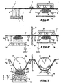
- Figure 1 is a schematic elevational view of a first embodiment, according to the invention, of an installation for the formation of a coating on a substrate.
- Figure 2 is a schematic view, similar to that of the FIG. 1, of a second embodiment, according to the invention, of a installation for the formation of a coating on a substrate.
- Figure 3 is also a schematic view similar to that of FIGS. 1 and 2, of a third embodiment, according to the invention, an installation for the formation of a coating on a substrate.
- Figure 4 is still a schematic view of a fourth embodiment, according to the invention, of an installation for training of a coating on a substrate.
- the invention consists in proposing a process for depositing a coating consisting of a substrate essentially of an electronic conductive compound.
- the substrate can for example be formed from steel sheets at parade, plates of flat glass, sheets of paper or films plastic.
- the coating can be obtained by mass production layers, for example, of metallic or ceramic compounds of which the thickness is generally of the order of 500 to 2000 ⁇ .
- the process according to the invention is characterized by the fact that one first forms a separate layer on the substrate in an element deposition area electronic conductor, such as a metal, alloy, or semiconductor of the N doped type, of a relatively reduced determined thickness. Then, in a reaction zone, which is separate from the deposition zone, a reactive gas containing ions which not only can react with the aforementioned element, but which also have sufficient energy kinetics to be able to be implanted on all the aforementioned determined thickness deposit or layer of the element on the substrate.
- an element deposition area electronic conductor such as a metal, alloy, or semiconductor of the N doped type
- This kinetic energy is advantageously maintained in below 2000 V, preferably between 200 and 900 V, while the aforementioned determined thickness is such that the implantation of the ions of the gas reagent can take place over substantially this entire thickness and that these ions can react with the entire element forming this layer of deposit.
- a plasma into which the aforementioned reactive gas is introduced so as to form there ions which can react, by implantation, with the deposited element previously on the substrate.
- the deposit of the aforementioned conductive element can be formed by evaporation, preferably under vacuum, followed by condensation on the substrate, by sputtering, by a combination of a evaporation and sputtering or by means of a ion gun.
- Figure 1 schematically shows an embodiment in which the deposit of the element is formed by vacuum evaporation. It is a particular embodiment for covering one of the faces of a substrate 1 in the form of a continuous sheet, which moves in a substantially continuous manner in the direction of the arrow 2, d 'first through a first zone 3 where the evaporation takes place under vacuum of a metal 4 kept in fusion in a crucible 5. In this zone, a film or a layer 6 of this metal is condensed on the face of the face facing the crucible 5. The substrate 1 with this film 6 then moves to a second zone 7, separated from the first, in which a plasma 8 is produced, in a reactive gas for example N 2 , CH 4 makes it possible to form ions in this gas. These ions are implanted in the film 6 to react with the metal of which it is made, and thus form a coating 9 of an electronic conductive compound obtained by the reaction of the metal forming the film with the ions produced.
- a reactive gas for example N 2 , CH 4 makes it
- the kinetic energy necessary for penetrate the entire thickness of the film 6 apply to the substrate 1, in the zone 7, a negative potential with respect to an anode 10 arranged opposite of this substrate.
- the reactive gas is introduced into the plasma 8 by injectors 11 shown schematically in FIG. 1 and generally called “showers”.
- the density of the ions entering the film 6 is further increased by the presence of a magnetic confinement circuit on the side of the substrate covered by this film.
- This magnetic circuit is created by magnets permanent or possibly electromagnets 12 mounted on a mild steel plate, shown schematically in Figure 1, arranged at proximity of the substrate 1, on the side opposite to that on which the film 6 is formed.
- Figure 2 is a schematic representation of a second embodiment of the invention which relates to training a coating on one of the faces of rigid plates, in particular of glass 1 moving substantially continuously, in the direction of the arrow 2, on driven rollers 13, earthed, successively through the deposition zone 3 and the reaction zone 7.
- the deposition of the film 6 in the deposition zone 3 is formed by sputtering.
- this technique which is known per se, provision is made in this zone 3, opposite the glass plates 1, a target of magnetron sputtering 14 provided, on the side directed towards these glass plates, a layer of the metal of which the film 6 is made.
- This target layer 14 is bombarded with inert gas ions, such as argon ions, formed in a plasma 15, which eject atoms of metal of this target 14 and form the aforementioned film on the substrate 6.
- This gas inert is introduced into deposition zone 3 by inclined injectors down.
- Target 14 is set to a negative potential, while the rollers 13 are also grounded.
- Reaction zone 7 where the implantation of this ion film takes place from the reactive gas, is substantially identical to that of FIG. 1 and is separated from the deposition zone by a wall 20 in which is arranged an opening 21 for the passage of the glass plates 1 from the zone of deposit 3 to reaction zone 7.
- Figure 3 is a schematic representation of a third embodiment which differs from that shown in Figure 2 by the nature of the substrate 1, of the technique applied for the formation of the metal film 6 in the depot area and means of transport of the substrate 1 through deposition zones 3 and 7.
- the substrate is formed of a flexible sheet 1, of a metal, or of a flexible sheet of paper or plastic, such as polyethylene or polypropylene, which is driven by drums 16 rotating in synchronism around their axis 17 in the direction of the arrows 2.
- the film 6 is formed on the substrate 1 by applying the combined technique of vacuum evaporation and sputtering, as described in the Belgian patent application 09501052 of December 20, 1996 from the same applicant.
- the metal 4 is kept in the state liquid in a crucible 5 maintained at a negative potential, below which are arranged magnets 12 forming a magnetic circuit exactly as in reaction zone 7 of the embodiments previous.
- reaction zone 7 which follows the deposition zone 3 is separated of the latter by a wall 20, as in the second form of production.
- This reaction zone 7 differs from the embodiments previous by the fact that the sheet 1 forming the substrate is driven on a drum 16 and that the magnets 12, forming the magnetic circuit, are arranged inside the drum, opposite the place where the sheet 1 is in contact with the latter.
- One of the advantages of the installation according to FIG. 3 is that it allows easy cooling of the substrate both in the area deposition only in the reaction zone by means of a coolant flowing inside the drums. This can be useful in some cases, for example for the treatment of substrates with relatively softening point low or subject to phase transformations.
- Figure 4 is a schematic representation of a fourth embodiment of the invention in which the formation of film 6 on the substrate 1 in the deposition areas 3 can be produced by example as in the previous embodiments.
- a specific drop zone is separate from the drop zone subsequent deposition by at least two separate consecutive reaction zones.
- two deposition zones 3 are shown, three consecutive reaction zones 7a, 7b, 7c where the substrate 1 is subjected to a potential that differs from a reaction zone to the reaction zone subsequent, preferably at a decreasing potential, in the direction of displacement 2 of the substrate 1, from a reaction zone to the reaction zone next.
- the potential difference in area 7a can by example being of the order of 3000 V, that in zone 7b of 1000 V and that in zone 7c of 500 V.
- This example concerns the formation of a coating of decoration of zirconium nitride on a steel sheet making use of it of an installation as illustrated in FIG. 1 in which however a zirconium film 6 is deposited on the sheet 1, from a zirconium target 14, by sputtering, as in the installation shown in the figure 2.
- the 0.2 mm thick sheet moved through the zones 3 and 7 at a speed of the order of 400 m / minute.
- the width of the target of zirconium 14 in reaction zones 3, in the direction of movement 2 of sheet 1, was 30 cm.
- the passage time of the sheet 1 ahead of target 14 was 0.045 sec.
- argon was injected at a pressure of 0.667 Pa (5.10 -3 Torr), while the power density dissipated at the target was 75 W / cm 2 .
- reaction zone 7 also called implantation zone
- nitrogen was also injected at a pressure of 0.667 Pa (5.10 -3 Torr), while the power density dissipated on the substrate during the implantation of the zirconium film was 20 W / cm 3 .
- the voltage between the sheet and the anode was 450 V.
- This example concerns the formation of an oxide layer indium and tin (InSnO), also called "ITO", on plates glass, making use of the installation as illustrated schematically by Figure 2 but, but in which, however, the deposit area 3 corresponded to that of the embodiment shown in FIG. 1.
- ITO oxide layer indium and tin
- the surface liquid metal in each of these crucibles, exposed to the plates of scrolling glass next to these, was 30 cm wide in the direction of travel As in the first example, the speed of displacement of the plates was 400 m / minute.
- argon was injected at a pressure of 0.667 Pa (5.10 -3 Torr), while the power density dissipated at the targets was 50 W / cm 2 .
- Example 2 As in Example 1, these plates were passed through glass through ten identical deposition zones between each of which was the same reaction zone. This made it possible to obtain plaques of glass covered with a homogeneous and transparent final layer of oxide indium and tin with a thickness of 1000 ⁇ .
- This example concerns the formation of a nitride coating of titanium on a flexible sheet of aluminum with a thickness of 0.3 mm in using an installation of the type shown in Figure 3.
- the working conditions and parameters in the areas of deposition and reaction corresponded substantially to those of Example 1. This made it possible to obtain a homogeneous coating of titanium nitride of a thickness of 500 ⁇ after ten successive passes through an area of depot and a reaction zone.
Landscapes
- Chemical & Material Sciences (AREA)
- Chemical Kinetics & Catalysis (AREA)
- Engineering & Computer Science (AREA)
- Materials Engineering (AREA)
- Mechanical Engineering (AREA)
- Metallurgy (AREA)
- Organic Chemistry (AREA)
- Physical Vapour Deposition (AREA)
- Non-Metallic Protective Coatings For Printed Circuits (AREA)
- Chemical Vapour Deposition (AREA)
Description
Claims (17)
- Procédé pour le dépôt sur un substrat (1) d'un revêtement (6) comprenant un composé conducteur électronique suivant lequel on forme le revêtement, en produisant, d'une part, dans au moins une zone de dépôt (3), un ou plusieurs dépôts d'une épaisseur déterminée d'un élément conducteur électronique; et en produisant, d'autre part, dans au moins une zone de réaction (7) dans laquelle est située une anode (10), une ou plusieurs réactions de l'élément conducteur électronique ainsi déposé avec des ions d'un gaz réactif afin de les implanter dans le dépôt de l'élément susdit sur la majorité de cette épaisseur déterminée de manière à former avec la majorité de cet élément ledit composé conducteur électronique;
dans lequel un potentiel négatif par rapport à l'anode (10) est appliqué dans la zone de réaction (7) au revêtement déposé (6). - Procédé suivant la revendication 1, dans lequel le potentiel négatif est appliqué au revêtement déposé en appliquant au substrat un potentiel négatif par rapport à l'anode.
- Procédé suivant la revendication 1, dans lequel le potentiel négatif est appliqué au revêtement déposé en mettant des rouleaux (13), qui sont en contact avec le revêtement, à la masse.
- Procédé suivant l'une quelconque des revendications 1 à 3, dans lequel les ions sont soumis à une différence de potentiel inférieure à 2000 V, de préférence de 200 à 900 V.
- Procédé suivant l'une quelconque des revendications 1 à 4, dans lequel l'on effectue la réaction précitée de l'élément déposé sur le substrat avec le gaz réactif précité en créant, en regard et à proximité de la surface de ce dernier présentant le dépôt de l'élément, un plasma dans lequel on introduit le gaz réactif précité, de manière à y former ainsi des ions pénétrant dans le dépôt de l'élément, sensiblement sur une profondeur correspondant à l'épaisseur de ce dépôt, pour les faire réagir avec l'élément.
- Procédé suivant rune quelconque des revendications 1 à 5, dans lequel l'on forme le dépôt de l'élément sur le substrat par évaporation, de préférence sous vide, suivie d'une condensation.
- Procédé suivant l'une quelconque des revendications 1 à 6, dans lequel l'on forme le dépôt de l'élément sur le substrat par pulvérisation cathodique.
- Procédé suivant l'une quelconque des revendications 5 à 7, dans lequel l'on forme sur le substrat un revêtement constitué d'une couche d'un composé céramique conducteur électronique, par exemple un composé du type TiN, ZrN, TiCN, CrN, VN, NbN, obtenu par la réaction d'un métal et d'un gaz réactif, en effectuant d'abord, dans la zone de dépôt, un dépôt dudit métal sur le substrat et, ensuite, dans la zone de réaction, une ionisation du gaz dans un plasma, formé en regard de ce dépôt, et une implantation de particules ionisées de ce gaz dans ce dépôt de métal, ce dernier étant mis à un potentiel négatif par rapport au gaz ionisé.
- Procédé suivant l'une quelconque des revendications 1 à 8, dans lequel l'on crée un circuit magnétique de confinement des électrons du côté du substrat où a lieu la réaction de l'élément déposé avec le gaz réactif précité.
- Procédé suivant l'une quelconque des revendications 1 à 9, dans lequel l'on prévoit, après chaque zone de dépôt de l'élément précité, au moins deux zones de réaction successives séparées, le substrat étant soumis à un potentiel différent d'une zone de réaction à la zone de réaction subséquente.
- Procédé suivant l'une quelconque des revendications 1 à 10, dans lequel le substrat est formé dune bande continue se déplaçant, de préférence d'une manière sensiblement continue, à travers les zones successives précitées.
- Procédé suivant l'une quelconque des revendications 1 à 11, dans lequel le substrat étant formé d'une plaque, de telles plaques successives sont déplacées l'une à la suite de l'autre à travers les zones successives, le dépôt formé sur ces plaques dans la zone de dépôt étant mis à un potentiel négatif au moins dans la zone de réaction.
- Procédé suivant l'une quelconque des revendications 1 à 12, dans lequel une excitation radio-fréquence, de préférence dans la gamme des micro-ondes, est appliquée dans la zone de réaction précitée, à proximité de la surface du substrat sur laquelle l'on forme le revêtement.
- Installation pour le dépôt, sur un substrat, d'un revêtement constitué essentiellement d'un composé conducteur électronique, notamment installation pour la mise en oeuvre du procédé suivant l'une quelconque des revendications 1 à 13, comprenant au moins une zone de dépôt, dans laquelle peut se former un dépôt d'un élément conducteur électronique sur le substrat, cette zone de dépôt étant suivie d'au moins une zone de réaction séparée de cette zone de dépôt, où peut être créée une implantation, dans le dépôt susdit, de particules pouvant réagir avec cet élément pour former le composé conducteur électronique, des moyens étant prévus pour déplacer le substrat de la zone de dépôt vers la zone de réaction, caractérisée en ce que des moyens sont prévus pour appliquer au revêtement, au moins dans la zone de réaction, un potentiel négatif par rapport à une anode agencée dans cette zone en regard du substrat.
- Installation suivant la revendication 14, dans laquelle la zone de dépôt précitée comprend un dispositif permettant de créer une évaporation, de préférence sous vide, suivie d'une condensation de l'élément sur le substrat.
- Installation suivant la revendication 14, dans laquelle la zone de dépôt comprend une cible présentant une couche superficielle orientée vers le substrat et contenant l'élément à déposer sur ce dernier, des moyens étant prévus pour former un dépôt de cet élément à partir de cette cible par pulvérisation cathodique.
- Installation suivant l'une quelconque des revendications 14 à 16, comprenant dans la zone de réaction, des moyens permettant d'ioniser des particules de gaz pouvant s'implanter dans le dépôt de l'élément conducteur électronique précité.
Applications Claiming Priority (2)
| Application Number | Priority Date | Filing Date | Title |
|---|---|---|---|
| BE9600637 | 1996-07-12 | ||
| BE9600637A BE1010420A3 (fr) | 1996-07-12 | 1996-07-12 | Procede pour la formation d'un revetement sur un substrat et installation pour la mise en oeuvre de ce procede. |
Publications (2)
| Publication Number | Publication Date |
|---|---|
| EP0818557A1 EP0818557A1 (fr) | 1998-01-14 |
| EP0818557B1 true EP0818557B1 (fr) | 2001-08-29 |
Family
ID=3889877
Family Applications (1)
| Application Number | Title | Priority Date | Filing Date |
|---|---|---|---|
| EP97870100A Expired - Lifetime EP0818557B1 (fr) | 1996-07-12 | 1997-07-08 | Procédé et installation pour la formation d'un revêtement sur un substrat |
Country Status (8)
| Country | Link |
|---|---|
| US (2) | US6171659B1 (fr) |
| EP (1) | EP0818557B1 (fr) |
| AT (1) | ATE204927T1 (fr) |
| BE (1) | BE1010420A3 (fr) |
| DE (1) | DE69706380T2 (fr) |
| DK (1) | DK0818557T3 (fr) |
| ES (1) | ES2162670T3 (fr) |
| PT (1) | PT818557E (fr) |
Families Citing this family (21)
| Publication number | Priority date | Publication date | Assignee | Title |
|---|---|---|---|---|
| US6964731B1 (en) * | 1998-12-21 | 2005-11-15 | Cardinal Cg Company | Soil-resistant coating for glass surfaces |
| US6676810B2 (en) * | 2000-01-12 | 2004-01-13 | D2 In-Line Solutions, Llc | Method of coating insulative substrates |
| AUPR515301A0 (en) * | 2001-05-22 | 2001-06-14 | Commonwealth Scientific And Industrial Research Organisation | Process and apparatus for producing crystalline thin film buffer layers and structures having biaxial texture |
| AU2002302168B2 (en) * | 2001-05-22 | 2007-11-08 | Commonwealth Scientific And Industrial Research Organisation | Process and apparatus for producing crystalline thin film buffer layers and structures having biaxial texture |
| EP1490527A1 (fr) * | 2002-03-29 | 2004-12-29 | D2 In-Line Solutions, LLC | Systeme et procede de traitement continu en ligne a alimentation par gravite |
| EP1579027B1 (fr) * | 2002-12-18 | 2006-04-19 | Cardinal CG Company | Depot de couches active par plasma |
| EP1579025B1 (fr) * | 2002-12-31 | 2010-09-29 | Cardinal CG Company | Machine a enduire comportant un dispositif de nettoyage de substrat et procede de depot de revetement mettant en oeuvre une telle machine |
| US7128133B2 (en) * | 2003-12-16 | 2006-10-31 | 3M Innovative Properties Company | Hydrofluoroether as a heat-transfer fluid |
| US7294404B2 (en) * | 2003-12-22 | 2007-11-13 | Cardinal Cg Company | Graded photocatalytic coatings |
| ATE377580T1 (de) * | 2004-07-12 | 2007-11-15 | Cardinal Cg Co | Wartungsarme beschichtungen |
| WO2006080968A2 (fr) * | 2004-11-15 | 2006-08-03 | Cardinal Cg Company | Procedes et equipement pour deposer des revetements presentant des structures ordonnees |
| US8092660B2 (en) * | 2004-12-03 | 2012-01-10 | Cardinal Cg Company | Methods and equipment for depositing hydrophilic coatings, and deposition technologies for thin films |
| US7923114B2 (en) * | 2004-12-03 | 2011-04-12 | Cardinal Cg Company | Hydrophilic coatings, methods for depositing hydrophilic coatings, and improved deposition technology for thin films |
| JP2009534563A (ja) | 2006-04-19 | 2009-09-24 | 日本板硝子株式会社 | 同等の単独の表面反射率を有する対向機能コーティング |
| US20080011599A1 (en) | 2006-07-12 | 2008-01-17 | Brabender Dennis M | Sputtering apparatus including novel target mounting and/or control |
| JP5452928B2 (ja) * | 2006-09-27 | 2014-03-26 | ダブリュディ・メディア・シンガポール・プライベートリミテッド | 磁気記録媒体の製造方法、及び積層体の製造方法 |
| CA2664369A1 (fr) | 2007-09-14 | 2009-03-19 | Cardinal Cg Company | Revetements a faible entretien et procedes de production de revetements a faible entretien |
| BE1017852A3 (fr) * | 2007-11-19 | 2009-09-01 | Ind Plasma Services & Technologies Ipst Gmbh | Procede et installation de galvanisation par evaporation plasma. |
| DE102013110328B4 (de) * | 2013-09-19 | 2018-05-09 | VON ARDENNE Asset GmbH & Co. KG | Beschichtungsanordnung und Beschichtungsverfahren |
| US10604442B2 (en) | 2016-11-17 | 2020-03-31 | Cardinal Cg Company | Static-dissipative coating technology |
| CN118028762B (zh) * | 2024-04-12 | 2024-07-09 | 山东省宝丰镀膜有限公司 | 一种悬浮式卷绕磁控阴极轰击蒸发成膜系统 |
Family Cites Families (14)
| Publication number | Priority date | Publication date | Assignee | Title |
|---|---|---|---|---|
| US3594238A (en) * | 1968-08-15 | 1971-07-20 | United States Steel Corp | Method for treating aluminum surfaces to prevent discoloration |
| JPS56163262A (en) * | 1980-05-21 | 1981-12-15 | Ulvac Corp | Method and apparatus for forming oxidation and weather resistant film after surface treatment |
| US4478703A (en) * | 1983-03-31 | 1984-10-23 | Kawasaki Jukogyo Kabushiki Kaisha | Sputtering system |
| JPS60141869A (ja) * | 1983-12-29 | 1985-07-26 | Nissin Electric Co Ltd | 膜形成方法および膜形成装置 |
| GB8423255D0 (en) * | 1984-09-14 | 1984-10-17 | Atomic Energy Authority Uk | Surface treatment of metals |
| US4708037A (en) * | 1985-11-18 | 1987-11-24 | Gte Laboratories Incorporated | Coated cemented carbide tool for steel roughing applications and methods for machining |
| GB8626330D0 (en) * | 1986-11-04 | 1986-12-31 | Atomic Energy Authority Uk | Ion assisted coatings |
| DE3641718A1 (de) * | 1986-12-06 | 1988-06-16 | Leybold Ag | Verfahren zum herstellen von wickeln aus im vakuum leitfaehig beschichteten isolierstoff-folien |
| JPS63206464A (ja) * | 1987-02-23 | 1988-08-25 | Asahi Glass Co Ltd | インライン型複合表面処理装置 |
| US4851095A (en) * | 1988-02-08 | 1989-07-25 | Optical Coating Laboratory, Inc. | Magnetron sputtering apparatus and process |
| JPH01294861A (ja) * | 1988-05-20 | 1989-11-28 | Hitachi Koki Co Ltd | イオンビームミキシング法 |
| US5241152A (en) * | 1990-03-23 | 1993-08-31 | Anderson Glen L | Circuit for detecting and diverting an electrical arc in a glow discharge apparatus |
| US5346600A (en) * | 1992-08-14 | 1994-09-13 | Hughes Aircraft Company | Plasma-enhanced magnetron-sputtered deposition of materials |
| JP3291088B2 (ja) * | 1993-10-06 | 2002-06-10 | 株式会社神戸製鋼所 | 被膜形成方法 |
-
1996
- 1996-07-12 BE BE9600637A patent/BE1010420A3/fr not_active IP Right Cessation
-
1997
- 1997-07-08 DK DK97870100T patent/DK0818557T3/da active
- 1997-07-08 AT AT97870100T patent/ATE204927T1/de active
- 1997-07-08 ES ES97870100T patent/ES2162670T3/es not_active Expired - Lifetime
- 1997-07-08 DE DE69706380T patent/DE69706380T2/de not_active Expired - Lifetime
- 1997-07-08 EP EP97870100A patent/EP0818557B1/fr not_active Expired - Lifetime
- 1997-07-08 PT PT97870100T patent/PT818557E/pt unknown
- 1997-07-11 US US08/893,578 patent/US6171659B1/en not_active Expired - Lifetime
-
2001
- 2001-01-05 US US09/754,401 patent/US6337005B2/en not_active Expired - Lifetime
Non-Patent Citations (2)
| Title |
|---|
| Advanced techniques for surface engineering, W. Gissler and H. A. Jehn, Kluwer Academic Publishers * |
| Handbook of deposition technologies for films and coatings, Rointan F. Bunshah, Noyes publications * |
Also Published As
| Publication number | Publication date |
|---|---|
| US6337005B2 (en) | 2002-01-08 |
| DK0818557T3 (da) | 2002-01-07 |
| DE69706380T2 (de) | 2002-05-08 |
| ES2162670T3 (es) | 2002-01-01 |
| PT818557E (pt) | 2002-02-28 |
| EP0818557A1 (fr) | 1998-01-14 |
| US20010001948A1 (en) | 2001-05-31 |
| ATE204927T1 (de) | 2001-09-15 |
| BE1010420A3 (fr) | 1998-07-07 |
| US6171659B1 (en) | 2001-01-09 |
| DE69706380D1 (de) | 2001-10-04 |
Similar Documents
| Publication | Publication Date | Title |
|---|---|---|
| BE1010420A3 (fr) | Procede pour la formation d'un revetement sur un substrat et installation pour la mise en oeuvre de ce procede. | |
| EP0038294B1 (fr) | Procédé de dépôt d'un revêtement dur métallique, cible de dépôt pour un tel procédé et pièce de joaillerie comportant un tel revêtement | |
| CA1093910A (fr) | Depot reactif d'oxydes | |
| FR2500852A1 (fr) | ||
| EP1182272A1 (fr) | Procédé et dispositif permettant le dépôt de couches métalliques en continu par plasma froid | |
| FR2578270A1 (fr) | Procede de vaporisation reactive de couches d'oxyde, de nitrure, d'oxynitrure et de carbure. | |
| KR970003431A (ko) | 개선된 질화 티타늄 함유 방지층을 형성하기 위한 연속적인 방법 | |
| US20030186493A1 (en) | Method and device for making substrates | |
| FR2957454A1 (fr) | Procede de conditionnement d'un canon a ions | |
| WO1996012389A9 (fr) | Appareil destine a deposer une couche de matiere sur un substrat | |
| WO1996012389A1 (fr) | Appareil destine a deposer une couche de matiere sur un substrat | |
| EP0413617A1 (fr) | ProcÀ©dé de dépôt de couches minces | |
| FR2596775A1 (fr) | Revetement dur multicouches elabore par depot ionique de nitrure de titane, carbonitrure de titane et i-carbone | |
| RU97112300A (ru) | Способ формирования износостойкого покрытия на поверхности изделий из конструкционной стали | |
| EP2111477B1 (fr) | Procédé de revêtement d'un substrat, installation de mise en oeuvre du procédé et dispositif d'alimentation en métal d'une telle installation | |
| FR2559507A1 (fr) | Procede de fabrication de materiau stratifie ou de pieces stratifiees | |
| FR2843130A1 (fr) | Procede de revetement de la surface d'un materiau metallique, dispositif pour sa mise en oeuvre et produit ainsi obtenu | |
| CH627791A5 (en) | Process for covering the surface of an electrically conductive article, plant for making use of the process and application of the process | |
| AU2002364794A1 (en) | Improved method for coating a support | |
| EP0908924A1 (fr) | Dispositif pour la formation d'un revêtement sur un substrat par condensation | |
| EP0365386A1 (fr) | Procédé pour rendre une glace en matière plastique résistante à l'ábrasion et glace en matière plastique rendue résistante à l'ábrasion | |
| CH665488A5 (fr) | Procede pour realiser un composant optique et composant obtenu par ce procede. | |
| EP4213181B1 (fr) | Procédé d'activation d'une couche exposée | |
| FR2528452A1 (fr) | Procede et dispositif pour la realisation de depots metalliques ou de composes metalliques, a la surface d'une piece en un materiau electriquement conducteur | |
| FR2541690A1 (fr) | Dispositif et procede de revetement de substrats par decharge luminescente et emploi de ceux-ci |
Legal Events
| Date | Code | Title | Description |
|---|---|---|---|
| PUAI | Public reference made under article 153(3) epc to a published international application that has entered the european phase |
Free format text: ORIGINAL CODE: 0009012 |
|
| AK | Designated contracting states |
Kind code of ref document: A1 Designated state(s): AT BE CH DE DK ES FI FR GB GR IE IT LI LU NL PT SE |
|
| AX | Request for extension of the european patent |
Free format text: AL;LT;LV;RO;SI |
|
| 17P | Request for examination filed |
Effective date: 19980330 |
|
| AKX | Designation fees paid |
Free format text: AT BE CH DE DK ES FI FR GB GR IE IT LI LU NL PT SE |
|
| RBV | Designated contracting states (corrected) |
Designated state(s): AT BE CH DE DK ES FI FR GB GR IE IT LI LU NL PT SE |
|
| 17Q | First examination report despatched |
Effective date: 19981230 |
|
| GRAG | Despatch of communication of intention to grant |
Free format text: ORIGINAL CODE: EPIDOS AGRA |
|
| GRAG | Despatch of communication of intention to grant |
Free format text: ORIGINAL CODE: EPIDOS AGRA |
|
| GRAH | Despatch of communication of intention to grant a patent |
Free format text: ORIGINAL CODE: EPIDOS IGRA |
|
| GRAH | Despatch of communication of intention to grant a patent |
Free format text: ORIGINAL CODE: EPIDOS IGRA |
|
| GRAA | (expected) grant |
Free format text: ORIGINAL CODE: 0009210 |
|
| AK | Designated contracting states |
Kind code of ref document: B1 Designated state(s): AT BE CH DE DK ES FI FR GB GR IE IT LI LU NL PT SE |
|
| REF | Corresponds to: |
Ref document number: 204927 Country of ref document: AT Date of ref document: 20010915 Kind code of ref document: T |
|
| REG | Reference to a national code |
Ref country code: CH Ref legal event code: EP |
|
| REG | Reference to a national code |
Ref country code: IE Ref legal event code: FG4D Free format text: FRENCH |
|
| REF | Corresponds to: |
Ref document number: 69706380 Country of ref document: DE Date of ref document: 20011004 |
|
| REG | Reference to a national code |
Ref country code: CH Ref legal event code: NV Representative=s name: E. BLUM & CO. PATENTANWAELTE |
|
| REG | Reference to a national code |
Ref country code: GB Ref legal event code: IF02 Ref country code: ES Ref legal event code: FG2A Ref document number: 2162670 Country of ref document: ES Kind code of ref document: T3 |
|
| GBT | Gb: translation of ep patent filed (gb section 77(6)(a)/1977) |
Effective date: 20011130 |
|
| REG | Reference to a national code |
Ref country code: DK Ref legal event code: T3 |
|
| REG | Reference to a national code |
Ref country code: PT Ref legal event code: SC4A Free format text: AVAILABILITY OF NATIONAL TRANSLATION Effective date: 20011108 |
|
| REG | Reference to a national code |
Ref country code: GR Ref legal event code: EP Ref document number: 20010402195 Country of ref document: GR |
|
| PLBE | No opposition filed within time limit |
Free format text: ORIGINAL CODE: 0009261 |
|
| STAA | Information on the status of an ep patent application or granted ep patent |
Free format text: STATUS: NO OPPOSITION FILED WITHIN TIME LIMIT |
|
| 26N | No opposition filed |
Opponent name: AICHELIN GESMBH Effective date: 20020406 |
|
| REG | Reference to a national code |
Ref country code: CH Ref legal event code: PFA Owner name: RECHERCHE ET DEVELOPPEMENT DU GROUPE COCKERILL SA Free format text: RECHERCHE ET DEVELOPPEMENT DU GROUPE COCKERILL SAMBRE, EN ABREGE: RD-CS#CAMPUS UNIVERSITAIRE DU SART TILMAN, BOULEVARD DE COLONSTER B 57#4000 LIEGE (BE) -TRANSFER TO- RECHERCHE ET DEVELOPPEMENT DU GROUPE COCKERILL SAMBRE, EN ABREGE: RD-CS#CAMPUS UNIVERSITAIRE DU SART TILMAN, BOULEVARD DE COLONSTER B 57#4000 LIEGE (BE) |
|
| REG | Reference to a national code |
Ref country code: FR Ref legal event code: PLFP Year of fee payment: 19 |
|
| REG | Reference to a national code |
Ref country code: DE Ref legal event code: R082 Ref document number: 69706380 Country of ref document: DE Representative=s name: HOEGER, STELLRECHT & PARTNER PATENTANWAELTE MB, DE |
|
| REG | Reference to a national code |
Ref country code: FR Ref legal event code: PLFP Year of fee payment: 20 |
|
| PGFP | Annual fee paid to national office [announced via postgrant information from national office to epo] |
Ref country code: CH Payment date: 20160621 Year of fee payment: 20 Ref country code: FI Payment date: 20160622 Year of fee payment: 20 Ref country code: IE Payment date: 20160622 Year of fee payment: 20 Ref country code: ES Payment date: 20160623 Year of fee payment: 20 Ref country code: GR Payment date: 20160622 Year of fee payment: 20 Ref country code: GB Payment date: 20160627 Year of fee payment: 20 |
|
| PGFP | Annual fee paid to national office [announced via postgrant information from national office to epo] |
Ref country code: LU Payment date: 20160713 Year of fee payment: 20 Ref country code: PT Payment date: 20160630 Year of fee payment: 20 Ref country code: FR Payment date: 20160622 Year of fee payment: 20 Ref country code: BE Payment date: 20160621 Year of fee payment: 20 Ref country code: NL Payment date: 20160623 Year of fee payment: 20 Ref country code: DK Payment date: 20160622 Year of fee payment: 20 Ref country code: SE Payment date: 20160627 Year of fee payment: 20 |
|
| PGFP | Annual fee paid to national office [announced via postgrant information from national office to epo] |
Ref country code: IT Payment date: 20160627 Year of fee payment: 20 Ref country code: DE Payment date: 20160622 Year of fee payment: 20 |
|
| PGFP | Annual fee paid to national office [announced via postgrant information from national office to epo] |
Ref country code: AT Payment date: 20160622 Year of fee payment: 20 |
|
| REG | Reference to a national code |
Ref country code: DE Ref legal event code: R071 Ref document number: 69706380 Country of ref document: DE |
|
| REG | Reference to a national code |
Ref country code: NL Ref legal event code: MK Effective date: 20170707 |
|
| REG | Reference to a national code |
Ref country code: CH Ref legal event code: PL |
|
| REG | Reference to a national code |
Ref country code: DK Ref legal event code: EUP Effective date: 20170708 |
|
| REG | Reference to a national code |
Ref country code: GB Ref legal event code: PE20 Expiry date: 20170707 |
|
| REG | Reference to a national code |
Ref country code: AT Ref legal event code: MK07 Ref document number: 204927 Country of ref document: AT Kind code of ref document: T Effective date: 20170708 |
|
| REG | Reference to a national code |
Ref country code: IE Ref legal event code: MK9A |
|
| PG25 | Lapsed in a contracting state [announced via postgrant information from national office to epo] |
Ref country code: PT Free format text: LAPSE BECAUSE OF EXPIRATION OF PROTECTION Effective date: 20170718 Ref country code: IE Free format text: LAPSE BECAUSE OF EXPIRATION OF PROTECTION Effective date: 20170708 Ref country code: GB Free format text: LAPSE BECAUSE OF EXPIRATION OF PROTECTION Effective date: 20170707 |
|
| REG | Reference to a national code |
Ref country code: ES Ref legal event code: FD2A Effective date: 20180508 |
|
| PG25 | Lapsed in a contracting state [announced via postgrant information from national office to epo] |
Ref country code: ES Free format text: LAPSE BECAUSE OF EXPIRATION OF PROTECTION Effective date: 20170709 |