EP0817540A2 - Eletrolumineszierende Anordnungen unter Verwendung von lamellaren Elektroden - Google Patents
Eletrolumineszierende Anordnungen unter Verwendung von lamellaren Elektroden Download PDFInfo
- Publication number
- EP0817540A2 EP0817540A2 EP97110256A EP97110256A EP0817540A2 EP 0817540 A2 EP0817540 A2 EP 0817540A2 EP 97110256 A EP97110256 A EP 97110256A EP 97110256 A EP97110256 A EP 97110256A EP 0817540 A2 EP0817540 A2 EP 0817540A2
- Authority
- EP
- European Patent Office
- Prior art keywords
- layer
- electroluminescent
- lamellar
- electroluminescent element
- anode
- Prior art date
- Legal status (The legal status is an assumption and is not a legal conclusion. Google has not performed a legal analysis and makes no representation as to the accuracy of the status listed.)
- Withdrawn
Links
- 239000000758 substrate Substances 0.000 claims abstract description 8
- 229910010272 inorganic material Inorganic materials 0.000 claims abstract description 4
- 239000011147 inorganic material Substances 0.000 claims abstract description 4
- 239000000463 material Substances 0.000 claims description 13
- 229920000172 poly(styrenesulfonic acid) Polymers 0.000 claims description 4
- 229940005642 polystyrene sulfonic acid Drugs 0.000 claims description 4
- -1 polyethylene Polymers 0.000 claims description 2
- 230000003595 spectral effect Effects 0.000 claims description 2
- 239000004698 Polyethylene Substances 0.000 claims 1
- 229920000573 polyethylene Polymers 0.000 claims 1
- 150000003460 sulfonic acids Chemical class 0.000 claims 1
- 239000004020 conductor Substances 0.000 abstract description 4
- 238000001228 spectrum Methods 0.000 abstract 1
- 239000010410 layer Substances 0.000 description 36
- 238000004519 manufacturing process Methods 0.000 description 8
- 229920000553 poly(phenylenevinylene) Polymers 0.000 description 6
- 238000000034 method Methods 0.000 description 5
- 239000000243 solution Substances 0.000 description 5
- IJGRMHOSHXDMSA-UHFFFAOYSA-N Atomic nitrogen Chemical compound N#N IJGRMHOSHXDMSA-UHFFFAOYSA-N 0.000 description 4
- 229920001609 Poly(3,4-ethylenedioxythiophene) Polymers 0.000 description 4
- 229910052751 metal Inorganic materials 0.000 description 4
- 239000002184 metal Substances 0.000 description 4
- 239000000203 mixture Substances 0.000 description 4
- 229920000642 polymer Polymers 0.000 description 4
- XOLBLPGZBRYERU-UHFFFAOYSA-N tin dioxide Chemical compound O=[Sn]=O XOLBLPGZBRYERU-UHFFFAOYSA-N 0.000 description 4
- 229910001887 tin oxide Inorganic materials 0.000 description 4
- 229910045601 alloy Inorganic materials 0.000 description 3
- 239000000956 alloy Substances 0.000 description 3
- 238000005266 casting Methods 0.000 description 3
- 239000011248 coating agent Substances 0.000 description 3
- 238000000576 coating method Methods 0.000 description 3
- 230000005684 electric field Effects 0.000 description 3
- 239000012044 organic layer Substances 0.000 description 3
- RPACBEVZENYWOL-XFULWGLBSA-M sodium;(2r)-2-[6-(4-chlorophenoxy)hexyl]oxirane-2-carboxylate Chemical compound [Na+].C=1C=C(Cl)C=CC=1OCCCCCC[C@]1(C(=O)[O-])CO1 RPACBEVZENYWOL-XFULWGLBSA-M 0.000 description 3
- SCYULBFZEHDVBN-UHFFFAOYSA-N 1,1-Dichloroethane Chemical compound CC(Cl)Cl SCYULBFZEHDVBN-UHFFFAOYSA-N 0.000 description 2
- 229920000144 PEDOT:PSS Polymers 0.000 description 2
- XLOMVQKBTHCTTD-UHFFFAOYSA-N Zinc monoxide Chemical compound [Zn]=O XLOMVQKBTHCTTD-UHFFFAOYSA-N 0.000 description 2
- HSFWRNGVRCDJHI-UHFFFAOYSA-N alpha-acetylene Natural products C#C HSFWRNGVRCDJHI-UHFFFAOYSA-N 0.000 description 2
- 239000011521 glass Substances 0.000 description 2
- 229910052737 gold Inorganic materials 0.000 description 2
- 239000010931 gold Substances 0.000 description 2
- 238000010438 heat treatment Methods 0.000 description 2
- AMGQUBHHOARCQH-UHFFFAOYSA-N indium;oxotin Chemical compound [In].[Sn]=O AMGQUBHHOARCQH-UHFFFAOYSA-N 0.000 description 2
- 238000002347 injection Methods 0.000 description 2
- 239000007924 injection Substances 0.000 description 2
- 229910044991 metal oxide Inorganic materials 0.000 description 2
- 150000004706 metal oxides Chemical class 0.000 description 2
- 229910052757 nitrogen Inorganic materials 0.000 description 2
- 229920001197 polyacetylene Polymers 0.000 description 2
- 229920002959 polymer blend Polymers 0.000 description 2
- 229920000123 polythiophene Polymers 0.000 description 2
- 239000004065 semiconductor Substances 0.000 description 2
- 238000004544 sputter deposition Methods 0.000 description 2
- 239000012780 transparent material Substances 0.000 description 2
- JBRZTFJDHDCESZ-UHFFFAOYSA-N AsGa Chemical compound [As]#[Ga] JBRZTFJDHDCESZ-UHFFFAOYSA-N 0.000 description 1
- 229910001218 Gallium arsenide Inorganic materials 0.000 description 1
- 229910052782 aluminium Inorganic materials 0.000 description 1
- 239000002800 charge carrier Substances 0.000 description 1
- 238000005234 chemical deposition Methods 0.000 description 1
- 239000003795 chemical substances by application Substances 0.000 description 1
- 229910052804 chromium Inorganic materials 0.000 description 1
- 150000001875 compounds Chemical class 0.000 description 1
- 229920001940 conductive polymer Polymers 0.000 description 1
- 238000010276 construction Methods 0.000 description 1
- 229910052802 copper Inorganic materials 0.000 description 1
- 238000000151 deposition Methods 0.000 description 1
- 230000008021 deposition Effects 0.000 description 1
- 238000005401 electroluminescence Methods 0.000 description 1
- 238000005538 encapsulation Methods 0.000 description 1
- 239000005357 flat glass Substances 0.000 description 1
- 229920005570 flexible polymer Polymers 0.000 description 1
- 239000007789 gas Substances 0.000 description 1
- PCHJSUWPFVWCPO-UHFFFAOYSA-N gold Chemical compound [Au] PCHJSUWPFVWCPO-UHFFFAOYSA-N 0.000 description 1
- 238000005259 measurement Methods 0.000 description 1
- 150000002739 metals Chemical class 0.000 description 1
- 229910052759 nickel Inorganic materials 0.000 description 1
- 230000003287 optical effect Effects 0.000 description 1
- 150000002894 organic compounds Chemical class 0.000 description 1
- 229920000767 polyaniline Polymers 0.000 description 1
- 229920000128 polypyrrole Polymers 0.000 description 1
- 239000000523 sample Substances 0.000 description 1
- 229910052709 silver Inorganic materials 0.000 description 1
- 238000004528 spin coating Methods 0.000 description 1
- 239000000126 substance Substances 0.000 description 1
- 230000003746 surface roughness Effects 0.000 description 1
- 238000010345 tape casting Methods 0.000 description 1
- 238000007740 vapor deposition Methods 0.000 description 1
- 238000005019 vapor deposition process Methods 0.000 description 1
- 208000008918 voyeurism Diseases 0.000 description 1
- 238000007704 wet chemistry method Methods 0.000 description 1
- 239000011787 zinc oxide Substances 0.000 description 1
Classifications
-
- H—ELECTRICITY
- H05—ELECTRIC TECHNIQUES NOT OTHERWISE PROVIDED FOR
- H05B—ELECTRIC HEATING; ELECTRIC LIGHT SOURCES NOT OTHERWISE PROVIDED FOR; CIRCUIT ARRANGEMENTS FOR ELECTRIC LIGHT SOURCES, IN GENERAL
- H05B33/00—Electroluminescent light sources
- H05B33/12—Light sources with substantially two-dimensional radiating surfaces
- H05B33/26—Light sources with substantially two-dimensional radiating surfaces characterised by the composition or arrangement of the conductive material used as an electrode
-
- H—ELECTRICITY
- H10—SEMICONDUCTOR DEVICES; ELECTRIC SOLID-STATE DEVICES NOT OTHERWISE PROVIDED FOR
- H10K—ORGANIC ELECTRIC SOLID-STATE DEVICES
- H10K50/00—Organic light-emitting devices
- H10K50/80—Constructional details
- H10K50/805—Electrodes
- H10K50/81—Anodes
- H10K50/816—Multilayers, e.g. transparent multilayers
-
- H—ELECTRICITY
- H10—SEMICONDUCTOR DEVICES; ELECTRIC SOLID-STATE DEVICES NOT OTHERWISE PROVIDED FOR
- H10K—ORGANIC ELECTRIC SOLID-STATE DEVICES
- H10K50/00—Organic light-emitting devices
- H10K50/10—OLEDs or polymer light-emitting diodes [PLED]
- H10K50/17—Carrier injection layers
-
- H—ELECTRICITY
- H10—SEMICONDUCTOR DEVICES; ELECTRIC SOLID-STATE DEVICES NOT OTHERWISE PROVIDED FOR
- H10K—ORGANIC ELECTRIC SOLID-STATE DEVICES
- H10K85/00—Organic materials used in the body or electrodes of devices covered by this subclass
- H10K85/10—Organic polymers or oligomers
- H10K85/111—Organic polymers or oligomers comprising aromatic, heteroaromatic, or aryl chains, e.g. polyaniline, polyphenylene or polyphenylene vinylene
- H10K85/113—Heteroaromatic compounds comprising sulfur or selene, e.g. polythiophene
- H10K85/1135—Polyethylene dioxythiophene [PEDOT]; Derivatives thereof
-
- H—ELECTRICITY
- H10—SEMICONDUCTOR DEVICES; ELECTRIC SOLID-STATE DEVICES NOT OTHERWISE PROVIDED FOR
- H10K—ORGANIC ELECTRIC SOLID-STATE DEVICES
- H10K85/00—Organic materials used in the body or electrodes of devices covered by this subclass
- H10K85/60—Organic compounds having low molecular weight
- H10K85/631—Amine compounds having at least two aryl rest on at least one amine-nitrogen atom, e.g. triphenylamine
- H10K85/633—Amine compounds having at least two aryl rest on at least one amine-nitrogen atom, e.g. triphenylamine comprising polycyclic condensed aromatic hydrocarbons as substituents on the nitrogen atom
-
- H—ELECTRICITY
- H10—SEMICONDUCTOR DEVICES; ELECTRIC SOLID-STATE DEVICES NOT OTHERWISE PROVIDED FOR
- H10K—ORGANIC ELECTRIC SOLID-STATE DEVICES
- H10K85/00—Organic materials used in the body or electrodes of devices covered by this subclass
- H10K85/60—Organic compounds having low molecular weight
- H10K85/649—Aromatic compounds comprising a hetero atom
- H10K85/657—Polycyclic condensed heteroaromatic hydrocarbons
- H10K85/6572—Polycyclic condensed heteroaromatic hydrocarbons comprising only nitrogen in the heteroaromatic polycondensed ring system, e.g. phenanthroline or carbazole
Definitions
- An electroluminescent (EL) arrangement is characterized in that it emits light under the application of an electrical voltage under current flow.
- polymers such as poly- (p-phenylene) and poly- (p-phenylene vinylene (PPV)) as electroluminescent polymers: G. Leising et al., Adv. Mater. 4 (1992) No. 1; Friend et al., J. Chem. Soc., Chem. Commun. 32 (1992); Saito et al., Polymer, 1990, Vol. 31, 1137; Friend et al., Physical Review B, Vol. 42, No. 18, 11670 or WO 90/13148. More examples of PPV in electroluminescent displays are described in EP-A 443 861, WO-A-9203490 and 92003491 described.
- EP-A 0 294 061 presents an optical modulator based on polyacetylene.
- an EL arrangement consists of two electrodes, between which there is an organic layer that functions - including the emission of light - fulfilled.
- Such systems are e.g. in the Application WO 90/13148 based on poly (p-phenylene vinylene) is described.
- the construction of multilayer systems can be carried out by vapor deposition processes the layers are applied successively from the gas phase or by casting processes respectively. Casting processes are due to the higher process speeds prefers. However, the dissolving process represents one that has already been brought up Layer is difficult when layering with the next layer.
- the object of the present invention is to provide lamellar Base electrodes, which are the cost-effective production of electroluminescent, allow organic layer systems (O-LEDs).
- O-LEDs are described, the base electrode of which consists of transparent, electrically conductive oxides, such as indium tin oxide (ITO), or of semi-transparent metal layers, such as gold.
- ITO indium tin oxide
- gold semi-transparent metal layers
- ITO is used for all the examples listed. ITO has the advantage over the other materials that it has a relatively large electron work function (see, for example, ID Parker, J. Appl. Phys. 75 , (1994), 1656-1666).
- ITO substrates high quality and low surface roughness can be used.
- the present invention describes a lamellar base electrode with which the above difficulties can be solved as well as the electroluminescent Arrangement itself.
- the base electrode according to the invention consists of an inorganic layer which is applied directly to the carrier and a second layer, which consists of a Solution out with techniques such as Spin coating, casting, knife coating, cap coating etc., is deposited on the first layer.
- the first, inorganic layer consists of an electrically conductive material, that is transparent or semi-transparent.
- transparent materials such as e.g. Indium tin oxide (ITO), tin oxide, doped zinc oxide and other conductive Metal oxides, or semi-transparent metal layers, e.g. Au, Ag, Cu, Al, Cr, Ni or alloys thereof can be used.
- ITO Indium tin oxide
- tin oxide tin oxide
- doped zinc oxide and other conductive Metal oxides e.g. Au, Ag, Cu, Al, Cr, Ni or alloys thereof can be used.
- semi-transparent metal layers e.g. Au, Ag, Cu, Al, Cr, Ni or alloys thereof can be used. These materials don't have to necessarily large electron work functions, e.g. ITO own. This is required for prior art O-LEDs as mentioned above.
- a material that can be deposited from the solution is applied as the second layer.
- transparent or semi-transparent materials such as Polymers or polymer blends in question.
- Electrically conductive polymers such as Polythiophenes, polypyrroles, polyaniline or polyacetylene are used.
- polythiophenes e.g. polyethylene dioxythiophene / polystyrene sulfonic acid Na salt
- the materials of the second layer must possess great electron work functions to get a good hole injection into the to enable organic, electroluminescent layer system.
- materials with electron work functions greater than 4 eV are preferred greater than 4.3 eV and particularly preferably greater than 4.5 eV used.
- the material of the second layer must have a specific resistance which is less than 10 11 ⁇ cm, preferably less than 10 10 ⁇ cm and particularly preferably less than 10 9 ⁇ cm.
- Deposition of the second layer from a solution results in one very smooth, homogeneous surface of the lamellar base electrode according to the invention, so that short circuits within the O-LED are avoided.
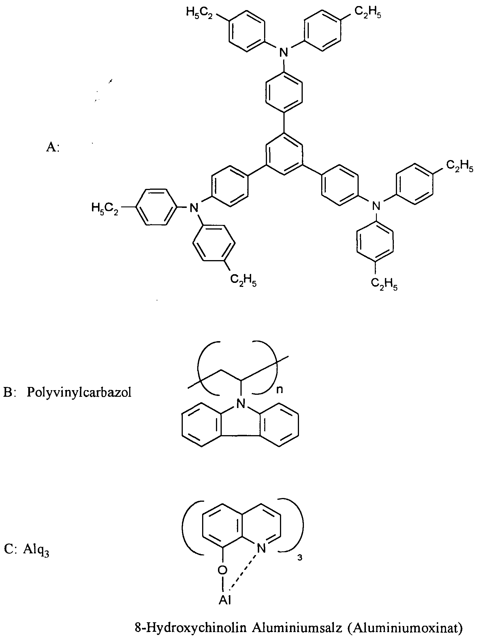
- Electroluminescent arrangement based on a blend system
- a 1% solution consisting of 1 part by weight A, 4 parts by weight B and 1 Part C by weight in dichloroethane is mixed with a commercial spin coater a speed of 400 / min on one with a lamellar electrode coated glass plate.
- the lamellar electrode consists of an approx. 100 nm thick ITO layer on which a 74 nm thick layer of polyethylene dioxythiophene / polystyrene sulfonic acid Na salt (Baytron P, Bayer AG, Leverkusen, Germany) was.
- the coating is carried out according to the information in EP-A 686 662. However the heat treatment described there was dispensed with and the substrate Annealed at 80 ° C under nitrogen for 1 h.
- the layer thickness of the blend system is 100 nm.
- the counter electrode is Mg / Ag in a ratio of 10: 1 through thermal code position upset.
- the arrangement After contacting and application of an electric field, the arrangement shows visually recognizable electroluminescence in the green spectral range from about 8 V.
- the brightness is 89 cd / m 2 at a current of 19.1 mA / cm 2 and a voltage of 17 V.
- the electronic levels of the arrangement are determined as follows. Work function comment ITO 4.7 eV [ID Parker] PEDT / PSS Baytron P 5.1 eV own measurement (Kelvin probe)
- Electroluminescent arrangement based on a blend system
- the lamellar electrode consists of a tin oxide layer on a 4 mm Flat glass on which a 74 nm thick layer of polyethylenedioxythiophene / polystyrene sulfonic acid Na salt had been hurled.
- the coating takes place according to the information in EP-A 686 662. However, attention has been paid to the one described there No heat treatment and the substrate at 80 ° C under nitrogen for 1 h annealed.
- the layer thickness of the hole-conducting layer is approximately 70 nm.
- An electron-conducting or emitting layer consisting of Alq 3 is evaporated onto this hole-conducting layer at 10 -6 mbar.
- the layer thickness is approx. 60 nm.
- a MgAg alloy in a ratio of 10: 1 is applied as the counter electrode by thermal code position.
- the system emits the green light.
- the brightness is 550 Cd / m 2 at a current of 14 mA / cm 2 and a voltage of 12 volts.
- ionization potentials or the highest occupied molecular bitals (HOMO) of typical organic hole conductors are in the range from 5.1 to 5.5 eV (see C. Adachi, K. Nagai, N. Tamoto, Appl. Phys. Lett. 66 ( 1995) 2679-2681).
Landscapes
- Physics & Mathematics (AREA)
- Chemical & Material Sciences (AREA)
- Engineering & Computer Science (AREA)
- Materials Engineering (AREA)
- Optics & Photonics (AREA)
- Spectroscopy & Molecular Physics (AREA)
- Electroluminescent Light Sources (AREA)
- Luminescent Compositions (AREA)
Abstract
Description
(Zinnoxid ist ein vergleichsweise kostengünstigeres Material, das ebenfalls transparent und elektrisch leitfähig ist. Zinnoxid hat jedoch eine niedrigere Elektronenaustrittsarbeit und wird deshalb in der Regel nicht eingesetzt.)

| Austrittsarbeit | Bemerkung | |
| ITO | 4,7 eV | [I.D. Parker] |
| PEDT/PSS Baytron P | 5,1 eV | eigene Messung (Kelvinsonde) |
Claims (4)
- Elektrolumineszierende Anordnung aus einem Substrat, einer Anode, einem elektrolumineszierenden Element und einer Kathode, wobei wenigstens eine der beiden Elektroden im sichtbaren Spektralbereich transparent ist und die Anode lamellar aus mindestens zwei dünnen Schichten aufgebaut ist, wobei die an den Träger angrenzende Schicht aus einem elektrisch leitfähigen, anorganischen Material mit einer beliebigen Elektronenaustrittsarbeit und die an das elektrolumineszierende Element angrenzende Schicht aus einem Material besteht, das elektrisch leitfähig ist und das sich aus einer Lösung heraus deponieren läßt.
- Elektrolumineszierende Anordnung gemaß Anspruch 1, dadurch gekennzeichnet, daß die an das elektrolumineszierende Element angrenzende Schicht eine Elektronenaustrittsarbeit von größer als 4 eV besitzt.
- Elektrolumineszierende Anordnung gemäß Anspruch 1 und 2, dadurch gekennzeichnet, daß es sich bei der an das elektrolumineszierende Element angrenzenden Schicht aus Polyethylendioxithiophen (PEDT)/Polystyrolsulfonsäure-Salz handelt.
- Verwendung der erfindungsgemäßen lamellaren Elektroden in elektrolumineszierenden Anordnungen.
Applications Claiming Priority (2)
| Application Number | Priority Date | Filing Date | Title |
|---|---|---|---|
| DE19627069A DE19627069A1 (de) | 1996-07-05 | 1996-07-05 | Elektrolumineszierende Anordnungen unter Verwendung von lamellaren Elektroden |
| DE19627069 | 1996-07-05 |
Publications (2)
| Publication Number | Publication Date |
|---|---|
| EP0817540A2 true EP0817540A2 (de) | 1998-01-07 |
| EP0817540A3 EP0817540A3 (de) | 2000-02-23 |
Family
ID=7798997
Family Applications (1)
| Application Number | Title | Priority Date | Filing Date |
|---|---|---|---|
| EP97110256A Withdrawn EP0817540A3 (de) | 1996-07-05 | 1997-06-23 | Eletrolumineszierende Anordnungen unter Verwendung von lamellaren Elektroden |
Country Status (4)
| Country | Link |
|---|---|
| EP (1) | EP0817540A3 (de) |
| JP (1) | JPH1092584A (de) |
| KR (1) | KR980013537A (de) |
| DE (1) | DE19627069A1 (de) |
Cited By (12)
| Publication number | Priority date | Publication date | Assignee | Title |
|---|---|---|---|---|
| DE19718859A1 (de) * | 1997-05-03 | 1998-11-05 | Technoplast Beschichtungsgesel | Leitfähige bedruckbare Bahnen aus Kunststoff |
| WO2000014173A1 (de) * | 1998-09-02 | 2000-03-16 | Bayer Aktiengesellschaft | Elektrolumineszierende anordnungen mit mehrkernigen metallkomplexen |
| FR2844136A1 (fr) * | 2002-09-03 | 2004-03-05 | Corning Inc | Materiau utilisable dans la fabrication de dispositifs d'affichage lumineux en particulier de diodes electroluminescentes organiques |
| US7250461B2 (en) | 2004-03-17 | 2007-07-31 | E. I. Du Pont De Nemours And Company | Organic formulations of conductive polymers made with polymeric acid colloids for electronics applications, and methods for making such formulations |
| US7670506B1 (en) | 2004-12-30 | 2010-03-02 | E. I. Du Pont De Nemours And Company | Photoactive compositions for liquid deposition |
| US8147962B2 (en) | 2004-04-13 | 2012-04-03 | E. I. Du Pont De Nemours And Company | Conductive polymer composites |
| US8216680B2 (en) | 2006-02-03 | 2012-07-10 | E I Du Pont De Nemours And Company | Transparent composite conductors having high work function |
| US8641926B2 (en) | 2003-04-22 | 2014-02-04 | E I Du Pont De Nemours And Company | Water dispersible polythiophenes made with polymeric acid colloids |
| USRE44853E1 (en) | 2005-06-28 | 2014-04-22 | E I Du Pont De Nemours And Company | Buffer compositions |
| US8845933B2 (en) | 2009-04-21 | 2014-09-30 | E I Du Pont De Nemours And Company | Electrically conductive polymer compositions and films made therefrom |
| US8945426B2 (en) | 2009-03-12 | 2015-02-03 | E I Du Pont De Nemours And Company | Electrically conductive polymer compositions for coating applications |
| US8945427B2 (en) | 2009-04-24 | 2015-02-03 | E I Du Pont De Nemours And Company | Electrically conductive polymer compositions and films made therefrom |
Families Citing this family (5)
| Publication number | Priority date | Publication date | Assignee | Title |
|---|---|---|---|---|
| DE10019888B4 (de) * | 2000-04-20 | 2011-06-16 | Schott Ag | Transparente elektronische Bauelementanordnung und Verfahren zu ihrer Herstellung |
| SG105534A1 (en) * | 2001-03-07 | 2004-08-27 | Bayer Ag | Multilayered arrangement for electro-optical devices |
| KR20060096980A (ko) | 2003-07-31 | 2006-09-13 | 미쓰비시 가가꾸 가부시키가이샤 | 화합물, 전하 수송 재료 및 유기 전계 발광 소자 |
| TWI275051B (en) | 2003-10-16 | 2007-03-01 | Pioneer Corp | Organic electroluminescence display panel |
| US8178215B2 (en) | 2004-12-10 | 2012-05-15 | Pioneer Corporation | Organic compound containing at least two carbazolyl-substituted phenyl structures; charge-transporting material and organic el element containing the compound |
Citations (4)
| Publication number | Priority date | Publication date | Assignee | Title |
|---|---|---|---|---|
| EP0643118A1 (de) * | 1993-09-09 | 1995-03-15 | Takakazu Yamamoto | El-Element brauchend Polythiophene |
| WO1995024056A1 (en) * | 1994-03-03 | 1995-09-08 | Uniax Corporation | Bilayer composite electrodes for diodes |
| EP0686662A2 (de) * | 1994-05-06 | 1995-12-13 | Bayer Ag | Leitfähige Beschichtungen |
| WO1996008047A2 (en) * | 1994-09-06 | 1996-03-14 | Philips Electronics N.V. | Electroluminescent device comprising a transparent structured electrode layer made from a conductive polymer |
-
1996
- 1996-07-05 DE DE19627069A patent/DE19627069A1/de not_active Withdrawn
-
1997
- 1997-06-23 EP EP97110256A patent/EP0817540A3/de not_active Withdrawn
- 1997-06-30 JP JP9187137A patent/JPH1092584A/ja active Pending
- 1997-07-04 KR KR1019970031120A patent/KR980013537A/ko not_active Application Discontinuation
Patent Citations (4)
| Publication number | Priority date | Publication date | Assignee | Title |
|---|---|---|---|---|
| EP0643118A1 (de) * | 1993-09-09 | 1995-03-15 | Takakazu Yamamoto | El-Element brauchend Polythiophene |
| WO1995024056A1 (en) * | 1994-03-03 | 1995-09-08 | Uniax Corporation | Bilayer composite electrodes for diodes |
| EP0686662A2 (de) * | 1994-05-06 | 1995-12-13 | Bayer Ag | Leitfähige Beschichtungen |
| WO1996008047A2 (en) * | 1994-09-06 | 1996-03-14 | Philips Electronics N.V. | Electroluminescent device comprising a transparent structured electrode layer made from a conductive polymer |
Non-Patent Citations (2)
| Title |
|---|
| GUSTAFSSON G ET AL: "FLEXIBLE LIGHT-EMITTING DIODES MADE FROM SOLUBLE CONDUCTING POLYMERS" NATURE,GB,MACMILLAN JOURNALS LTD. LONDON, Bd. 357, Nr. 6378, Seite 477-479 XP000574074 ISSN: 0028-0836 * |
| YANG Y ET AL: "POLYANILINE BILAYER COMPOSITE ELECTRODE FOR EFFICIENT POLYMER LIGHTEMITTING DIODES" MOLECULAR CRYSTALS AND LIQUID CRYSTALS SCIENCE AND TECHNOLOGY. SECTION A. MOLECULAR CRYSTALS AND LIQUID CRYSTALS,CH,GORDON AND BREACH PUBLISHERS, CH, Bd. 256, Seite 537-542 XP002066738 ISSN: 1058-725X * |
Cited By (19)
| Publication number | Priority date | Publication date | Assignee | Title |
|---|---|---|---|---|
| DE19718859A1 (de) * | 1997-05-03 | 1998-11-05 | Technoplast Beschichtungsgesel | Leitfähige bedruckbare Bahnen aus Kunststoff |
| DE19718859C2 (de) * | 1997-05-03 | 1999-08-26 | Technoplast Beschichtungsgesel | Leitfähige bedruckbare Bahnen aus Kunststoff |
| WO2000014173A1 (de) * | 1998-09-02 | 2000-03-16 | Bayer Aktiengesellschaft | Elektrolumineszierende anordnungen mit mehrkernigen metallkomplexen |
| US6534200B1 (en) | 1998-09-02 | 2003-03-18 | Bayer Aktiengesellshaft | Electroluminescent systems with polynulcear metal complexes |
| EP1573702A4 (de) * | 2002-09-03 | 2008-07-23 | Corning Inc | Material zur verwendung bei der herstellung von leuchtanzeigebauelementen |
| FR2844136A1 (fr) * | 2002-09-03 | 2004-03-05 | Corning Inc | Materiau utilisable dans la fabrication de dispositifs d'affichage lumineux en particulier de diodes electroluminescentes organiques |
| US7161171B2 (en) | 2002-09-03 | 2007-01-09 | Corning Incorporated | Material for use in the manufacturing of luminous display devices |
| EP1573702A2 (de) * | 2002-09-03 | 2005-09-14 | Corning Incorporated | Material zur verwendung bei der herstellung von leuchtanzeigebauelementen |
| US8641926B2 (en) | 2003-04-22 | 2014-02-04 | E I Du Pont De Nemours And Company | Water dispersible polythiophenes made with polymeric acid colloids |
| US7250461B2 (en) | 2004-03-17 | 2007-07-31 | E. I. Du Pont De Nemours And Company | Organic formulations of conductive polymers made with polymeric acid colloids for electronics applications, and methods for making such formulations |
| US8147962B2 (en) | 2004-04-13 | 2012-04-03 | E. I. Du Pont De Nemours And Company | Conductive polymer composites |
| US7670506B1 (en) | 2004-12-30 | 2010-03-02 | E. I. Du Pont De Nemours And Company | Photoactive compositions for liquid deposition |
| USRE44853E1 (en) | 2005-06-28 | 2014-04-22 | E I Du Pont De Nemours And Company | Buffer compositions |
| US8216680B2 (en) | 2006-02-03 | 2012-07-10 | E I Du Pont De Nemours And Company | Transparent composite conductors having high work function |
| US8273459B2 (en) | 2006-02-03 | 2012-09-25 | E I Du Pont De Nemours And Company | Transparent composite conductors having high work function |
| US8343630B2 (en) | 2006-02-03 | 2013-01-01 | E I Du Pont De Nemours And Company | Transparent composite conductors having high work function |
| US8945426B2 (en) | 2009-03-12 | 2015-02-03 | E I Du Pont De Nemours And Company | Electrically conductive polymer compositions for coating applications |
| US8845933B2 (en) | 2009-04-21 | 2014-09-30 | E I Du Pont De Nemours And Company | Electrically conductive polymer compositions and films made therefrom |
| US8945427B2 (en) | 2009-04-24 | 2015-02-03 | E I Du Pont De Nemours And Company | Electrically conductive polymer compositions and films made therefrom |
Also Published As
| Publication number | Publication date |
|---|---|
| EP0817540A3 (de) | 2000-02-23 |
| JPH1092584A (ja) | 1998-04-10 |
| KR980013537A (ko) | 1998-04-30 |
| DE19627069A1 (de) | 1998-01-08 |
Similar Documents
| Publication | Publication Date | Title |
|---|---|---|
| DE69710781T2 (de) | Elektrolumineszierende anordnungen mit elektrodenschutz | |
| EP0817540A2 (de) | Eletrolumineszierende Anordnungen unter Verwendung von lamellaren Elektroden | |
| DE69737866T2 (de) | Elektrodenabscheidung für organische lichtemittierende vorrichtungen | |
| DE69016345T2 (de) | Elektrolumineszierende anordnungen. | |
| DE69834259T2 (de) | Bipolare/ac lichtemittierende vorrichtungen mit variabler farbe | |
| EP1227529B1 (de) | Elektrolumineszierende Anordnungen | |
| DE69529512T2 (de) | Elektrolumineszente Vorrichtung mit einer Poly-3,4-Ethylen-Dioxythiophen-Schicht | |
| DE69422242T2 (de) | El-Element brauchend Polythiophene | |
| DE69724129T2 (de) | Lichtemittierende organische vorrichtungen mit verbesserter kathode | |
| DE69819270T2 (de) | Elektrolumineszente Vorrichtung | |
| DE10058578C2 (de) | Lichtemittierendes Bauelement mit organischen Schichten | |
| EP1564250B1 (de) | Polythiophenformulierungen zur Verbesserung von organischen Leuchtdioden | |
| EP0909464B1 (de) | Elektrolumineszierende anordnungen | |
| EP1929560B1 (de) | Neutralisierte anodenpufferschicht zur verbesserung der verarbeitung und leistungsfähigkeiten organischer lichtemittierender bauelemente und deren herstellungsmethode | |
| DE10191386B4 (de) | Organische Substanz/Polymer enthaltende Elektrolumineszenzvorrichtungen mit Einionenleiter | |
| EP2203944B1 (de) | Optoelektronische vorrichtung | |
| DE112009000486T5 (de) | Lösungsmittel für eine Druckzusammensetzung | |
| DE19832644C1 (de) | Organische lichtemittierende Dioden (OLED) mit Poly[2-methoxy-5-(2'-ethylhexyloxy)-1,4-phenylen-1,2-ethenylen-2,5-dimethoxy-1,4-phenylen-1,2-ethenylen] als Elektrolumineszenzmaterial | |
| DE19825737A1 (de) | Elektrolumineszierende Anordnungen mit N-Alkyl-2,2'-imino-bis-(8-hydroxychinolin)-Metallkomplexen | |
| DE19839947A1 (de) | Elektrolumineszierende Anordnungen mit Thiophencarboxylat-Metallkomplexen | |
| DE69423093T2 (de) | Elektrolumineszente vorrichtungen und verfahren unter verwendung von polythiophenen | |
| DE19839946A1 (de) | Elektrolumineszierende Anordnungen mit mehrkernigen Metallkomplexen | |
| DE102004010811B4 (de) | Polythiophenformulierungen zur Verbesserung von organischen Leuchtdioden | |
| DE112006000714T5 (de) | Organische Elektrolumineszenzvorrichtung | |
| WO1998054767A1 (de) | Leitfähiges schichtsystem und dessen verwendung in elektrolumineszierenden anordnungen |
Legal Events
| Date | Code | Title | Description |
|---|---|---|---|
| PUAI | Public reference made under article 153(3) epc to a published international application that has entered the european phase |
Free format text: ORIGINAL CODE: 0009012 |
|
| AK | Designated contracting states |
Kind code of ref document: A2 Designated state(s): CH DE ES FR GB LI NL SE |
|
| PUAL | Search report despatched |
Free format text: ORIGINAL CODE: 0009013 |
|
| AK | Designated contracting states |
Kind code of ref document: A3 Designated state(s): CH DE ES FR GB LI NL SE |
|
| RIC1 | Information provided on ipc code assigned before grant |
Free format text: 7H 05B 33/26 A, 7H 01L 51/20 B, 7H 05B 33/28 B |
|
| RAP1 | Party data changed (applicant data changed or rights of an application transferred) |
Owner name: ROBERT BOSCH GMBH Owner name: BAYER AG |
|
| 17P | Request for examination filed |
Effective date: 20000823 |
|
| AKX | Designation fees paid |
Free format text: CH DE ES FR GB LI NL SE |
|
| 17Q | First examination report despatched |
Effective date: 20010627 |
|
| STAA | Information on the status of an ep patent application or granted ep patent |
Free format text: STATUS: THE APPLICATION HAS BEEN WITHDRAWN |
|
| 18W | Application withdrawn |
Withdrawal date: 20010830 |