EP0809863B1 - Transistoren mit heissen ladungsträgern und verfahren zur herstellung - Google Patents
Transistoren mit heissen ladungsträgern und verfahren zur herstellung Download PDFInfo
- Publication number
- EP0809863B1 EP0809863B1 EP96937461A EP96937461A EP0809863B1 EP 0809863 B1 EP0809863 B1 EP 0809863B1 EP 96937461 A EP96937461 A EP 96937461A EP 96937461 A EP96937461 A EP 96937461A EP 0809863 B1 EP0809863 B1 EP 0809863B1
- Authority
- EP
- European Patent Office
- Prior art keywords
- semiconductor
- amorphous
- metal
- emitter
- silicon
- Prior art date
- Legal status (The legal status is an assumption and is not a legal conclusion. Google has not performed a legal analysis and makes no representation as to the accuracy of the status listed.)
- Expired - Lifetime
Links
Images
Classifications
-
- H—ELECTRICITY
- H10—SEMICONDUCTOR DEVICES; ELECTRIC SOLID-STATE DEVICES NOT OTHERWISE PROVIDED FOR
- H10D—INORGANIC ELECTRIC SEMICONDUCTOR DEVICES
- H10D48/00—Individual devices not covered by groups H10D1/00 - H10D44/00
- H10D48/30—Devices controlled by electric currents or voltages
- H10D48/32—Devices controlled by only the electric current supplied, or only the electric potential applied, to an electrode which does not carry the current to be rectified, amplified or switched
- H10D48/36—Unipolar devices
- H10D48/362—Unipolar transistors having ohmic electrodes on emitter-like, base-like, and collector-like regions, e.g. hot electron transistors [HET], metal base transistors [MBT], resonant tunnelling transistors [RTT], bulk barrier transistors [BBT], planar doped barrier transistors [PDBT] or charge injection transistors [CHINT]
-
- H10P30/204—
-
- H—ELECTRICITY
- H10—SEMICONDUCTOR DEVICES; ELECTRIC SOLID-STATE DEVICES NOT OTHERWISE PROVIDED FOR
- H10D—INORGANIC ELECTRIC SEMICONDUCTOR DEVICES
- H10D48/00—Individual devices not covered by groups H10D1/00 - H10D44/00
- H10D48/01—Manufacture or treatment
- H10D48/031—Manufacture or treatment of three-or-more electrode devices
- H10D48/032—Manufacture or treatment of three-or-more electrode devices of unipolar transistors having ohmic electrodes on emitter-like, base-like, and collector-like regions, e.g. hot electron transistors [HET], metal base transistors [MBT], resonant tunneling transistors [RTT], bulk barrier transistors [BBT], planar doped barrier transistors [PDBT] or charge injection transistors [CHINT]
-
- H10P30/214—
Definitions
- This invention relates to hot carrier transistors comprising a metal-semiconductor alloy base region between semiconductor emitter and collector regions. Particularly, but not exclusively, the invention may provide a thin-film hot electron transistor having a metal-silicide base region. The invention also relates to methods of manufacturing such transistors.
- United States Patent US-A-4,492,971 describes an improved hot electron transistor comprising a metal-silicide base region between silicon emitter and collector regions.
- This transistor has an essentially monocrystalline structure comprising a monocrystalline silicon layer forming an emitter region epitaxially grown on a thin monocrystalline metal silicide layer which forms the base region and which is epitaxially grown on a monocrystalline silicon substrate forming the collector region.
- This composite structure has an essentially continuous single crystal lattice between the three layers.
- the thickness of the metal-silicide base layer is thin (typically 4, 6 or 8 nm) so as to be small compared with the hot electron scattering length in this silicide base material and is made a multiple of the quantum mechanical transmission probability factor.
- the emitter-base and base-collector junctions of the transistor are formed by Schottky barriers between the metal silicide base and the silicon emitter and collector regions.
- QM quantum mechanical transmission probability
- United States Patents US-A-4,707,197, US-A-4,837,174, US-A-5,236,872, and US-A-5,290,715 describe various forms and variations of such a metal-silicide base transistor, and various methods for the manufacture of such transistors.
- the last three of these US Patents discloses ion implantation methods for forming the metal-silicide base region.
- the implanted structure is annealed by a prolonged heat treatment at a high temperature, for example, between 575°C and 1000°C in order to restore the crystalline quality of the emitter, base and collector regions.
- the silicon material is first rendered amorphous by implantation (for example of silicon ions), thereby providing a high solubility for the metal ions which are subsequently implanted to provide the silicide.
- the subsequent heat treatment at a high temperature is then carried out to form the silicide as a layer with a thickness smaller than that of the amorphous layer originally formed.
- the present invention adopts a completely opposite approach in order to provide a hot carrier transistor comprising a silicon-rich metal-silicide base region with an adequate cumulative quantum mechanical transmission probability.
- a hot carrier transistor comprising a metal-semiconductor alloy base region located between semiconductor emitter and collector regions and forming Schottky barriers with the emitter and collector regions is characterised in that the emitter and collector regions comprise hydrogenated amorphous semiconductor material adjoining an intermediate semiconductor-rich amorphous metal-semiconductor alloy layer which provides the base region.
- the hot carrier transistor of the present invention is based on amorphous semiconductor material for the emitter, base and collector regions. Hydrogenation of this material reduces to an acceptable level the high density of defect states which naturally occur in amorphous semiconductor material and which otherwise lead to a high density of carrier traps at deep energy levels in the energy band gap.
- the hydrogen (which may be introduced either during the deposition of the material or in a subsequent hydrogenation process) attaches itself to unsaturated bonds throughout the bulk of the amorphous semiconductor material where the defect states occur. By this means, adequate charge-carrier transport through the emitter and collector regions can be achieved.
- the provision of the hydrogen in the amorphous semiconductor material is found to facilitate the formation therein or thereon of an amorphous metal-semiconductor alloy layer which can be very rich in the semiconductor element (i.e having a very dilute metal concentration) while still forming a Schottky barrier with the adjoining amorphous semiconductor region.
- the semiconductor-rich metal-semiconductor alloy base region of the amorphous transistor structure in accordance with the present invention provides an important difference with respect to the emitter and collector barriers, as compared with the prior art approaches.
- hot carriers from the emitter of such a transistor in accordance with the present invention are presented with a range of quantum mechanical environments due to the amorphous nature of the base region which leads to spatial variations in wavelength and effective mass.
- the current transport through this base region will therefore be spatially self-selective, in that the hot carriers will tend to pass through those areas where there is a resonance between the wave function, the barrier heights and the base width.
- the preferred routes for the hot carriers in a silicon example in accordance with the invention will be via a silicon environment in the amorphous silicon-rich base region, from the emitter region to the collector region.
- the emitter and collector regions each comprise undoped or only lightly-doped hydrogenated amorphous material adjoining the intermediate silicide base layer.
- This undoped or lightly doped semiconductor material provides good electrical separation of the emitter and collector regions and facilitates the achievement of satisfactory barrier heights for emitter and collector Schottky barriers.
- the doping concentration is increased then more defects are generally generated in the amorphous semiconductor material and the leakage current across the Schottky barrier increases.
- a hot carrier transistor in accordance with the present invention is eminently suitable for fabrication using known silicon thin-film technology processes, and such a thin-film silicon hot carrier transistor may form part of a large-area electronic device manufactured using silicon thin-film technology.
- silicon-rich amorphous silicide layers in a hydrogenated amorphous silicon material is described in the article "Interaction in the Cr/amorphous-silicon system" by Y Masaki et al in Journal of Applied Physics, Vol 77, No 6, 15 March 1995, pp 2474-2478.
- Thin-film technology based on germanium is also known and may be used instead of (or in addition to) silicon thin-film technology to fabricate a thin-film hot carrier transistor in accordance with the invention.
- a more efficient hot-hole transistor in accordance with the invention may be produced with germanium thin-film technology rather than silicon thin-film technology.
- a method of manufacturing an electronic device comprising a hot carrier transistor in accordance with a first aspect of the invention, characterised by steps which include depositing at least one amorphous semiconductor thin film for the emitter and collector regions, hydrogenating the amorphous thin-film material, and introducing metal atoms into a part of the amorphous semiconductor thin-film material to form a semiconductor-rich amorphous metal-semiconductor alloy layer for the base region, this layer being maintained at a temperature below 400°C during the manufacture.
- steps which include depositing at least one amorphous semiconductor thin film for the emitter and collector regions, hydrogenating the amorphous thin-film material, and introducing metal atoms into a part of the amorphous semiconductor thin-film material to form a semiconductor-rich amorphous metal-semiconductor alloy layer for the base region, this layer being maintained at a temperature below 400°C during the manufacture.
- steps which include depositing at least one amorphous semiconductor thin film for the emitter and collector regions
- the amorphous semiconductor-rich metal-semiconductor alloy layer may be formed by implanting atoms of at least one metal (for example from the group comprising chromium, cobalt, nickel, iron, iridium and platinum) within a part of the amorphous semiconductor thin-film material, at least adjoining parts of which may provide the emitter and collector regions. Ion implantation permits very precise control of the dose of metal atoms introduced into the amorphous semiconductor material to form the semiconductor-rich metal-semiconductor alloy.
- at least one metal for example from the group comprising chromium, cobalt, nickel, iron, iridium and platinum
- the semiconductor-rich amorphous metal-semiconductor alloy may be formed between first and second amorphous semiconductor thin films by depositing metal on the first amorphous film introducing metal atoms from the deposited metal into the surface of the first film to form a semiconductor-rich amorphous interface layer (for example having a semiconductor content in excess of 90% over a thickness of less than 10nm), etching away the remaining metal from the interface layer, and depositing the second amorphous semiconductor thin film on the interface layer. Because this second semiconductor film is provided after forming the alloy interface layer, the composition and layer structure of the second semiconductor film can be controlled more independently of the alloy formation process steps.
- the first semiconductor film may provide the emitter region, and the second semiconductor film may provide the collector region.
- the first semiconductor film can be advantageous for the collector region, and the second semiconductor film to provide the emitter region.
- the second film providing the emitter region may be of a semiconductor-rich alloy material having a wider energy bandgap, so as to improve the transistor efficiency.
- At least one metal from the group comprising chromium, cobalt, nickel, iron, iridium and platinum may be used to form a metal-silicide as the alloy in the amorphous base layer in a manner compatible with known hydrogenated amorphous silicon thin-film technology.
- a dopant may also be included in the base layer, for example phosphorus, antimony or boron in a silicon-rich base layer.
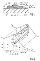
- Figures 1 and 2 illustrate a hot-electron transistor constructed with silicon thin-film technology in accordance with the present invention.
- the transistor comprises a metal-silicide base region 1 between silicon emitter and collector regions 2 and 3 respectively.
- the emitter and collector regions 2 and 3 are each of hydrogenated amorphous silicon material (a-Si:H) adjoining an intermediate silicon-rich amorphous silicide layer (a-Si 1-x M x :H) which provides the base region 1.
- the emitter and collector regions 2 and 3 comprise an undoped or lightly doped part 2a and 3a respectively, and a heavily donor-doped part 2b and 3b respectively.
- the undoped or lightly doped hydrogenated amorphous silicon parts 2a,3a (i a-Si:H) (hereinafter simply referred to as "undoped" parts) adjoin the intermediate silicon-rich amorphous silicide layer 1 and are designated by i in Figures 1 and 2 to indicate intrinsic or very low conductivity.
- the heavily donor-doped hydrogenated amorphous silicon parts 2b,3b (n+ a-Si:H) are designated by n+ to designate their high n-type conductivity. These donor-doped parts 2b,3b are contacted by respective emitter and collector electrodes 12,13 of the transistor.
- the intermediate silicon-rich amorphous silicide base layer 1 (a-Si 1-x M x :H) is contacted by a base electrode 11.
- Figure 1 illustrates the thin-film transistor fabricated on an insulating substrate 10 of a glass or other low-cost insulating material.
- This substrate 10 may form part of a large-area thin-film electronic device, for example a thin-film circuit plate of a flat-panel display or large-area image sensor.
- Hot carrier transistors are also sometimes termed ballistic transistors. Current flow through a hot carrier transistor is by hot majority charge-carriers 21 of one conductivity type in the base region 1, from the emitter region 2 to the collector region 3. Hot charge-carriers are not in thermal equilibrium with the semiconductor material. Thus, the average energy of hot electrons is considerably more than a few k.T above the average energy of electrons in equilibrium with the semiconductor material, where k and T are the Boltzmann constant and the material temperature respectively. At room temperature k.T is about 25meV. The electron mean free path in the silicide base 1 at room temperature exceeds the thickness of the silicide base region 1.
- amorphous hot electron transistors can be designed for operation at high frequencies, they do permit the provision in a large-area thin-film technology electronic device of transistors having different characteristics from the thin-film field-effect transistors (TFTs) conventionally formed in such devices.
- TFTs have a high input impedance at an insulated gate electrode
- amorphous hot carrier transistors in accordance with the present invention can provide transistor characteristics with a low input impedance at their base electrode 11.
- Figure 2 illustrates The new and advantageous nature of ballistic transport of the hot charge carriers 21 across the silicon-rich amorphous silicide base layer 1 of a hot carrier transistor in accordance with the present invention.
- Figure 2 illustrates local variations which occur in this quantum mechanical environment in a transistor in accordance with the present invention, both in the direction of thickness x and in the sideways direction z.
- Suitable metals M for forming the silicon-rich amorphous silicide alloy a-Si 1-x M x may be selected from, for example, the group comprising Cr, Co, Ni, Fe, Ir and Pt. These metal atoms introduced into the amorphous silicon material (a-Si) appear to be located randomly through the silicon-rich material, although at least some of these metal atoms may group together with neighbouring silicon atoms to form metal-silicide molecules distributed in the amorphous material, for example, with molecular bonds such as CrSi 2 , CoSi 2 , NiSi 2 , FeSi 2 , IrSi 3 and PtSi.
- the amorphous alloy base region 1 may be regarded as an interface layer having a silicon content which is typically in excess of 90% over a thickness which is typically less than 10nm (nanometres).
- this amorphous interface layer 1 may have a similar composition to that of the Cr/a-silicon system described in the Masaki et al article.
- the silicide-metal M may be Cr
- the compositional ratio of Cr to Si in the amorphous interface layer formed by deposition thereon of a chromium layer may be about 5%, i.e the composition of the interface layer may be Cr 5 Si 95 :H.
- Such a Cr 5 Si 95 :H layer can be moderately conducting, for example with a resistivity of about 10 -3 ⁇ cm. It seems likely that its conducting properties arise from the close proximity of the individual metal atoms in the amorphous layer 1. As described on a microscopic scale, the silicide appears to be continuous in the z direction in order to exhibit the observed conducting properties. Thus, although the amorphous silicide layer 1 may appear to have a thickness in the range of 5nm to 10nm it seems likely that the metal silicon clusters are concentrated more closely together to form much narrower localised silicide sections of the base region, the thickness x of which varies randomly on the atomic scale as x 1 ,x 2 etc in the direction z. It is this spatial variation of the metal distribution in the silicon-rich alloy in both the x and z directions which gives rise to the above-mentioned range of quantum mechanical environments.
- a silicon-rich amorphous silicide for the base layer 1 provides Si-Si bond arrangements in the base region 1 that are similar to the Si-Si bond arrangements in the amorphous silicon emitter and collector regions 2 and 3.
- quantum mechanical reflections of the hot electrons 21 at the base-collector silicide-silicon hetero-junction are reduced, because the preferred routes for the hot electrons 21 will be via a silicon environment from the emitter region 2 to the collector region 3.
- the reduction of these quantum mechanical reflections improves the collector efficiency of the transistor.
- this alloy layer 1 In order to improve further the conductivity of this silicon-rich base region 1, it is advantageous to also provide this alloy layer 1 with dopant determining the same conductivity type as that of the hot carriers through the base region 1.
- donor dopant such as, for example, phosphorus or antimony
- this doped semiconductor-rich metal-semiconductor alloy layer 1 is formed on the collector region 3, it can be advantageous for the dopant to penetrate also the part 3a of the collector region at least adjoining the base region 1.
- collector efficiency can be increased by having a slightly lower collector barrier (compared with the emitter barrier) as a result of lightly doping the collector region part 3a at the base region 1 while having an undoped emitter region part 2a.
- Amorphous silicon material naturally has a high density of defect states, mainly due to silicon dangling bonds. Hydrogenation of this material reduces to an acceptable level this density of defect states and so reduces to an acceptable level the associated density of deep energy levels in the energy band gap of the amorphous silicon material.
- the hydrogen in the material attaches itself to the dangling bonds throughout the bulk of the material where the defect states occur, thereby permitting adequate electron transport through the emitter and collector regions 2 and 3.
- the alloy base layer 1 is being formed on and/or in one of these regions 2 and 3, the hydrogen content of this region 2,3 also appears to play a significant role in achieving the desired highly-silicon-rich nature of the layer 1.
- the hydrogenation of the amorphous silicon material may occur during the deposition of the material, for example when the material is deposited by plasma-enhanced chemical-vapour deposition (PECVD) using SiH 4 . However, the hydrogenation may be carried out subsequently, for example by exposing the deposited amorphous silicon material to a hydrogen plasma.
- PECVD plasma-enhanced chemical-vapour deposition
- the process parameters for controlling the hydrogen content of amorphous silicon material are known, for example as described in the Masaki et al article.
- the hot electron transistor of Figures 1 and 2 may be fabricated using known amorphous silicon thin-film technologies.
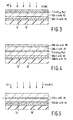
- Figures 3 and 4 illustrate one such example.
- an electrode film 13 is first deposited and patterned on the insulating substrate 10.
- the electrode film 13 may be of a metal such as, for example, chromium.
- Amorphous silicon material is then deposited by, for example, PECVD on the patterned electrode film 13 on the substrate 10.
- this amorphous silicon material comprises an undoped film 30a on a film 30b heavily doped with arsenic or another suitable donor dopant.
- the amorphous silicon material 30 may be deposited at a temperature below 300°C, for example at about 250°C.
- the hydrogenation step may be carried out during the deposition.
- the hydrogen content of this silicon material 30a and 30b may be, for example, typically 20%.
- These films 30a and 30b may provide the collector region 3 of the transistor and typically may have thicknesses of 0.5 ⁇ m and 0.1 ⁇ m respectively.
- Figure 3 illustrates the formation of the silicon-rich amorphous silicide layer 1 in a subsequent stage of the manufacture.
- the layer 1 is formed by depositing a layer 41 of metal M on the first amorphous silicon film 30a,30b and then introducing metal atoms from the deposited metal M into the surface of the amorphous silicon film 30a.
- Recoil implantation for example as described in United States Patent US-A-3,747,203 (our reference PHB 32012), may be used. The whole contents of US-A-3,747,203 are hereby incorporated herein as reference material.
- the layer 41 of deposited metal M may be bombarded with energetic ions 50, for example of xenon, argon or another inert gas, so that metal atoms M are introduced into the surface layer 1 by recoil from the implanted ions 50 in the layer 41.
- ions 50 for example of xenon, argon or another inert gas
- a step of heating the deposited metal M at a temperature below 400°C or 300°C may be carried out to introduce the metal atoms M in to the surface of the film 30a and so to form the silicon-rich alloy amorphous interface layer.
- Process parameters similar to those described in the Masaki article may be employed.
- the resulting silicide interface layer 1 has a silicon content in excess of 90% over a thickness of less than 10nm.
- the remaining metal layer 41 is etched away from the interface layer 1.
- a second amorphous silicon thin-film 20a,20b is then deposited by, for example, PECVD on the exposed interface layer 1. In this way the silicide layer 1 is sandwiched between first and second amorphous silicon thin-films 20 and 30.
- the resulting structure is illustrated in Figure 4.
- This metal film may be of, for example, chromium.
- Figures 1 and 3 show only an area of the device substrate 10 where the hot electron transistor of Figures 1 and 2 is formed.
- other circuit elements are generally formed on other areas of the substrate 10, for example conventional TFTs.
- a TFT of the known so-called "staggered" type may be formed from the films 30a,30b,13 at these other areas of the substrate 10.
- the films 30b and 13 at these other areas may be patterned to form source and drain electrodes of the TFT before depositing the undoped film 30a (i a-Si:H).
- the film 30a may be re-exposed at the TFT areas by etching away the layers 1,20a and 20b at these areas.
- a dielectric layer and a metal gate may then be deposited in known manner on the exposed film area 30a to form an insulated gate of the TFT, whose channel region is provided by the film 30a.
- the individual TFT body is formed from the films 30a and 30b by etching, and metal-film connection tracks are provided between the individual circuit elements on the substrate 10.
- FIG. 5 One such modification is illustrated in Figure 5 in which the silicon-rich amorphous metal-silicon alloy layer 1 is formed by direct ion implantation.
- the doped amorphous silicon film 30b is deposited on the patterned electrode film 13 on the substrate 10 as in Figure 3.
- a thicker undoped amorphous silicon film 23a i a-Si:H is then deposited, from which the emitter part 2a and at least a portion of the collector part 3a will subsequently be formed.
- Figure 5 illustrates the stage in which ions 51 of at least one metal M are implanted within a part of the amorphous silicon thin-film material 23a for providing the thin silicide layer 1.
- the actual formation of the silicide occurs when the implanted layer is annealed by heating at a temperature below 350°C. This annealing treatment may be carried out during the ion implantation or subsequently.
- Suitable metals for the ion implantation are, for example, chromium, cobalt, nickel, iron, iridium and platinum. Silicide layers 1 having very low resistivities can be formed in this way.
- a resistivity of about 0.2 x 10 -3 ⁇ cm can be obtained by implanting cobalt in a-Si:H at room temperature.
- dopant ions 51 may also be implanted in the silicon-rich metal-silicon alloy layer 1 to increase its conductivity.
- phosphorus ions 51 or antimony ions 51 may also be implanted.
- This donor doping of the layer 1 may also be used to provide a light donor doping of the collector region part 3a (23a in Figure 5), thereby permitting the collector barrier to be slightly lower than the emitter barrier for this transistor.
- the remaining thickness of the undoped film 20a may be deposited, and then the heavily doped amorphous silicon film 20b is deposited to form a layer structure similar to that of Figure 4. This layer structure is then further processed as for that of Figure 4 to complete the hot carrier transistor of Figures 1 and 2.
- the silicon-rich metal-silicon alloy interface layer 1 of Figures 3 and 4 may also be doped with phosphorus or antimony, i.e with dopant determining the same conductivity type as that of the hot carriers (electrons) through the transistor base region 1. This may be effected by implantation of very low energy dopant ions after removing the remaining metal film 41 of Figure 3 or by implantation of more energetic dopant ions when the metal film 41 is still present on the surface.
- the whole of the emitter region part 2a (20a) may be deposited to have different material properties from those of the collector region part 3a (30a).
- the emitter region 2 may comprise a hydrogenated amorphous semiconductor alloy material having a wider energy bandgap than that of the hydrogenated amorphous semiconductor material (a-Si:H) of the collector region 3.
- the semiconductor alloy may be based on the same semiconductor element as the collector region 3 and the base region 1, so maintaining a relatively simple manufacturing technology.
- the emitter region films 20a and 20b may be of silicon-rich amorphous silicon carbide (a-SiC y :H) or amorphous silicon-rich silicon-nitride (a-SiN y :H).
- the emitter comprises an undoped or lightly-doped semiconductor part 2a adjacent the metal-semiconductor alloy base region 1, and a heavily donor-doped semiconductor part 2b adjacent a metal electrode 12.
- a thin dielectric layer for example SiO 2 or Si 3 N 4
- the emitter may be an MIS structure ( m etal- i nsulator- s emiconductor) comprising a metal electrode 12, an insulating film 2b and an undoped or lightly-doped hydrogenated amorphous semiconductor part 2 which forms a Schottky barrier with the metal-semiconductor alloy base region 1.
- MIS structure m etal- i nsulator- s emiconductor
- the ion implantation step illustrated in Figure 5 is carried out into amorphous-silicon thin-film material 23a on an insulating substrate 10.
- an amorphous-silicon hot electron transistor in accordance with the present invention may be formed by a similar ion implantation processes into monocrystalline silicon material 23a epitaxially grown on a monocrystalline substrate.
- the amorphous silicon material of the base, emitter and collector regions 1 to 3 can be formed by ion implantation damage of the silicon crystal lattice.
- This amorphous silicon material may be hydrogenated by heating to, for example, about 300°C in a hydrogen plasma.
- Figure 1 illustrates the formation of the base electrode connection by locally removing the amorphous silicon film 2 from the amorphous silicide layer 1.
- the base electrode 11 may be of metal alloyed at low temperature through the thickness of the amorphous silicon thin-film 2 to form a metal-rich region contacting the silicide base region 1.
- FIGS 1 to 5 have illustrated the construction of a hot electron transistor in accordance with the present invention.
- hot hole transistors may also be fabricated in accordance with the present invention, by replacing the donor-doped thin-film material 2b and 3b with p-type material.
- Boron is a suitable acceptor dopant for hydrogenated amorphous silicon material.
- An amorphous germanium thin-film technology (based on a-Ge:H) may be used for a hot hole transistor, rather than the a-Si:H technology described in all the embodiments so far.
Landscapes
- Physics & Mathematics (AREA)
- Bipolar Transistors (AREA)
- High Energy & Nuclear Physics (AREA)
- Engineering & Computer Science (AREA)
- Health & Medical Sciences (AREA)
- Toxicology (AREA)
- Condensed Matter Physics & Semiconductors (AREA)
- General Physics & Mathematics (AREA)
- Manufacturing & Machinery (AREA)
- Computer Hardware Design (AREA)
- Microelectronics & Electronic Packaging (AREA)
- Power Engineering (AREA)
Claims (10)
- Transistor mit heißen Ladungsträgern mit einem Basisgebiet aus einer Metall-Halbleiterlegierung zwischen dem Halbleiter-Emittergebiet und dem Halbleiter-Kollektorgebiet, wobei Schottky-Übergänge mit dem Emittergebiet sowie dem Kollektorgebiet gebildet werden, dadurch gekennzeichnet, dass das Emittergebiet und das Kollektorgebiet ein hydriertes amorphes Halbleitermaterial umfasst, das an eine zwischenliegende an Halbleitermaterial reiche amorphe Metall-Halbleiterlegierungsschicht grenzt, die das Basisgebiet bildet.
- Transistor mit heißen Ladungsträgern nach Anspruch 1, weiterhin dadurch gekennzeichnet, dass das Emittergebiet nicht dotiertes hydriertes amorphes Siliziummaterial enthält, das an eine zwischenliegende an Halbleitermaterial reiche amorphe Silizidschicht grenzt, die das Basisgebiet bildet.
- Transistor mit heißen Ladungsträgern nach Anspruch 2, weiterhin dadurch gekennzeichnet, dass die an Silizium reiche amorphe Silizidschicht, die das Basisgebiet bildet, auf einer Schnittstelle zwischen den beiden Dünnfilmen aus hydriertem amorphem Silizium bzw. aus dem Emittergebiet und dem Kollektorgebiet als Schnittstellenschicht, und dass diese Schnittstellenschicht einen Siliziuminhalt über 90% hat über eine Dicke von weniger als 10 nm.
- Transistor mit heißen Ladungsträgern nach Anspruch 2 oder 3, weiterhin dadurch gekennzeichnet, dass wenigstens ein Metall aus der Gruppe mit Chrom, Kobalt, Nickel, Eisen, Iridium und Platin das Metallsilizid in der amorphen Silizidschicht bildet.
- Transistor mit heißen Ladungsträgern nach einem der vorstehenden Ansprüche, weiterhin dadurch gekennzeichnet, dass das Emittergebiet ein hydriertes amorphes Halbleiterlegierungsmaterial mit einem breiteren Energiebandabstand als der des hydrierten amorphen Halbleitermaterials des Kollektorgebietes.
- Transistor mit heißen Ladungsträgern nach einem der vorstehenden Ansprüche, weiterhin dadurch gekennzeichnet, dass ein Dotierungsmittel, das denselben Leitungstyp bestimmt wie der der heißen Ladungsträger durch das Basisgebiet, in der an Halbleitermaterial reichen amorphen Metall-Halbleiterlegierungsschicht vorhanden ist, die das Basisgebiet liefert.
- Transistor mit heißen Ladungsträgern nach einem der vorstehenden Ansprüche, weiterhin dadurch gekennzeichnet, dass das Emittergebiet und das Kollektorgebiet je ein durch Donatoren dotiertes Gebiet aus dem hydrierten amorphen Halbleitermaterial enthalten, das durch betreffende Emitter- und Kollektorelektroden kontaktiert wird, wobei der Transistor ein Schottky-Transistor ist.
- Verfahren zum Herstellen einer elektronischen Anordnung mit einem Transistor mit heißen Ladungsträgern nach einem der vorstehenden Ansprüche, gekennzeichnet durch Verfahrensschritte die Folgendes umfassen: das Ablagern wenigstens eines amorphen Halbleiter-Dünnfilms für das Emittergebiet und das Kollektorgebiet, das Hydrieren des amorphen Dünnfilm-Materials und das Einführen von Metallatomen in einen Teil des amorphen Halbleiter-Dünnfilm-Materials zum Bilden einer an Halbleitermaterial reichen, amorphen Schicht aus einer Metall-Halbleiter-Legierung für das Basisgebiet, wobei diese Schicht während der Fertigung auf einer Temperatur unterhalb 400°C gehalten wird.
- Verfahren nach Anspruch 8, weiterhin dadurch gekennzeichnet, dass die an Halbleitermaterial reiche, amorphe Metall-Halbleiterlegierungsschicht durch Ablagerung von Metall auf dem ersten amorphen Halbleiterfilm zwischen dem ersten und dem zweiten amorphen Halbleiter-Dünnfilm gebildet wird, wobei Metallatome aus dem abgelagerten Metall in die Oberfläche des ersten amorphen Halbleiterfilms eingeführt werden zum Bilden einer an Halbleitermaterial reichen amorphen Schnittstellenschicht mit einem Halbleiterinhalt über 90% über eine Dicke von weniger als 10 nm, wobei das restliche Metall von der Schnittstellenschicht weggeätzt wird und wobei der zweite amorphe Halbleiter-Dünnfilm auf der Schnittstellenschicht abgelagert wird.
- Verfahren nach Anspruch 9, weiterhin dadurch gekennzeichnet, dass die Metallatome in die Oberfläche des ersten amorphen Halbleiterfilms dadurch eingeführt werden, dass das abgelagerte Metall auf eine Temperatur unterhalb 400°C erhitzt wird oder durch Rückstoß bei der Implantation von Ionen in dem abgelagerten Metall.
Applications Claiming Priority (3)
| Application Number | Priority Date | Filing Date | Title |
|---|---|---|---|
| GBGB9525784.6A GB9525784D0 (en) | 1995-12-16 | 1995-12-16 | Hot carrier transistors and their manufacture |
| GB9525784 | 1995-12-16 | ||
| PCT/IB1996/001294 WO1997022999A1 (en) | 1995-12-16 | 1996-11-25 | Hot carrier transistors and their manufacture |
Publications (2)
| Publication Number | Publication Date |
|---|---|
| EP0809863A1 EP0809863A1 (de) | 1997-12-03 |
| EP0809863B1 true EP0809863B1 (de) | 2002-07-10 |
Family
ID=10785568
Family Applications (1)
| Application Number | Title | Priority Date | Filing Date |
|---|---|---|---|
| EP96937461A Expired - Lifetime EP0809863B1 (de) | 1995-12-16 | 1996-11-25 | Transistoren mit heissen ladungsträgern und verfahren zur herstellung |
Country Status (7)
| Country | Link |
|---|---|
| US (1) | US5744817A (de) |
| EP (1) | EP0809863B1 (de) |
| JP (1) | JPH11501165A (de) |
| KR (1) | KR19980702229A (de) |
| DE (1) | DE69622258T2 (de) |
| GB (1) | GB9525784D0 (de) |
| WO (1) | WO1997022999A1 (de) |
Families Citing this family (20)
| Publication number | Priority date | Publication date | Assignee | Title |
|---|---|---|---|---|
| US7005702B1 (en) * | 2000-05-05 | 2006-02-28 | International Rectifier Corporation | IGBT with amorphous silicon transparent collector |
| US6429129B1 (en) | 2000-06-16 | 2002-08-06 | Chartered Semiconductor Manufacturing Ltd. | Method of using silicon rich carbide as a barrier material for fluorinated materials |
| US7173275B2 (en) * | 2001-05-21 | 2007-02-06 | Regents Of The University Of Colorado | Thin-film transistors based on tunneling structures and applications |
| US7084423B2 (en) | 2002-08-12 | 2006-08-01 | Acorn Technologies, Inc. | Method for depinning the Fermi level of a semiconductor at an electrical junction and devices incorporating such junctions |
| US6833556B2 (en) | 2002-08-12 | 2004-12-21 | Acorn Technologies, Inc. | Insulated gate field effect transistor having passivated schottky barriers to the channel |
| US20040206951A1 (en) * | 2003-04-18 | 2004-10-21 | Mirabedini Mohammad R. | Ion implantation in channel region of CMOS device for enhanced carrier mobility |
| US6982229B2 (en) * | 2003-04-18 | 2006-01-03 | Lsi Logic Corporation | Ion recoil implantation and enhanced carrier mobility in CMOS device |
| JP5182775B2 (ja) * | 2006-03-22 | 2013-04-17 | 国立大学法人大阪大学 | トランジスタ素子及びその製造方法、電子デバイス、発光素子並びにディスプレイ |
| US8642413B2 (en) * | 2006-09-14 | 2014-02-04 | Intel Corporation | Formation of strain-inducing films using hydrogenated amorphous silicon |
| WO2009129391A2 (en) * | 2008-04-17 | 2009-10-22 | Applied Materials, Inc. | Low temperature thin film transistor process, device property, and device stability improvement |
| JP5370810B2 (ja) * | 2008-09-19 | 2013-12-18 | 富士電機株式会社 | トランジスタ素子およびその製造方法 |
| US8436337B2 (en) | 2009-05-12 | 2013-05-07 | The State of Oregon Acting By and Through The State Board of Higher Education on Behalf of Oregon State Unitiversity | Amorphous multi-component metallic thin films for electronic devices |
| GB2526950B (en) | 2011-11-23 | 2016-04-20 | Acorn Tech Inc | Improving metal contacts to group IV semiconductors by inserting interfacial atomic monolayers |
| CN105264618B (zh) | 2012-11-12 | 2018-06-05 | 俄勒冈州立大学 | 非晶金属薄膜非线性电阻器 |
| US9312370B2 (en) * | 2014-06-10 | 2016-04-12 | Globalfoundries Inc. | Bipolar transistor with extrinsic base region and methods of fabrication |
| US9620611B1 (en) | 2016-06-17 | 2017-04-11 | Acorn Technology, Inc. | MIS contact structure with metal oxide conductor |
| JP7068265B2 (ja) * | 2016-07-07 | 2022-05-16 | アモルフィックス・インコーポレイテッド | アモルファス金属ホットエレクトロントランジスタ |
| DE112017005855T5 (de) | 2016-11-18 | 2019-08-01 | Acorn Technologies, Inc. | Nanodrahttransistor mit Source und Drain induziert durch elektrische Kontakte mit negativer Schottky-Barrierenhöhe |
| JP2021520060A (ja) | 2018-03-30 | 2021-08-12 | アモルフィックス・インコーポレイテッド | アモルファス金属薄膜トランジスタ |
| KR102892416B1 (ko) | 2020-06-12 | 2025-11-28 | 아모르픽스, 인크 | 비선형 컴포넌트를 포함하는 전자 디바이스용 회로 |
Family Cites Families (7)
| Publication number | Priority date | Publication date | Assignee | Title |
|---|---|---|---|---|
| BE759058A (de) * | 1969-11-19 | 1971-05-17 | Philips Nv | |
| US4492971A (en) * | 1980-06-05 | 1985-01-08 | At&T Bell Laboratories | Metal silicide-silicon heterostructures |
| US4707197A (en) * | 1984-08-02 | 1987-11-17 | American Telephone And Telegraph Company, At&T Bell Laboratories | Method of producing a silicide/Si heteroepitaxial structure, and articles produced by the method |
| SE454309B (sv) * | 1986-08-29 | 1988-04-18 | Stiftelsen Inst Mikrovags | Forfarande att framstella tunna ledande eller halvledande skikt inbeddade i kisel medelst implantering av metallatomer |
| JPS6437057A (en) * | 1987-07-15 | 1989-02-07 | Ibm | Thin film field effect transistor |
| US5236872A (en) * | 1991-03-21 | 1993-08-17 | U.S. Philips Corp. | Method of manufacturing a semiconductor device having a semiconductor body with a buried silicide layer |
| US5290715A (en) * | 1991-12-31 | 1994-03-01 | U.S. Philips Corporation | Method of making dielectrically isolated metal base transistors and permeable base transistors |
-
1995
- 1995-12-16 GB GBGB9525784.6A patent/GB9525784D0/en active Pending
-
1996
- 1996-11-25 EP EP96937461A patent/EP0809863B1/de not_active Expired - Lifetime
- 1996-11-25 WO PCT/IB1996/001294 patent/WO1997022999A1/en not_active Ceased
- 1996-11-25 KR KR1019970705626A patent/KR19980702229A/ko not_active Abandoned
- 1996-11-25 JP JP9522612A patent/JPH11501165A/ja not_active Abandoned
- 1996-11-25 DE DE69622258T patent/DE69622258T2/de not_active Expired - Fee Related
- 1996-12-11 US US08/762,688 patent/US5744817A/en not_active Expired - Fee Related
Also Published As
| Publication number | Publication date |
|---|---|
| GB9525784D0 (en) | 1996-02-14 |
| DE69622258T2 (de) | 2003-03-06 |
| WO1997022999A1 (en) | 1997-06-26 |
| JPH11501165A (ja) | 1999-01-26 |
| US5744817A (en) | 1998-04-28 |
| DE69622258D1 (de) | 2002-08-14 |
| EP0809863A1 (de) | 1997-12-03 |
| KR19980702229A (ko) | 1998-07-15 |
Similar Documents
| Publication | Publication Date | Title |
|---|---|---|
| EP0809863B1 (de) | Transistoren mit heissen ladungsträgern und verfahren zur herstellung | |
| US5360986A (en) | Carbon doped silicon semiconductor device having a narrowed bandgap characteristic and method | |
| US4717681A (en) | Method of making a heterojunction bipolar transistor with SIPOS | |
| US6723621B1 (en) | Abrupt delta-like doping in Si and SiGe films by UHV-CVD | |
| EP0271247A2 (de) | MOS-Feldeffekttransistor und Verfahren zu dessen Herstellung | |
| KR20010094962A (ko) | 박막 트랜지스터용 자기 도핑 옴접촉부 형성 방법 | |
| US5318919A (en) | Manufacturing method of thin film transistor | |
| US5994191A (en) | Elevated source/drain salicide CMOS technology | |
| KR100650343B1 (ko) | 박막 트랜지스터 및 그 제조방법 | |
| KR100317641B1 (ko) | 박막 트랜지스터 및 그 제조방법 | |
| JPH03116875A (ja) | 薄膜電界効果トランジスタ及び薄膜電界効果トランジスタの製造方法 | |
| US5770512A (en) | Semiconductor device | |
| US5210438A (en) | Semiconductor resistance element and process for fabricating same | |
| US6064077A (en) | Integrated circuit transistor | |
| JPS5915388B2 (ja) | 半導体装置 | |
| GB2296375A (en) | Fabricating hetro-junction bipolar transistors | |
| US5793109A (en) | Structure of ohmic electrode for semiconductor by atomic layer doping | |
| US5084403A (en) | Method of manufacturing a semiconductor device including connecting a monocrystalline aluminum wire | |
| JP3727482B2 (ja) | 半導体装置の製造方法 | |
| EP0410390A2 (de) | Verfahren zum Herstellen einer Halbleitervorrichtung | |
| EP0398333A2 (de) | Halbleiter-Widerstandselement und sein Herstellungsverfahren | |
| JPH07183520A (ja) | 薄膜トランジスタ | |
| JPH04307741A (ja) | 半導体装置の製造方法 | |
| JPH04291929A (ja) | 半導体装置の製造方法 | |
| JPH0563946B2 (de) |
Legal Events
| Date | Code | Title | Description |
|---|---|---|---|
| PUAI | Public reference made under article 153(3) epc to a published international application that has entered the european phase |
Free format text: ORIGINAL CODE: 0009012 |
|
| AK | Designated contracting states |
Kind code of ref document: A1 Designated state(s): DE FR GB IT NL |
|
| 17P | Request for examination filed |
Effective date: 19971229 |
|
| GRAG | Despatch of communication of intention to grant |
Free format text: ORIGINAL CODE: EPIDOS AGRA |
|
| 17Q | First examination report despatched |
Effective date: 20010919 |
|
| GRAG | Despatch of communication of intention to grant |
Free format text: ORIGINAL CODE: EPIDOS AGRA |
|
| GRAH | Despatch of communication of intention to grant a patent |
Free format text: ORIGINAL CODE: EPIDOS IGRA |
|
| GRAH | Despatch of communication of intention to grant a patent |
Free format text: ORIGINAL CODE: EPIDOS IGRA |
|
| GRAA | (expected) grant |
Free format text: ORIGINAL CODE: 0009210 |
|
| AK | Designated contracting states |
Kind code of ref document: B1 Designated state(s): DE FR GB IT NL |
|
| PG25 | Lapsed in a contracting state [announced via postgrant information from national office to epo] |
Ref country code: NL Free format text: LAPSE BECAUSE OF FAILURE TO SUBMIT A TRANSLATION OF THE DESCRIPTION OR TO PAY THE FEE WITHIN THE PRESCRIBED TIME-LIMIT Effective date: 20020710 Ref country code: IT Free format text: LAPSE BECAUSE OF FAILURE TO SUBMIT A TRANSLATION OF THE DESCRIPTION OR TO PAY THE FEE WITHIN THE PRESCRIBED TIME-LIMIT;WARNING: LAPSES OF ITALIAN PATENTS WITH EFFECTIVE DATE BEFORE 2007 MAY HAVE OCCURRED AT ANY TIME BEFORE 2007. THE CORRECT EFFECTIVE DATE MAY BE DIFFERENT FROM THE ONE RECORDED. Effective date: 20020710 |
|
| REG | Reference to a national code |
Ref country code: GB Ref legal event code: FG4D |
|
| REF | Corresponds to: |
Ref document number: 69622258 Country of ref document: DE Date of ref document: 20020814 |
|
| REG | Reference to a national code |
Ref country code: GB Ref legal event code: 746 Effective date: 20020917 |
|
| ET | Fr: translation filed | ||
| PGFP | Annual fee paid to national office [announced via postgrant information from national office to epo] |
Ref country code: FR Payment date: 20021125 Year of fee payment: 7 |
|
| PGFP | Annual fee paid to national office [announced via postgrant information from national office to epo] |
Ref country code: GB Payment date: 20021129 Year of fee payment: 7 |
|
| NLV1 | Nl: lapsed or annulled due to failure to fulfill the requirements of art. 29p and 29m of the patents act | ||
| REG | Reference to a national code |
Ref country code: FR Ref legal event code: D6 |
|
| PGFP | Annual fee paid to national office [announced via postgrant information from national office to epo] |
Ref country code: DE Payment date: 20030118 Year of fee payment: 7 |
|
| PLBE | No opposition filed within time limit |
Free format text: ORIGINAL CODE: 0009261 |
|
| STAA | Information on the status of an ep patent application or granted ep patent |
Free format text: STATUS: NO OPPOSITION FILED WITHIN TIME LIMIT |
|
| 26N | No opposition filed |
Effective date: 20030411 |
|
| PG25 | Lapsed in a contracting state [announced via postgrant information from national office to epo] |
Ref country code: GB Free format text: LAPSE BECAUSE OF NON-PAYMENT OF DUE FEES Effective date: 20031125 |
|
| PG25 | Lapsed in a contracting state [announced via postgrant information from national office to epo] |
Ref country code: DE Free format text: LAPSE BECAUSE OF NON-PAYMENT OF DUE FEES Effective date: 20040602 |
|
| GBPC | Gb: european patent ceased through non-payment of renewal fee |
Effective date: 20031125 |
|
| PG25 | Lapsed in a contracting state [announced via postgrant information from national office to epo] |
Ref country code: FR Free format text: LAPSE BECAUSE OF NON-PAYMENT OF DUE FEES Effective date: 20040730 |
|
| REG | Reference to a national code |
Ref country code: FR Ref legal event code: ST |