EP0809721B1 - Verfahren und vorrichtung zur herstellung von einkristallinen schichten aus kohlenstoff - Google Patents
Verfahren und vorrichtung zur herstellung von einkristallinen schichten aus kohlenstoff Download PDFInfo
- Publication number
- EP0809721B1 EP0809721B1 EP96902000A EP96902000A EP0809721B1 EP 0809721 B1 EP0809721 B1 EP 0809721B1 EP 96902000 A EP96902000 A EP 96902000A EP 96902000 A EP96902000 A EP 96902000A EP 0809721 B1 EP0809721 B1 EP 0809721B1
- Authority
- EP
- European Patent Office
- Prior art keywords
- carbon
- cathode
- anode
- target
- crystal
- Prior art date
- Legal status (The legal status is an assumption and is not a legal conclusion. Google has not performed a legal analysis and makes no representation as to the accuracy of the status listed.)
- Expired - Lifetime
Links
Images


Classifications
-
- H—ELECTRICITY
- H01—ELECTRIC ELEMENTS
- H01J—ELECTRIC DISCHARGE TUBES OR DISCHARGE LAMPS
- H01J37/00—Discharge tubes with provision for introducing objects or material to be exposed to the discharge, e.g. for the purpose of examination or processing thereof
- H01J37/32—Gas-filled discharge tubes
- H01J37/32009—Arrangements for generation of plasma specially adapted for examination or treatment of objects, e.g. plasma sources
-
- C—CHEMISTRY; METALLURGY
- C23—COATING METALLIC MATERIAL; COATING MATERIAL WITH METALLIC MATERIAL; CHEMICAL SURFACE TREATMENT; DIFFUSION TREATMENT OF METALLIC MATERIAL; COATING BY VACUUM EVAPORATION, BY SPUTTERING, BY ION IMPLANTATION OR BY CHEMICAL VAPOUR DEPOSITION, IN GENERAL; INHIBITING CORROSION OF METALLIC MATERIAL OR INCRUSTATION IN GENERAL
- C23C—COATING METALLIC MATERIAL; COATING MATERIAL WITH METALLIC MATERIAL; SURFACE TREATMENT OF METALLIC MATERIAL BY DIFFUSION INTO THE SURFACE, BY CHEMICAL CONVERSION OR SUBSTITUTION; COATING BY VACUUM EVAPORATION, BY SPUTTERING, BY ION IMPLANTATION OR BY CHEMICAL VAPOUR DEPOSITION, IN GENERAL
- C23C14/00—Coating by vacuum evaporation, by sputtering or by ion implantation of the coating forming material
- C23C14/06—Coating by vacuum evaporation, by sputtering or by ion implantation of the coating forming material characterised by the coating material
- C23C14/0605—Carbon
- C23C14/0611—Diamond
-
- C—CHEMISTRY; METALLURGY
- C23—COATING METALLIC MATERIAL; COATING MATERIAL WITH METALLIC MATERIAL; CHEMICAL SURFACE TREATMENT; DIFFUSION TREATMENT OF METALLIC MATERIAL; COATING BY VACUUM EVAPORATION, BY SPUTTERING, BY ION IMPLANTATION OR BY CHEMICAL VAPOUR DEPOSITION, IN GENERAL; INHIBITING CORROSION OF METALLIC MATERIAL OR INCRUSTATION IN GENERAL
- C23C—COATING METALLIC MATERIAL; COATING MATERIAL WITH METALLIC MATERIAL; SURFACE TREATMENT OF METALLIC MATERIAL BY DIFFUSION INTO THE SURFACE, BY CHEMICAL CONVERSION OR SUBSTITUTION; COATING BY VACUUM EVAPORATION, BY SPUTTERING, BY ION IMPLANTATION OR BY CHEMICAL VAPOUR DEPOSITION, IN GENERAL
- C23C14/00—Coating by vacuum evaporation, by sputtering or by ion implantation of the coating forming material
- C23C14/22—Coating by vacuum evaporation, by sputtering or by ion implantation of the coating forming material characterised by the process of coating
- C23C14/34—Sputtering
- C23C14/35—Sputtering by application of a magnetic field, e.g. magnetron sputtering
- C23C14/352—Sputtering by application of a magnetic field, e.g. magnetron sputtering using more than one target
-
- C—CHEMISTRY; METALLURGY
- C30—CRYSTAL GROWTH
- C30B—SINGLE-CRYSTAL GROWTH; UNIDIRECTIONAL SOLIDIFICATION OF EUTECTIC MATERIAL OR UNIDIRECTIONAL DEMIXING OF EUTECTOID MATERIAL; REFINING BY ZONE-MELTING OF MATERIAL; PRODUCTION OF A HOMOGENEOUS POLYCRYSTALLINE MATERIAL WITH DEFINED STRUCTURE; SINGLE CRYSTALS OR HOMOGENEOUS POLYCRYSTALLINE MATERIAL WITH DEFINED STRUCTURE; AFTER-TREATMENT OF SINGLE CRYSTALS OR A HOMOGENEOUS POLYCRYSTALLINE MATERIAL WITH DEFINED STRUCTURE; APPARATUS THEREFOR
- C30B23/00—Single-crystal growth by condensing evaporated or sublimed materials
- C30B23/02—Epitaxial-layer growth
-
- C—CHEMISTRY; METALLURGY
- C30—CRYSTAL GROWTH
- C30B—SINGLE-CRYSTAL GROWTH; UNIDIRECTIONAL SOLIDIFICATION OF EUTECTIC MATERIAL OR UNIDIRECTIONAL DEMIXING OF EUTECTOID MATERIAL; REFINING BY ZONE-MELTING OF MATERIAL; PRODUCTION OF A HOMOGENEOUS POLYCRYSTALLINE MATERIAL WITH DEFINED STRUCTURE; SINGLE CRYSTALS OR HOMOGENEOUS POLYCRYSTALLINE MATERIAL WITH DEFINED STRUCTURE; AFTER-TREATMENT OF SINGLE CRYSTALS OR A HOMOGENEOUS POLYCRYSTALLINE MATERIAL WITH DEFINED STRUCTURE; APPARATUS THEREFOR
- C30B29/00—Single crystals or homogeneous polycrystalline material with defined structure characterised by the material or by their shape
- C30B29/02—Elements
- C30B29/04—Diamond
Definitions
- This invention pertain to a method of developing films, wich consists of carbon atoms used in treatment industries, optics (including X-ray) and electronics.
- the known way to get diamond films includes an electron radiation spray of solid carbon in a vacuum chamber, wich the follow-up separation of carbon steam and carbon ions precipitation on substrates, situated on electrodes-wafers.
- the given method is used in equipment which contains an electron-radiation source, the latter heating the solid carbon block by a beam of electrons with the subsequent spray and separation (EP-A-0360994).
- Sprayed carbon consisting of positive, negative ions and neutral carbons atoms goes through the aperture of a restricting screen and is separated by a DC field which is perpendicular to the beam.
- the DC field with the voltage of 100 V sm, is created by electrode wafers located behind the screen is such a way that the carbon steam column coming out of the screen aperture goes between the wafers. Simultaneously these wafers are the holders of silicon single-crystal substrates.
- the closed in technical essence to the claimed invention is the method of diamond crystal development by carbon sputtering on single crystal substrate with the use of high-frequency energy for the plasma formation (Patent EP-A-0617147).
- diamond crystal forms on single crystal substrate being under definite voltage in magnetic system with the use of high frequency field from 40 to 250 MHz.
- Graphite target's spraying occur in high-frequency gaseous discharge. Gaseous mixture consisting from hydrogen and noble gases is maintained in the discharging chamber under the pressure from 1 to 10 4 Pa.
- the goal of this invention is to work out a method and the necessary equipment with which it is possible to get, in conditions of low pressure, single-crystal carbon films on single-crystal substrates.
- the suggested invention also gives the possibility to obtain doped single-crystal carbon films having the properties of semiconductors.
- Carbon plasma is obtained by spraying a cathode - the target of solid carbon.
- the resulting plasma is sustained by carbon atoms, sprayed from the surface of cathode-target in a smouldering discharge with DC in a magnetron system. Then carbon ions are accelerated and precipitated on a single-crystal substrate.
- Substrate heating in the process of carbon films growth makes it possible to bring down residual elastic tension in a single-crystal film.
- Co-spraying of solid carbon together with the doped material makes it possible to get single-crystal films, having the properties of semi-conductors and in this way widen the sphere of single-crystal carbon film usage.
- the claimed method of developing single-crystal films is performed with the help of new models of arrangements.
- the suggested arrangement has a vacuum chamber, cathode-target and an annular anode, all made of solid carbon and single-crystal substrate. It is marked by the fact that it has an additional cathode with an aperture for carbon ions flow and a magnet. It should be noted that the cathode with an aperture is between the anode and the substrate. Such location of the additional cathode makes it possible to extract positive carbon ions with the follow up acceleration from plasma consisting of electrons, carbon ions and carbon atoms.
- the suggested arrangement is equipped by additional magnet, located above the substrate from the side opposite to the additional cathodes. This extra magnet is oriented towards the main one in such manner to from a longitudinal magnetic field.
- the doping unit consisting of anode, magnet and cathode made of doping material and located between anode and magnet. It should be noted that the doping unit is arranged in such a way that there is the possibility to mix the flows of doping material ions and carbon. The presence of the doping unit and its location make it possible to get doped single-crystal carbon films having the properties of semiconductors.
- the invention comprises a method for developing a single-crystal carbon film in a vacuum chamber at residual pressure in which carbon plasma in produced by a smouldering discharge between a target cathode of solid carbon (2) and an annular anode of solid carbon (4), located between the target cathode and an additional cathode of solid carbon having an aperture (5), said additional cathode being located between said anode and a single crystal substrate (6), in which electrons sprayed from the cathode target surface are directed by direct current in a magnetic system (3) towards the anode causing carbon ion acceleration due to the voltage between the annular anode and the additional cathode in such a way that carbon ions are precipitated on the single crystal substrate.
- the invention comprises an apparatus for the creation of a single-crystal carbon film comprising a vacuum chamber, a magnet, a cathode-target made of solid carbon and an annular anode made of solid carbon and a single-crystal substrate, characterized in that it contains an additional cathode of solid carbon with an aperture, located between the anode an the substrate, the magnet being located behind the cathode-target from the side opposite to the annular anode.
- Fig.1 shows the arrangement from the claim 5 of the invention formula for the development of single-crystal substrate, which implements the suggested method according to claim 1 of the invention formula.
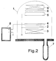
- Fig.2 shows the arrangement according to claim 6 of the invention formula, implementing the method according to claim 2 of the formula.
- Fig.3 shows the arrangement according to claim 7 of the formula which is used to implement the method of developing doped single-crystal carbon films according to claim 3 and 4 of the formula.
- the suggested arrangement (Fig.1) has a vacuum chamber 1 with annular anode 4 made of solid carbon, and cathode-target 2 made of solid carbon, under which there is magnet 3. It is additionally equipped with cathode 5 made of solid carbon, over which there is substrate 6 of single-crystal material. Cathodes 2 and 5 connected with each other and have negative potential with respect to anode 4, located between them.
- the vacuum chamber is equipped by the pumping system 7. Voltage between the anode and the cathode is supplied from a DC source.
- the arrangement shown in Fig.3, is additionally equipped with the doping unit, consisting of anode 12, cathode 13 made of doping material and magnet 14.
- the doping unit is connected with power source 15.
- Cathode 13 is located between anode 12 and magnet 14.
- the doping unit is arranged in such a way that there is a possibility to mix the ions of doping substance and carbon in the vicinity of substance 6.
- the suggested arrangement operates in the following way. With the help of the pumping out system 7, certain residual pressure is achieved, which value depends on the type of carbon film (graphite, diamond and etc.). Then the voltage is applied from the source 8 to anode 4 there is a possibility to get smouldering discharge between cathode 2 and anode 4.
- the distance between cathode and anode it is possible to get stable, structurally uniform carbon plasma which is sustained by means of carbon atoms and electrons, knocked out from the surface of cathode-target 2. In this case electrons, moving from cathode 2 towards anode 4, ionize carbon atoms.
- the arrangement is equipped with extra magnet 9, which form a magnetic field together with magnet 3.
- magnet 9 which form a magnetic field together with magnet 3.
- Fig.3 In order to get doped single-crystal films the arrangement (Fig.3) is used, where the spraying of cathode 13, made of doped material, is done simultaneously with the spraying of cathode 2 made of solid carbon.
- Cathode 13 doping is performed in a way similar to cathode 2 doping in the regime of smouldering discharge. This smouldering discharge is obtained by applying voltage from the source of DC 15.
- the flow of carbon plasma and that of a doping substance get mixed in the vicinity of substrate 6 and precipitate on it, form doped single-crystal carbon film.
- Example No 1 The process of developing single-crystal carbon film was carried out in vacuum chamber 1 under the pressure of 10 -4 Pa.
- the arrangement consisting of graphite cathode 2, annular graphite anode 4, substrate 6, made of single-crystal silicon wafer with orientation t (100), located behind the annular graphite cathode 5 and magnet 3, which is behind cathode 2 was used.
- Cathode 2 and cathode 4 are connected electrically with each other.
- Smouldering discharge was obtained from source 2 by applying voltage 5 kV between anode 4 and cathode 2 and 5. By choosing the distance between cathode 2 and 5 and anode 4, stable uniform carbon plasma of smouldering discharge was developed.
- the process of graphite cathode 2 doping in smouldering discharge and carbon ion precipitation on carbon substrate 6 resulted in single-crystal carbon film formation.
- the films are single-crystal and have the structure of a diamond with surface orientation (111).
- the films microhardness (according to Moos) is 1, which corresponds to diamond microhardness .
- example 2 the arrangement similar to the one described in example 1 was used. The difference was that the arrangement was equipped with additional magnet 9 to create the longitudinal magnetic field in the arrangement. This longitudinal magnetic field contribute to the density increase of the plasma, which made it possible to bring down voltage, sustaining 5 kV up and 3 kV at constant distances between cathode and anode. The results of the samples investigation showed, that the presence of additional magnet 9 did not have any obvious influence on the films single-crystallinity. Thus, in example 1, the growth rate was 100 ⁇ per hour while in example 2, growth rate increased up to 1000 ⁇ per hour with the rest of the parameters remaining constant.
- Example 3 Single-crystal doped film are developed in the arrangement similar to the one described in example 2 with the extra doping unit.
- the doping unit cathode was made of boron oxide.
- doping material boron
- By mixing the latter with the flow of carbon plasma and by precipitation of the mixed flow on silicon substrate, carbon films doped by boron, having the property of semiconductors of R-type, were obtained. Specific resistance of these semi-conductors was up ⁇ 10 4 Ohm m.
- the films produced in this way may be used in electronics, and in the jewelry industry, including X-ray structure investigation monochromators.
Landscapes
- Chemical & Material Sciences (AREA)
- Engineering & Computer Science (AREA)
- Materials Engineering (AREA)
- Metallurgy (AREA)
- Organic Chemistry (AREA)
- Chemical Kinetics & Catalysis (AREA)
- Mechanical Engineering (AREA)
- Crystallography & Structural Chemistry (AREA)
- Physics & Mathematics (AREA)
- Plasma & Fusion (AREA)
- Analytical Chemistry (AREA)
- Crystals, And After-Treatments Of Crystals (AREA)
Claims (7)
- Verfahren zum Herstellen einer einkristallinen Schicht aus Kohlenstoff in einer Vakuumkammer bei Restdruck, bei dem ein Kohlenstoffplasma durch Glimmentladung hergestellt wird zwischen einer Zerstäubungskathode (2) aus Homogenkohle und einer Ringanode (4) aus Homogenkohle, die zwischen der Zerstäubungskathode und einer zusätzlichen, eine Öffnung aufweisenden Kathode (5) aus Homogenkohle angeordnet ist, wobei die zusätzliche Kathode zwischen der Anode und einem Einkristallsubstrat (6) angeordnet ist, und bei dem Elektronen, die von der Oberfläche der Zerstäubungskathode gesprüht werden, durch Gleichstrom in einem Magnetsystem (3) gegen die Anode gelenkt werden, wodurch eine Kohlenstoffionenbeschleunigung aufgrund der Spannung zwischen der Ringanode und der zusätzlichen Kathode in einer solchen Weise erzeugt wird, daß Kohlenstoffionen auf dem Einkristallsubstrat abgeschieden werden.
- Verfahren nach Anspruch 1, bei dem zu dem Elektronenfeld zusätzlich ein longitudinales Magnetfeld aufgebracht wird.
- Verfahren nach Anspruch 1 oder 2, bei dem das Sprühen der Zerstäubungskathode aus Homogenkohle in Gegenwart einer Dotiermischung vorgenommen wird.
- Verfahren nach Anspruch 3, bei dem das Sprühen der Zerstäubungskathode aus Homogenkohle gleichzeitig mit dem Sprühen der Dotiermischung vorgenommen wird.
- Vorrichtung zum Herstellen einer einkristallinen Schicht aus Kohlenstoff mit einer Vakuumkammer, einem Magneten, einer Zerstäubungskathode aus Homogenkohle und einer Ringanode aus Homogenkohle und einem einkristallinen Substrat, dadurch gekennzeichnet, daß sie eine zusätzliche, eine Öffnung aufweisende Kathode aus Homogenkohle enthält, die zwischen der Anode und dem Substrat angeordnet ist, wobei der Magnet hinter der Zerstäubungskathode auf der von der Ringanode abgewandten Seite angeordnet ist.
- Vorrichtung nach Anspruch 5, die zusätzlich mit einem zusätzlichen Magneten ausgestattet ist, der über dem Substrat auf der von der zusätzlichen Kathode abgewandten Seite mit der Möglichkeit der Bildung eines longitudinalen Feldes angeordnet ist.
- Vorrichtung nach Anspruch 5 oder 6, die zusätzlich mit einer Dotiereinheit ausgestattet ist, die einen Magneten, eine Anode und eine Kathode aufweist, die aus Dotiermaterial hergestellt ist und zwischen der Anode und dem Magneten derart angeordnet ist, daß die Möglichkeit besteht, Ionenströme aus Dotiermaterial und Kohlenstoff zu mischen.
Applications Claiming Priority (3)
| Application Number | Priority Date | Filing Date | Title |
|---|---|---|---|
| KZ950100 | 1995-02-14 | ||
| KZ95010095 | 1995-02-14 | ||
| PCT/KZ1996/000001 WO1996025537A1 (en) | 1995-02-14 | 1996-02-12 | Method and apparatus for producing single crystal carbon films |
Publications (2)
| Publication Number | Publication Date |
|---|---|
| EP0809721A1 EP0809721A1 (de) | 1997-12-03 |
| EP0809721B1 true EP0809721B1 (de) | 1998-12-23 |
Family
ID=19720751
Family Applications (1)
| Application Number | Title | Priority Date | Filing Date |
|---|---|---|---|
| EP96902000A Expired - Lifetime EP0809721B1 (de) | 1995-02-14 | 1996-02-12 | Verfahren und vorrichtung zur herstellung von einkristallinen schichten aus kohlenstoff |
Country Status (3)
| Country | Link |
|---|---|
| EP (1) | EP0809721B1 (de) |
| DE (1) | DE69601216D1 (de) |
| WO (1) | WO1996025537A1 (de) |
Family Cites Families (3)
| Publication number | Priority date | Publication date | Assignee | Title |
|---|---|---|---|---|
| DE3712205A1 (de) * | 1987-04-10 | 1988-10-20 | Detlev Dipl Chem Dr Repenning | Verfahren zur herstellung von schichten mit hochharten diamantaehnlichen und/oder reibungsarmen eigenschaften |
| EP0360994B1 (de) * | 1988-09-20 | 1994-03-16 | International Business Machines Corporation | Vorrichtung und Verfahren zur Herstellung von Diamantfilmen bei tiefen Temperaturen |
| JPH06279185A (ja) * | 1993-03-25 | 1994-10-04 | Canon Inc | ダイヤモンド結晶およびダイヤモンド結晶膜の形成方法 |
-
1996
- 1996-02-12 WO PCT/KZ1996/000001 patent/WO1996025537A1/en not_active Ceased
- 1996-02-12 EP EP96902000A patent/EP0809721B1/de not_active Expired - Lifetime
- 1996-02-12 DE DE69601216T patent/DE69601216D1/de not_active Expired - Lifetime
Also Published As
| Publication number | Publication date |
|---|---|
| DE69601216D1 (de) | 1999-02-04 |
| WO1996025537A1 (en) | 1996-08-22 |
| EP0809721A1 (de) | 1997-12-03 |
Similar Documents
| Publication | Publication Date | Title |
|---|---|---|
| US3961103A (en) | Film deposition | |
| CA1308689C (en) | Method and apparatus for forming a thin film | |
| US6570172B2 (en) | Magnetron negative ion sputter source | |
| US4416755A (en) | Apparatus and method for producing semiconducting films | |
| US4376688A (en) | Method for producing semiconductor films | |
| US5039376A (en) | Method and apparatus for the plasma etching, substrate cleaning, or deposition of materials by D.C. glow discharge | |
| KR20040105606A (ko) | 이온원 장치 및 그의 클리닝 최적화 방법 | |
| US6388366B1 (en) | Carbon nitride cold cathode | |
| EP0203573B1 (de) | Mittels Elektronenstrahl angeregte Ionenstrahlquelle | |
| JP2556364B2 (ja) | 真空蒸着装置 | |
| JP3099819B2 (ja) | 半導体装置の製造方法 | |
| EP0809721B1 (de) | Verfahren und vorrichtung zur herstellung von einkristallinen schichten aus kohlenstoff | |
| JPH1187261A (ja) | 低ドーズ量のイオン注入方法及びその装置 | |
| JP2689419B2 (ja) | イオンドーピング装置 | |
| US20120000606A1 (en) | Plasma uniformity system and method | |
| JPS6380534A (ja) | プラズマ処理装置 | |
| JP3406769B2 (ja) | イオンプレーティング装置 | |
| JP2849831B2 (ja) | プラズマcvd装置 | |
| JP2977862B2 (ja) | プラズマ発生装置 | |
| JP3577785B2 (ja) | イオンビーム発生装置 | |
| GB2212520A (en) | Ion source | |
| JP2590502B2 (ja) | 不純物のドーピング方法 | |
| JPH0378954A (ja) | イオン源 | |
| JP2000306543A (ja) | イオン注入装置 | |
| JPH0798145B2 (ja) | プラズマ処理装置 |
Legal Events
| Date | Code | Title | Description |
|---|---|---|---|
| PUAI | Public reference made under article 153(3) epc to a published international application that has entered the european phase |
Free format text: ORIGINAL CODE: 0009012 |
|
| 17P | Request for examination filed |
Effective date: 19970904 |
|
| AK | Designated contracting states |
Kind code of ref document: A1 Designated state(s): DE FR GB |
|
| GRAG | Despatch of communication of intention to grant |
Free format text: ORIGINAL CODE: EPIDOS AGRA |
|
| 17Q | First examination report despatched |
Effective date: 19980309 |
|
| GRAG | Despatch of communication of intention to grant |
Free format text: ORIGINAL CODE: EPIDOS AGRA |
|
| GRAH | Despatch of communication of intention to grant a patent |
Free format text: ORIGINAL CODE: EPIDOS IGRA |
|
| GRAH | Despatch of communication of intention to grant a patent |
Free format text: ORIGINAL CODE: EPIDOS IGRA |
|
| GRAA | (expected) grant |
Free format text: ORIGINAL CODE: 0009210 |
|
| AK | Designated contracting states |
Kind code of ref document: B1 Designated state(s): DE FR GB |
|
| PG25 | Lapsed in a contracting state [announced via postgrant information from national office to epo] |
Ref country code: FR Free format text: LAPSE BECAUSE OF FAILURE TO SUBMIT A TRANSLATION OF THE DESCRIPTION OR TO PAY THE FEE WITHIN THE PRESCRIBED TIME-LIMIT Effective date: 19981223 |
|
| REF | Corresponds to: |
Ref document number: 69601216 Country of ref document: DE Date of ref document: 19990204 |
|
| PG25 | Lapsed in a contracting state [announced via postgrant information from national office to epo] |
Ref country code: DE Free format text: LAPSE BECAUSE OF FAILURE TO SUBMIT A TRANSLATION OF THE DESCRIPTION OR TO PAY THE FEE WITHIN THE PRESCRIBED TIME-LIMIT Effective date: 19990324 |
|
| EN | Fr: translation not filed | ||
| PLBE | No opposition filed within time limit |
Free format text: ORIGINAL CODE: 0009261 |
|
| STAA | Information on the status of an ep patent application or granted ep patent |
Free format text: STATUS: NO OPPOSITION FILED WITHIN TIME LIMIT |
|
| 26N | No opposition filed | ||
| PG25 | Lapsed in a contracting state [announced via postgrant information from national office to epo] |
Ref country code: GB Free format text: LAPSE BECAUSE OF NON-PAYMENT OF DUE FEES Effective date: 20000212 |
|
| GBPC | Gb: european patent ceased through non-payment of renewal fee |
Effective date: 20000212 |