EP0809301B1 - Integrierte Struktur mit reduziertem Injektionsstrom zwischen homologen Gebieten - Google Patents
Integrierte Struktur mit reduziertem Injektionsstrom zwischen homologen Gebieten Download PDFInfo
- Publication number
- EP0809301B1 EP0809301B1 EP96830277A EP96830277A EP0809301B1 EP 0809301 B1 EP0809301 B1 EP 0809301B1 EP 96830277 A EP96830277 A EP 96830277A EP 96830277 A EP96830277 A EP 96830277A EP 0809301 B1 EP0809301 B1 EP 0809301B1
- Authority
- EP
- European Patent Office
- Prior art keywords
- region
- transistor
- type
- current
- integrated structure
- Prior art date
- Legal status (The legal status is an assumption and is not a legal conclusion. Google has not performed a legal analysis and makes no representation as to the accuracy of the status listed.)
- Expired - Lifetime
Links
- 238000002347 injection Methods 0.000 title claims description 10
- 239000007924 injection Substances 0.000 title claims description 10
- 229910052751 metal Inorganic materials 0.000 claims description 18
- 239000002184 metal Substances 0.000 claims description 18
- 239000004065 semiconductor Substances 0.000 claims description 16
- 239000000463 material Substances 0.000 claims description 13
- 230000003134 recirculating effect Effects 0.000 claims description 5
- 230000005540 biological transmission Effects 0.000 claims description 3
- 230000001939 inductive effect Effects 0.000 claims description 2
- 239000004020 conductor Substances 0.000 claims 1
- 230000003071 parasitic effect Effects 0.000 description 40
- 239000000758 substrate Substances 0.000 description 14
- 239000000243 solution Substances 0.000 description 11
- 101100336279 Caenorhabditis elegans icl-1 gene Proteins 0.000 description 8
- 238000009413 insulation Methods 0.000 description 8
- 230000000694 effects Effects 0.000 description 7
- 230000010287 polarization Effects 0.000 description 6
- 230000002547 anomalous effect Effects 0.000 description 3
- 230000015572 biosynthetic process Effects 0.000 description 3
- 239000012535 impurity Substances 0.000 description 3
- 230000005684 electric field Effects 0.000 description 2
- 238000000034 method Methods 0.000 description 2
- 229920006395 saturated elastomer Polymers 0.000 description 2
- 230000004913 activation Effects 0.000 description 1
- 239000004411 aluminium Substances 0.000 description 1
- 229910052782 aluminium Inorganic materials 0.000 description 1
- XAGFODPZIPBFFR-UHFFFAOYSA-N aluminium Chemical compound [Al] XAGFODPZIPBFFR-UHFFFAOYSA-N 0.000 description 1
- 239000002699 waste material Substances 0.000 description 1
Images


Classifications
-
- H—ELECTRICITY
- H10—SEMICONDUCTOR DEVICES; ELECTRIC SOLID-STATE DEVICES NOT OTHERWISE PROVIDED FOR
- H10D—INORGANIC ELECTRIC SEMICONDUCTOR DEVICES
- H10D84/00—Integrated devices formed in or on semiconductor substrates that comprise only semiconducting layers, e.g. on Si wafers or on GaAs-on-Si wafers
- H10D84/60—Integrated devices formed in or on semiconductor substrates that comprise only semiconducting layers, e.g. on Si wafers or on GaAs-on-Si wafers characterised by the integration of at least one component covered by groups H10D10/00 or H10D18/00, e.g. integration of BJTs
- H10D84/641—Combinations of only vertical BJTs
- H10D84/643—Combinations of non-inverted vertical BJTs and inverted vertical BJTs
-
- H—ELECTRICITY
- H10—SEMICONDUCTOR DEVICES; ELECTRIC SOLID-STATE DEVICES NOT OTHERWISE PROVIDED FOR
- H10D—INORGANIC ELECTRIC SEMICONDUCTOR DEVICES
- H10D84/00—Integrated devices formed in or on semiconductor substrates that comprise only semiconducting layers, e.g. on Si wafers or on GaAs-on-Si wafers
- H10D84/60—Integrated devices formed in or on semiconductor substrates that comprise only semiconducting layers, e.g. on Si wafers or on GaAs-on-Si wafers characterised by the integration of at least one component covered by groups H10D10/00 or H10D18/00, e.g. integration of BJTs
- H10D84/63—Combinations of vertical and lateral BJTs
Definitions
- the present invention relates to integrated semiconductor structures and in particular, to an integrated structure according to the preamble to Claim 1.
- a widely used insulation technique consists of the creation within a "chip" of semiconductor material of insulation regions with the opposite type of conductivity to that of the semiconductor material. During the operation of these integrated structures, the semiconductor material of the chip is brought to a potential relative to the insulation regions, such that the P-N junctions created between the semiconductor material and the insulation regions are reverse biased; the reversed polarization of these junctions ensures the insulation between the regions in which the various components or circuit units are formed.
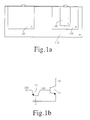
- the integrated structure shown in Figure la will be considered.
- P-type regions formed in an N-type semiconductor material naturally, corresponding considerations are applicable if the regions have the opposite doping.
- the integrated structure shown in the drawing comprises an N-type epitaxial layer 110 formed on a substrate, not shown in the drawing.
- Two P-type regions 120 and 130 are formed within the epitaxial layer 110; within the region 130 there is a further N-type region 140.
- the substrate, and hence the epitaxial layer 110 is kept at a positive potential relative to the potential of the regions 120 and 130; the P-N junctions created between the substrate 110 and the regions 120 and 130 therefore have reversed polarities, that is, polarities which ensure insulation between the two regions.
- a typical example is that in which the integrated structure described above is a mixed-type integrated circuit, that is, with insulated signal-processing circuits in one or more wells and with vertical power transistors having their collector (or drain) regions in the epitaxial layer 110. It is assumed that the region 120 constitutes the anode of a recirculating diode associated with a vertical power transistor, not shown, integrated in the same circuit and having an inductive load; the region 130, on the other hand, constitutes the insulation region of a well, the region 140, in which the signal-processing components of the control circuitry of the power transistor are integrated.
- the epitaxial layer 110 may be at a negative potential relative to that of the region 120, that is, the recirculation diode may be polarized for transmission.
- the two regions 120 and 130 form a parasitic component with the substrate, as shown schematically in the equivalent circuit shown in Figure 1b.
- the parasitic component T 1 is a lateral PNP transistor created by the P region 120 (emitter), by the N epitaxial layer 110 (base) and by the P region 130 (collector).
- a further parasitic component is constituted by a vertical NPN transistor Tv created by the N region 140 (collector), by the P region 130 (base) and by the N epitaxial layer 110 (emitter).
- the collector of the transistor T 1 is connected to the base of the transistor Tv (common region 130) and the emitter of the transistor Tv is connected to the base of the transistor T 1 (common epitaxial layer).
- the PNP transistor T 1 becomes conductive, causing an injection of current, the collector current of the transistor T 1 , from the region 120 to the region 130. In the example shown in the drawing, this injection of current also switches on the vertical parasitic NPN transistor Tv.
- the current gain and the base, collector and emitter currents, respectively, of a generic transistor Tn are indicated below by the symbols ⁇ n, Ibn, Icn and Ien.
- the current injected from the region 120 into the region 130, which is the collector current Icl of the transistor T 1 , is: Icl ⁇ l 1+ ⁇ l Iel
- This current Icl is equal to the current Ibv injected into the base of the transistor Tv.
- a first solution consists of suitable spacing of the two regions; however, this solution involves a considerable waste of useful area of the integrated structure.
- a different solution is that of increased doping of the base of the parasitic transistor, that is, the portion of the epitaxial layer disposed between the two P regions, by means of a suitable region with a high concentration of N-type impurities.
- the gain of the lateral parasitic PNP transistor is thus reduced; since, as shown above, the current injected into the P region 130 is proportional to the gain of this transistor, the injection of current is thus reduced.
- the substrate and hence the epitaxial layer 110
- this highly doped N-type region brings the upper surface of the chip to a potential close to that of the collector electrode of the power transistor.
- a further solution shown in Figures 2a, consists of the formation of a further P-type region 210 (a "channel stopper") in the epitaxial layer 110 disposed between the regions 120 and 130, that is, in the base region of the lateral parasitic transistor.
- This region 210 splits the parasitic component between the two regions 120 and 130 into two lateral parasitic transistors Tl1 and Tl2, as shown schematically in the equivalent circuit of Figure 2b.
- the lateral parasitic PNP transistor Tl1 is created by the P region 120 (emitter), by the N epitaxial layer 110 (base) and by the further P-type region 210 (collector), and the lateral parasitic PNP transistor Tl2 is created by the P-type region 210 (emitter), by the N epitaxial layer 110 (base) and by the region 130 (collector).
- the two transistors Tl1 and Tl2 have a common base (the epitaxial layer 110); moreover, the collector of the transistor Tl1 is connected to the emitter of the transistor Tl2 (common P-type region 210); as in the previous case, the collector of the transistor Tl2 is connected to the base of the transistor Tv (common P-type region 130) and the emitter of the transistor Tv is connected to the bases of the two transistors Tl1 and Tl2 (common epitaxial layer 110).
- one of the two parasitic transistors Tl1 and Tl2 is brought to a high level of saturation with a consequent reduction in its gain and hence in the injection of current into the region 130.
- FIG. 3a Another solution shown in Figure 3a, consists of the electrical connection of the P-type region 210 to the epitaxial layer 110 by means of a surface metal contact strip 310; in order to favour good ohmic contact with the surface of the epitaxial layer 110, in the example shown in the drawing there is also a region 320 with a high N-type concentration which prevents the formation of a PN junction between the N epitaxial layer 110 and the metal strip 310 (generally aluminium) containing P-type impurities.
- the emitter of the transistor Tl2 (P-type region 210) is short-circuited to its own base (the epitaxial layer 110) by means of the metal strip 310; the transistor Tl2 is therefore always cut off so that the injection of current between the two regions 120 and 130 is completely nullified.
- the substrate and therefore the epitaxial layer
- this solution also requires an adequate termination structure resulting in the occupation of a considerable area.
- a dynamic polarization circuit is used and is constituted by a vertical transistor of the same type as the parasitic transistor the switching-on of which is to be avoided.
- a further P-type region 410 is created in the epitaxial layer 110 and an N-type region 420 is formed therein.
- the N-type region 420 is connected electrically to the region 130 by means of a surface metal contact strip 430.
- circuit equivalent to the structure described above is shown in Figure 4b.
- the circuit shown in the drawing comprises the vertical parasitic NPN transistor Tv created by the N-type region 140 (collector), by the P-type region 130 (base) and by the N epitaxial layer 110 (emitter).
- the dynamic polarization circuit is constituted by a vertical NPN transistor Tp constituted by the N-type region 420 (collector), by the P-type region 410 (base) and by the N-type epitaxial layer 110 (emitter); as shown in the drawing, the emitter of the transistor Tp is connected to the emitter of the transistor Tv (common epitaxial layer 110) and the collector of the transistor Tp (N-type region 420) is connected to the base of the transistor Tv (region 130) by means of the metal connection 430.
- the circuit shown in the drawing comprises a further lateral parasitic transistor Tl', constituted by the P-type region 130 (collector) by the N-type epitaxial layer 110 (base) and by the P-type region 410 (emitter).
- the collector of the transistor Tl' is connected to the base of the transistor Tv (common region 130) and to the collector of the transistor Tp (by means of the metal connection 430), the emitter of the transistor Tl' is connected to the base of the transistor Tp (common P-type region 410), and the base of the transistor Tl is connected to the emitters of the transistors Tv and Tp (common epitaxial layer 110).
- the transistor Tp is supplied by the supply system of the integrated structure by means of suitable driving circuitry (not shown in the drawing). As soon as the substrate potential of the structure (that is, the potential of the epitaxial layer 110) falls below a predetermined threshold (higher than that necessary to make the vertical parasitic transistor Tv conductive) a driver stage constituted, for example, by a constant-current generator (not shown in the drawing) is activated and supplies to the base terminal of the transistor Tp a current of a value such as to bring the transistor to saturation. The base and the emitter of the transistor Tv are therefore kept at the same potential, thus preventing the vertical parasitic transistor from being switched on.
- suitable driving circuitry not shown in the drawing.
- the integrated structure is constituted by a mixed circuit (signal and power) comprising a vertical power transistor having its own collector included in the weakly doped N-type epitaxial layer 110 (the emitter is constituted by a region with strong N-type doping formed within a P-type region which constitutes the base of the same transistor).
- the transistor Tp is normally formed by the same process which is used for the formation of the power transistor described above; it is therefore constituted by an emitter region with a low level of doping (epitaxial layer 110) and by a collector region with a high level of doping (region 420) so that it has a very low current gain.
- the present invention provides a structure integrated in a chip of semiconductor material of a first type of conductivity, the integrated structure comprising a first region and a second region of a second type of conductivity, extending into the semiconductor material from a surface of the chip in order to form a first junction and a second junction, means for reducing the injection of current from the first region to the second region when the first junction is polarized for transmission, wherein the means include a third region of the second type of conductivity extending from the surface into a portion of the semiconductor material disposed between the first region and the second region, a fourth region of the first type of conductivity extending from the surface into the third region, and an electrical connection between the fourth region and the second region.
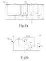
- the integrated structure 500 comprises, as described above, an N-type epitaxial layer 110 in which two P-type regions 120 and 130 are formed; in the region 130 there is a further N-type region 140.
- a further P-type region 510 is formed, inside which an N-type region 520 is formed.
- the N-type region 520 is connected electrically to the region 130, for example, by means of a surface metal contact strip 530.
- the circuit equivalent to the structure described above is shown in Figure 5b.
- the circuit shown in the drawing comprises a lateral parasitic PNP transistor Tl1' created by the P region 120 (emitter), by the N epitaxial layer 110 (base) and by the P-type region 510 (collector) and a lateral parasitic PNP transistor T12' created by the P-type region 510 (emitter), by the N epitaxial layer 110 (base) and by the region 130 (collector).
- the two transistors Tl1' and Tl2' have a common base (the epitaxial layer 110).
- the integrated structure according to the present invention comprises a vertical NPN transistor Tp' constituted by the N-type region 520 (collector), by the P-type region 510 (base) and by the N epitaxial layer 110 (emitter).
- the base of the transistor Tp' is connected to the collector of the transistor Tl1' and to the emitter of the transistor Tl2' (common P-type region 510) and the emitter of the transistor Tp' is connected to the bases of the transistors Tl1' and Tl2' (common epitaxial layer 110); moreover, the collectors of the two transistors Tp' and T12' are connected to one another by means of the metal connection 530.
- the integrated structure of the embodiment shown therefore comprises, as described above, the vertical parasitic NPN transistor Tv created by the N region 140 (collector), by the P region 130 (base and by the N epitaxial layer 110 (emitter).
- the base of the transistor Tv is connected to the collector of the transistor Tl2' (common region 130) and to the collector of the transistor Tp', by means of the metal connection 530;
- the emitter of the transistor Tv is connected to the bases of the transistors Tl1' and Tl2' and to the emitter of the transistor Tp' (common epitaxial layer 110).
- the current supplied by the transistor Tl1' is divided into a portion which is injected into the region 130 by means of the transistor Tl2' and a portion which serves to activate the transistor Tp'.
- the transistor Tp' enables all or some of the current injected by the transistor Tl2' into the region 130 to be extracted by means of its collector.
- the current thus extracted from the region 130 is sent to the epitaxial layer and hence to the substrate of the integrated structure by means of the emitter of the transistor Tp'.
- Ibp' k.Iel2'
- Icl1'-Iel2' k.Iel2'
- the transistor Tp' succeeds in causing a current greater than that injected by the transistor Tl2' to circulate, as it becomes saturated, it connects the base and the emitter of the parasitic transistor Tv to the same potential preventing it from being switched on; the structure described above therefore also acts as a dynamic insulation circuit between the region 130 and the substrate of the integrated structure.
- the integrated structure according to the present invention therefore offers a solution which can reduce (or even nullify) the injection of current between two homologous regions, at the same time preventing any vertical parasitic transistors from being switched on.
- the integrated structure according to the present invention does not require a driver stage and, in particular, does not require a constant-current generator to supply the current to the base terminal of the transistor Tp'; in fact, for this purpose it uses the current which is injected from one P-type region to the other, thus reducing the power absorbed from the supply of the integrated structure.
- dedicated driving circuitry which anticipates the switching-on of the transistor Tp', fixing its switching threshold at a level below that achieved automatically by the circuit described above.
- the current supplied to the base terminal of the transistor Tp' depends upon the size of the negative voltage difference between the substrate (and hence the epitaxial layer 110) and the P-type regions. Since the current which is injected by the region 120 into the region 130 and which the transistor Tp' has to extract also depends on the same voltage difference, the integrated structure according to the present invention clearly forms a system in which the base current of the transistor Tp' is auto-adaptive.
- the region 120 is connected to a reference terminal (earth); a typical example is that of a mixed integrated circuit (signal and power) in which the region 120 is the anode of a recirculating diode associated with a power transistor.
- a reference terminal earth
- a typical example is that of a mixed integrated circuit (signal and power) in which the region 120 is the anode of a recirculating diode associated with a power transistor.
- the channels formed between the P-type region 510 and the P-type regions 120 and 130 can retain limited dimensions so that, if the substrate (and hence the epitaxial layer 110) has to withstand high voltages (as in the mixed integrated circuit described above), the field lines generated by this voltage do not succeed in reaching the upper surface of the chip; the integrated structure according to the present invention does not therefore need termination devices with a consequent saving in chip area.
- a further advantage of the structure according to the present invention is that the current is extracted from the region 130 close to the region into which it is injected from the region 120. The path of the current is thus reduced, preventing consequent voltage drops, particularly along the metal strip 530 which connects the region 130 to the vertical transistor Tp'.
- This advantage is particularly important in the case of a mixed integrated circuit in which the P-type region 130 is the region insulating a well in which the signal-processing components of the control circuitry are integrated; in fact, in this case, it would be necessary to have a fairly dense network of surface metal contact strips connecting a fairly extensive region in the narrow regions available between the various signal components.
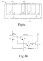
- the integrated structure 600 comprises, as described above, an N-type epitaxial layer 110, in which two P-type regions 120 and 130 are formed; a further N-type region 140 is present within the region 130.
- the region 120 comprises an N-type region 610 electrically connected to the region 120 by means of a surface metal contact strip 620.
- the P-type region which, in the embodiment of Figure 5a, defines the base region of the transistor Tp' (the P region 510 in which the N region 520 is formed) is joined to the P region 120; in practice, a further N-type region 630 (corresponding to the N region 520 of Figure 5a) is formed in the region 120 and is connected electrically to the region 130 by means of a further surface metal contact strip 640 (corresponding to the metal strip 530 of Figure 5a).
- the circuit equivalent to the structure described above is shown in Figure 6b.
- the circuit shown in the drawing comprises, as described above, the lateral parasitic PNP transistor Tl created by the P-type region 120 (emitter), by the N epitaxial layer 110 (base), and by the P-type region 130 (collector) and the vertical parasitic NPN transistor Tv created by the N region 140 (collector), by the P-type region 130 (base) and by the N epitaxial layer 110 (emitter).
- the collector of the transistor T1 is connected to the base of the transistor Tv (common region 130) and the emitter of the transistor Tv is connected to the base of the transistor Tl (common epitaxial layer 110).
- the integrated structure of Figure 6a comprises a vertical NPN transistor Td constituted by the N-type region 610 (collector), by the P-type region 120 (base), and by the N epitaxial layer 110 (emitter).
- the emitter of the transistor Td is connected to the base of the transistor Tl and to the emitter of the transistor Tv (common epitaxial layer 110); the base of the transistor Td is also short-circuited to its own collector by means of the metal strip 620.
- the transistor Td therefore forms a diode of which the anode is constituted by the base terminal and the cathode by the emitter terminal.
- This structure is typically used in a mixed integrated circuit (signal and power) in which the base-emitter diode constituted by the transistor Td has its anode connected to the earth terminal and constitutes a recirculating diode for a power transistor.
- the integrated structure of the present embodiment of the invention comprises a vertical NPN transistor Tp'' constituted by the N-type region 630 (collector), by the P-type region 120 (base) and by the N epitaxial layer 110 (emitter).
- This solution therefore provides for the transistor Tp'' which has the same function as the transistor Tp' of the structure of Figure 5a, to be integrated within the same region 120.
- the base of the transistor Tp'' is connected to the base of the transistor Td and to the emitter of the transistor Tl (common region 120) and the emitter of the transistor Tp'' is connected to the base of the transistor Tl and to the emitters of the transistors Td and Tv (common epitaxial layer 110); moreover, the collectors of the two transistors Tp'' and Tl are connected to one another by the metal connection 640.
- the two transistors Td and Tp'' define a current mirror so that the collector current of the transistor Tp'' is proportional to the current entering through the metal strip 620 of the transistor Td (less the portion injected into the region 130 by the lateral parasitic transistor Tl); this current mirror thus provides the necessary current to the base terminal of the transistor Tp'' making use of the current circulating in the diode constituted by the transistor Td.
- the integrated structure described offers all of the advantages of the structure described previously.
- the current which is injected from the region 120 into the region 130 and which the transistor Tp'' has to extract depends upon the size of the negative voltage difference between the substrate (and hence the epitaxial layer 110) and the region 120. The same dependency applies to the current circulating in the diode constituted by the transistor Td and, with reference to the foregoing, also in the transistor Tp''.
Landscapes
- Bipolar Integrated Circuits (AREA)
- Bipolar Transistors (AREA)
Claims (6)
- Eine Struktur, die in einen Chip (500) aus einem Halbleitermaterial (110) eines ersten Leitfähigkeitstyps integriert ist, wobei die integrierte Struktur folgende Merkmale aufweist:eine erste Region (120) und eine zweite Region (130) eines zweiten Leitfähigkeitstyps, die sich von einer Oberfläche des Chips (500) in das Halbleitermaterial (110) erstrecken, um einen ersten Übergang (120-110) und einen zweiten Übergang (130-110) zu bilden,eine Einrichtung zum Reduzieren des Injektionsstroms von der ersten Region (120) zu der zweiten Region (130), wenn der erste Übergang für eine Übertragung polarisiert ist,wobei die Einrichtung eine dritte Region (510) des zweiten Leitfähigkeitstyps aufweist, die sich von der Oberfläche in einen Abschnitt des Halbleitermaterials (110) erstreckt, der zwischen der ersten Region (120) und der zweiten Region (130) angeordnet ist, gekennzeichnet durcheine vierte Region (520) des ersten Leitfähigkeitstyps, die sich von der Oberfläche in die dritte Region (510) erstreckt, undeine elektrische Verbindung (530) zwischen der vierten Region (520) und der zweiten Region (130).
- Eine integrierte Struktur nach Anspruch 1, bei der die elektrische Verbindung (530) einen Metalleiter in einem ohmschen Oberflächenkontakt mit der vierten Region (520) und der zweiten Region (130) aufweist.
- Eine integrierte Struktur (500) nach Anspruch 1 oder 2, die ferner eine fünfte Region (140) des ersten Leitfähigkeitstyps aufweist, die sich von der Oberfläche in die zweite Region (130) erstreckt.
- Eine integrierte Struktur nach einem beliebigen der Ansprüche 1 bis 3, bei der die dritte Region mit der ersten Region (120) verschmolzen ist, wobei die integrierte Struktur eine sechste Region (610) des ersten Leitfähigkeitstyps, die sich von der Oberfläche in die erste Region (120) erstreckt, und eine elektrische Oberflächenverbindungseinrichtung (620) zwischen der sechsten Region (610) und der ersten Region (120) aufweist.
- Eine integrierte Struktur nach einem beliebigen der Ansprüche 1 bis 4, die ferner einen Leistungstransistor zum Steuern einer induktiven Last aufweist, dessen Kollektorregion in dem Halbleitermaterial (110) angeordnet ist, wobei der erste Übergang (120-110) eine Rückführungsdiode, die dem Leistungstransistor zugeordnet ist, bildet.
- Eine integrierte Struktur gemäß einem beliebigen der vorhergehenden Ansprüche, bei der der erste Leitfähigkeitstyp der N-Typ und der zweite Leitfähigkeitstyp der P-Typ ist.
Priority Applications (4)
| Application Number | Priority Date | Filing Date | Title |
|---|---|---|---|
| EP96830277A EP0809301B1 (de) | 1996-05-14 | 1996-05-14 | Integrierte Struktur mit reduziertem Injektionsstrom zwischen homologen Gebieten |
| DE69609053T DE69609053T2 (de) | 1996-05-14 | 1996-05-14 | Integrierte Struktur mit reduziertem Injektionsstrom zwischen homologen Gebieten |
| JP9139235A JPH1056074A (ja) | 1996-05-14 | 1997-05-13 | 同質部分間の電流注入を減少させる集積構造 |
| US08/855,212 US6060762A (en) | 1996-05-14 | 1997-05-13 | Integrated structure with reduced injection of current between homologous regions |
Applications Claiming Priority (1)
| Application Number | Priority Date | Filing Date | Title |
|---|---|---|---|
| EP96830277A EP0809301B1 (de) | 1996-05-14 | 1996-05-14 | Integrierte Struktur mit reduziertem Injektionsstrom zwischen homologen Gebieten |
Publications (2)
| Publication Number | Publication Date |
|---|---|
| EP0809301A1 EP0809301A1 (de) | 1997-11-26 |
| EP0809301B1 true EP0809301B1 (de) | 2000-06-28 |
Family
ID=8225908
Family Applications (1)
| Application Number | Title | Priority Date | Filing Date |
|---|---|---|---|
| EP96830277A Expired - Lifetime EP0809301B1 (de) | 1996-05-14 | 1996-05-14 | Integrierte Struktur mit reduziertem Injektionsstrom zwischen homologen Gebieten |
Country Status (4)
| Country | Link |
|---|---|
| US (1) | US6060762A (de) |
| EP (1) | EP0809301B1 (de) |
| JP (1) | JPH1056074A (de) |
| DE (1) | DE69609053T2 (de) |
Family Cites Families (5)
| Publication number | Priority date | Publication date | Assignee | Title |
|---|---|---|---|---|
| JPS61268036A (ja) * | 1985-05-23 | 1986-11-27 | Toshiba Corp | 半導体装置 |
| JPS62136872A (ja) * | 1985-12-11 | 1987-06-19 | Oki Electric Ind Co Ltd | バイポ−ラ型半導体集積回路装置の製造方法 |
| DE58907969D1 (de) * | 1988-02-15 | 1994-08-04 | Siemens Ag | Schaltungsanordnung zum Schutze einer integrierten Schaltung. |
| US5287047A (en) * | 1991-03-15 | 1994-02-15 | Rohm Co., Ltd. | Motor drive circuit and motor drive system using the same |
| US5514901A (en) * | 1994-05-17 | 1996-05-07 | Allegro Microsystems, Inc. | Epitaxial island with adjacent asymmetrical structure to reduce collection of injected current from the island into other islands |
-
1996
- 1996-05-14 DE DE69609053T patent/DE69609053T2/de not_active Expired - Fee Related
- 1996-05-14 EP EP96830277A patent/EP0809301B1/de not_active Expired - Lifetime
-
1997
- 1997-05-13 US US08/855,212 patent/US6060762A/en not_active Expired - Lifetime
- 1997-05-13 JP JP9139235A patent/JPH1056074A/ja active Pending
Also Published As
| Publication number | Publication date |
|---|---|
| JPH1056074A (ja) | 1998-02-24 |
| US6060762A (en) | 2000-05-09 |
| DE69609053T2 (de) | 2001-03-29 |
| DE69609053D1 (de) | 2000-08-03 |
| EP0809301A1 (de) | 1997-11-26 |
Similar Documents
| Publication | Publication Date | Title |
|---|---|---|
| US5914522A (en) | Power semiconductor structure with lateral transistor driven by vertical transistor | |
| US5883413A (en) | Lateral high-voltage DMOS transistor with drain zone charge draining | |
| US4131908A (en) | Semiconductor protection device having a bipolar lateral transistor | |
| KR890004472B1 (ko) | Cmos 집적회호 | |
| US4117507A (en) | Diode formed in integrated-circuit structure | |
| US5559348A (en) | Semiconductor device having insulated gate bipolar transistor | |
| US20020053717A1 (en) | Semiconductor apparatus | |
| US6365940B1 (en) | High voltage trigger remote-cathode SCR | |
| US4491746A (en) | Self-substrate-bias circuit device | |
| JPH0793383B2 (ja) | 半導体装置 | |
| US20010040266A1 (en) | Integrated circuit with highly efficient junction insulation | |
| US4622573A (en) | CMOS contacting structure having degeneratively doped regions for the prevention of latch-up | |
| EP0113334A2 (de) | Im Normalstand abgeschaltete Halbleiteranordnung mit niedrigem Betriebswiderstand und analoge Schaltung | |
| KR100286842B1 (ko) | 역전압 보호 회로를 구비한 파워 디바이스 | |
| JPH10173128A (ja) | 接合が絶縁された集積回路の寄生効果を抑制する方法および装置 | |
| JPH06188372A (ja) | 集積半導体回路 | |
| US4942440A (en) | High voltage semiconductor devices with reduced on-resistance | |
| US6525392B1 (en) | Semiconductor power device with insulated circuit | |
| EP0084000A2 (de) | CMOS Anordnung | |
| US6060762A (en) | Integrated structure with reduced injection of current between homologous regions | |
| US6441445B1 (en) | Integrated device with bipolar transistor and electronic switch in “emitter switching” configuration | |
| JPH1117198A (ja) | 集積mosパワー・トランジスタを含むコンポーネントのロジック・ウエルの保護 | |
| KR0138917B1 (ko) | 반도체 소자 | |
| CA1289267C (en) | Latchup and electrostatic discharge protection structure | |
| US5751052A (en) | Inductive driver circuit and method therefor |
Legal Events
| Date | Code | Title | Description |
|---|---|---|---|
| PUAI | Public reference made under article 153(3) epc to a published international application that has entered the european phase |
Free format text: ORIGINAL CODE: 0009012 |
|
| 17P | Request for examination filed |
Effective date: 19970227 |
|
| AK | Designated contracting states |
Kind code of ref document: A1 Designated state(s): DE FR GB IT |
|
| GRAG | Despatch of communication of intention to grant |
Free format text: ORIGINAL CODE: EPIDOS AGRA |
|
| GRAG | Despatch of communication of intention to grant |
Free format text: ORIGINAL CODE: EPIDOS AGRA |
|
| GRAH | Despatch of communication of intention to grant a patent |
Free format text: ORIGINAL CODE: EPIDOS IGRA |
|
| 17Q | First examination report despatched |
Effective date: 19990303 |
|
| GRAH | Despatch of communication of intention to grant a patent |
Free format text: ORIGINAL CODE: EPIDOS IGRA |
|
| GRAA | (expected) grant |
Free format text: ORIGINAL CODE: 0009210 |
|
| AK | Designated contracting states |
Kind code of ref document: B1 Designated state(s): DE FR GB IT |
|
| REF | Corresponds to: |
Ref document number: 69609053 Country of ref document: DE Date of ref document: 20000803 |
|
| ITF | It: translation for a ep patent filed | ||
| ET | Fr: translation filed | ||
| PLBE | No opposition filed within time limit |
Free format text: ORIGINAL CODE: 0009261 |
|
| STAA | Information on the status of an ep patent application or granted ep patent |
Free format text: STATUS: NO OPPOSITION FILED WITHIN TIME LIMIT |
|
| 26N | No opposition filed | ||
| REG | Reference to a national code |
Ref country code: GB Ref legal event code: IF02 |
|
| PGFP | Annual fee paid to national office [announced via postgrant information from national office to epo] |
Ref country code: DE Payment date: 20040527 Year of fee payment: 9 |
|
| PG25 | Lapsed in a contracting state [announced via postgrant information from national office to epo] |
Ref country code: IT Free format text: LAPSE BECAUSE OF NON-PAYMENT OF DUE FEES;WARNING: LAPSES OF ITALIAN PATENTS WITH EFFECTIVE DATE BEFORE 2007 MAY HAVE OCCURRED AT ANY TIME BEFORE 2007. THE CORRECT EFFECTIVE DATE MAY BE DIFFERENT FROM THE ONE RECORDED. Effective date: 20050514 |
|
| PG25 | Lapsed in a contracting state [announced via postgrant information from national office to epo] |
Ref country code: DE Free format text: LAPSE BECAUSE OF NON-PAYMENT OF DUE FEES Effective date: 20051201 |
|
| PGFP | Annual fee paid to national office [announced via postgrant information from national office to epo] |
Ref country code: GB Payment date: 20070427 Year of fee payment: 12 |
|
| PGFP | Annual fee paid to national office [announced via postgrant information from national office to epo] |
Ref country code: FR Payment date: 20070529 Year of fee payment: 12 |
|
| GBPC | Gb: european patent ceased through non-payment of renewal fee |
Effective date: 20080514 |
|
| REG | Reference to a national code |
Ref country code: FR Ref legal event code: ST Effective date: 20090119 |
|
| PG25 | Lapsed in a contracting state [announced via postgrant information from national office to epo] |
Ref country code: FR Free format text: LAPSE BECAUSE OF NON-PAYMENT OF DUE FEES Effective date: 20080602 |
|
| PG25 | Lapsed in a contracting state [announced via postgrant information from national office to epo] |
Ref country code: GB Free format text: LAPSE BECAUSE OF NON-PAYMENT OF DUE FEES Effective date: 20080514 |