EP0809131A2 - Plasmaadressierte Flüssigkristallanzeige mit verringerter Kapazität der Datenelektrode - Google Patents
Plasmaadressierte Flüssigkristallanzeige mit verringerter Kapazität der Datenelektrode Download PDFInfo
- Publication number
- EP0809131A2 EP0809131A2 EP97303379A EP97303379A EP0809131A2 EP 0809131 A2 EP0809131 A2 EP 0809131A2 EP 97303379 A EP97303379 A EP 97303379A EP 97303379 A EP97303379 A EP 97303379A EP 0809131 A2 EP0809131 A2 EP 0809131A2
- Authority
- EP
- European Patent Office
- Prior art keywords
- upper substrate
- separating layer
- data drive
- display panel
- layer
- Prior art date
- Legal status (The legal status is an assumption and is not a legal conclusion. Google has not performed a legal analysis and makes no representation as to the accuracy of the status listed.)
- Ceased
Links
Images

Classifications
-
- G—PHYSICS
- G02—OPTICS
- G02F—OPTICAL DEVICES OR ARRANGEMENTS FOR THE CONTROL OF LIGHT BY MODIFICATION OF THE OPTICAL PROPERTIES OF THE MEDIA OF THE ELEMENTS INVOLVED THEREIN; NON-LINEAR OPTICS; FREQUENCY-CHANGING OF LIGHT; OPTICAL LOGIC ELEMENTS; OPTICAL ANALOGUE/DIGITAL CONVERTERS
- G02F1/00—Devices or arrangements for the control of the intensity, colour, phase, polarisation or direction of light arriving from an independent light source, e.g. switching, gating or modulating; Non-linear optics
- G02F1/01—Devices or arrangements for the control of the intensity, colour, phase, polarisation or direction of light arriving from an independent light source, e.g. switching, gating or modulating; Non-linear optics for the control of the intensity, phase, polarisation or colour
- G02F1/13—Devices or arrangements for the control of the intensity, colour, phase, polarisation or direction of light arriving from an independent light source, e.g. switching, gating or modulating; Non-linear optics for the control of the intensity, phase, polarisation or colour based on liquid crystals, e.g. single liquid crystal display cells
- G02F1/133—Constructional arrangements; Operation of liquid crystal cells; Circuit arrangements
- G02F1/1333—Constructional arrangements; Manufacturing methods
- G02F1/13334—Plasma addressed liquid crystal cells [PALC]
Definitions
- This invention relates to a plasma addressed liquid crystal display panel with reduced data drive electrode capacitance.
- U.S. Patent 5,077,553 discloses apparatus for addressing data storage elements. A practical implementation of the apparatus shown in U.S. Patent 5,077,553 is illustrated schematically in FIGS. 4-6 of the accompanying drawings.
- the display panel shown in FIGS. 4-6 comprises, in sequence from below, a polarizer 2, a channel substrate 4, a cover sheet 6 (commonly known as a microsheet) having a thickness of about 50 ⁇ m, a layer 10 of electro-optic material having a thickness of about 5 ⁇ m, an array of parallel transparent data drive electrodes 12 at uniform width and spacing, an upper substrate 14 carrying the data drive electrodes, and an upper polarizer 16.
- the distance across the gap between two adjacent data drive electrodes is typically in the range from 50 ⁇ m to 200 ⁇ m.
- the channel substrate 2 is typically made of glass and is formed with multiple parallel channels 20 in its upper main face.
- the channels 20 are filled with an ionizable gas, such as helium.
- a ground electrode and a strobe electrode are provided in each of the channels 20.
- the channels 20 are orthogonal to the data drive electrodes 12 and the region where a data drive electrode crosses a channel (when viewed perpendicularly to the panel) forms a discrete panel element 22.
- Each panel element can be considered to include elements of the layer 10 and the upper and lower polarizers 2 and 16.
- the panel elements include color filters (not shown) between the layer 10 and the upper substrate 14.
- Adjacent panel elements 22 are spaced apart along a data drive electrode 12 and/or a channel 20, as shown in FIG. 6.
- the region of the upper surface of the display panel that bounds the panel element constitutes a single pixel 24 of the display panel.
- the upper polarizer In the event that a pixel is off, the upper polarizer passes light received from the volume element of electro-optic material and the pixel is illuminated, whereas if a pixel is on, the upper polarizer blocks light received from the volume element of electro-optic material and the pixel is not illuminated.
- Black surround material (not shown) is provided between adjacent panel elements in order to absorb stray light.
- a finite time elapses before the data drive electrode reaches the desired potential.
- the length of time depends on the resistivity of the data drive electrode and on the capacitance between the data drive electrode and conductive elements that are in the vicinity of the data drive electrode.
- a plasma addressed liquid crystal display panel In order to avoid objectionable flicker, it is necessary to refresh the image displayed by a plasma addressed liquid crystal display panel at a rate of at least about 60 Hz.
- the number of lines of data that can be displayed in a field at a refresh rate of 60 Hz depends in part on the time taken to change the potential of a data drive electrode.
- the capacitance between two thin, coplanar strip-form conductors that are of uniform width and spacing and are disposed between two dielectric media is proportional to the sum of the dielectric constants of the two dielectric media. Accordingly, the capacitance between two adjacent drive electrodes of a plasma addressed liquid crystal display panel having the configuration shown in FIGS. 4-6 is approximately proportional to the sum of the dielectric constant of the medium above the data drive electrodes, i.e. the glass of the upper substrate, and the dielectric constant of the medium below the data drive electrodes.
- the dielectric constant of glass that is suitable to form the upper substrate is typically in the range from about 3 to 10.
- a plasma addressed liquid crystal display panel comprising a layer of electro-optic material, an upper substrate having a lower surface that confronts the layer of electro-optic material and also having an upper surface, a separating layer between the lower surface of the upper substrate and the layer of electro-optic material, and an array of data drive electrodes attached to the separating layer and disposed between the separating layer and the layer of electro-optic material, whereby the separating layer is interposed between the data drive electrodes and the upper substrate, and wherein the separating layer is made of a material having a lower dielectric constant than the material of the upper substrate.
- an upper substrate assembly for a plasma addressed liquid crystal display panel comprising a layer of electro-optic material, an upper substrate having a lower surface that confronts the layer of electro-optic material and also having an upper surface, a separating layer between the lower surface of the upper substrate and the layer of electro-optic material, and an array of data drive electrodes attached to the separating layer and disposed between the separating layer and the layer of electro-optic material, whereby the separating layer is interposed between the data drive electrodes and the upper substrate, and wherein the separating layer is made of a material having a lower dielectric constant than the material of the upper substrate.
- the capacitance between two adjacent coplanar strip-form conductors of uniform width and spacing depends on the sum of the dielectric constants of the two media at opposite respective sides of the plane of the conductors.
- the capacitance between the conductors depends more strongly on the dielectric constant of that medium at a distance from the plane of the conductors that is less than the distance across the gap between the conductors than on the dielectric constant of the medium at a distance from the plane of the conductors that is substantially greater than the distance across the gap.
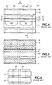
- the plasma display panel shown in FIG. 1 differs from that described with reference to FIGS. 4-6 by virtue of there being a separating layer 30 between the upper substrate 14 and the data drive electrodes 12.
- the thickness of the separating layer 30 is approximately equal to the distance g across the gap between the data drive electrodes. Accordingly, the capacitance between the data drive electrodes is substantially independent of the dielectric constant of the glass of the upper substrate 14 and is substantially proportional to the sum of the dielectric constant of the material of the separating layer and the dielectric constant of the medium beneath the data drive electrodes.
- the separating layer 30 is made of a material having a lower dielectric constant than the glass of the upper substrate. Therefore, the capacitance between the data drive electrodes of the panel shown in FIG. 1 is less than that for a plasma display panel that is of the same construction except that it does not include the separating layer 30. Because of the reduction in capacitance, the power required to drive the display panel shown in FIG. 1 is less than that required to drive a display panel of the same construction except for the separating layer.
- a suitable material for the separating layer 30 is the thermosetting resin known as benzocyclobutene, which has a dielectric constant of about 2.7 at 10 kHz and is commercially available from Dow Chemical Company.
- benzocyclobutene is applied to the upper substrate by spinning it on to the lower surface of the upper substrate and heating it so that it polymerizes.
- the data drive electrodes are formed on the lower surface of the separating layer, and color filters and black surround material are deposited partially on the data drive electrodes and partially on the separating layer.
- the data drive electrodes 12 are not deposited on the upper substrate 14 but are deposited on a thin sheet 32 of a transparent material and the sheet 32 is held in parallel spaced relationship with respect to the lower surface of the upper substrate by spacers 36.
- the spacers 36 which are illustrated in FIGS. 2 and 3 as being cylindrical in configuration, are located outside the panel elements 22 so that they do not occlude the panel elements.
- the spacers may be made of benzocyclobutene and may be formed by spinning benzocyclobutene on to the lower surface of the upper substrate 14 to form a layer of uniform thickness, heating the layer of benzocyclobutene in order to polymerize it, and selectively removing the layer using conventional photolithographic processes.
- the assembly of the sheet 32 and the data drive electrodes 12 attached thereto is attached to the spacers 36 projecting from the lower surface of the upper substrate using a suitable adhesive, such as an epoxy adhesive. It may be desired to seal the space between the sheet 32 and the upper substrate around the periphery of the upper substrate in order to allow partial evacuation of this space.
- the distance between the data drive electrodes and the lower surface of the upper substrate is greater than the distance across the gap between the data drive electrodes and so the capacitance between two adjacent data drive electrodes is substantially independent of the dielectric constant of the glass of the upper substrate.
- the dielectric constant of the material of the sheet 32 makes only a small contribution to the capacitance between two adjacent data drive electrodes. Nevertheless, because the electric field between the data drive electrodes is larger in the sheet 32 than in the space between the sheet 32 and the upper substrate, it is desirable that the sheet 32 be made of low dielectric constant material, such as a synthetic polymer material.
- the dielectric constant of the medium between the sheet 32 and the upper substrate 14 is not uniform, because of the presence of the spacers 36, but it is in any event substantially less than that of glass.
- the combined effect of the sheet 32 and the dielectric medium between the sheet 32 and the upper substrate is to reduce the effective dielectric constant of the medium above the data drive electrodes so that it is substantially lower than that of the glass of the upper substrate. In this manner, the capacitance between the data drive electrodes is substantially reduced relative to the conventional display panel shown in FIGS. 4-6.
Landscapes
- Physics & Mathematics (AREA)
- Nonlinear Science (AREA)
- Mathematical Physics (AREA)
- Plasma & Fusion (AREA)
- Chemical & Material Sciences (AREA)
- Crystallography & Structural Chemistry (AREA)
- Engineering & Computer Science (AREA)
- General Physics & Mathematics (AREA)
- Optics & Photonics (AREA)
- Liquid Crystal (AREA)
- Devices For Indicating Variable Information By Combining Individual Elements (AREA)
- Gas-Filled Discharge Tubes (AREA)
- Liquid Crystal Display Device Control (AREA)
- Control Of Indicators Other Than Cathode Ray Tubes (AREA)
Applications Claiming Priority (2)
| Application Number | Priority Date | Filing Date | Title |
|---|---|---|---|
| US1822996P | 1996-05-24 | 1996-05-24 | |
| US18229P | 1996-05-24 |
Publications (2)
| Publication Number | Publication Date |
|---|---|
| EP0809131A2 true EP0809131A2 (de) | 1997-11-26 |
| EP0809131A3 EP0809131A3 (de) | 1998-03-04 |
Family
ID=21786884
Family Applications (1)
| Application Number | Title | Priority Date | Filing Date |
|---|---|---|---|
| EP97303379A Ceased EP0809131A3 (de) | 1996-05-24 | 1997-05-19 | Plasmaadressierte Flüssigkristallanzeige mit verringerter Kapazität der Datenelektrode |
Country Status (6)
| Country | Link |
|---|---|
| US (1) | US5909260A (de) |
| EP (1) | EP0809131A3 (de) |
| JP (1) | JP3243602B2 (de) |
| KR (1) | KR970077014A (de) |
| CN (1) | CN1180880A (de) |
| TW (1) | TW346617B (de) |
Families Citing this family (6)
| Publication number | Priority date | Publication date | Assignee | Title |
|---|---|---|---|---|
| US6226056B1 (en) * | 1997-07-28 | 2001-05-01 | Sharp Kabushiki Kaisha | Plasma addressed liquid crystal display device having conductor through dielectric sheet attached to conductive layer centrally located in discharge channel |
| JPH11295706A (ja) * | 1998-04-15 | 1999-10-29 | Sony Corp | プラズマアドレス液晶表示装置 |
| US6849935B2 (en) | 2002-05-10 | 2005-02-01 | Sarnoff Corporation | Low-cost circuit board materials and processes for area array electrical interconnections over a large area between a device and the circuit board |
| USRE41914E1 (en) | 2002-05-10 | 2010-11-09 | Ponnusamy Palanisamy | Thermal management in electronic displays |
| CN1313870C (zh) * | 2003-05-09 | 2007-05-02 | 统宝光电股份有限公司 | 彩色滤光片及其制作方法 |
| WO2007105296A1 (ja) | 2006-03-13 | 2007-09-20 | Kabushiki Kaisha Shofu | アシルフォスフィンオキサイド基を有するカンファーキノン誘導体、それを含有する光重合触媒および光・化学重合触媒ならびにそれらを含有する硬化性組成物 |
Family Cites Families (6)
| Publication number | Priority date | Publication date | Assignee | Title |
|---|---|---|---|---|
| JPH03103830A (ja) * | 1989-09-19 | 1991-04-30 | Toppan Printing Co Ltd | アクティブマトリクス型液晶表示装置 |
| JP2847666B2 (ja) * | 1993-03-04 | 1999-01-20 | テクトロニクス・インコーポレイテッド | 電気光学表示方法 |
| JPH0743692A (ja) * | 1993-07-27 | 1995-02-14 | Sony Corp | プラズマアドレス液晶表示装置 |
| JP3329109B2 (ja) * | 1994-12-02 | 2002-09-30 | ソニー株式会社 | プラズマアドレス表示装置 |
| US5835167A (en) * | 1994-12-21 | 1998-11-10 | Philips Electronics North America | Plasma addressed liquid crystal display with reduced column voltages |
| US5641974A (en) * | 1995-06-06 | 1997-06-24 | Ois Optical Imaging Systems, Inc. | LCD with bus lines overlapped by pixel electrodes and photo-imageable insulating layer therebetween |
-
1997
- 1997-05-16 US US08/857,473 patent/US5909260A/en not_active Expired - Fee Related
- 1997-05-19 EP EP97303379A patent/EP0809131A3/de not_active Ceased
- 1997-05-20 TW TW086106751A patent/TW346617B/zh active
- 1997-05-20 KR KR1019970019424A patent/KR970077014A/ko not_active Withdrawn
- 1997-05-21 JP JP13130897A patent/JP3243602B2/ja not_active Expired - Fee Related
- 1997-05-23 CN CN97113232.1A patent/CN1180880A/zh active Pending
Also Published As
| Publication number | Publication date |
|---|---|
| CN1180880A (zh) | 1998-05-06 |
| EP0809131A3 (de) | 1998-03-04 |
| US5909260A (en) | 1999-06-01 |
| JPH1090659A (ja) | 1998-04-10 |
| KR970077014A (ko) | 1997-12-12 |
| TW346617B (en) | 1998-12-01 |
| JP3243602B2 (ja) | 2002-01-07 |
Similar Documents
| Publication | Publication Date | Title |
|---|---|---|
| KR20000011930A (ko) | 액티브매트릭스형액정디스플레이장치 | |
| JP2000002871A (ja) | プラズマ・アドレス液晶パネル及びそのチャンネル部材 | |
| JPH0143956B2 (de) | ||
| US5804920A (en) | Plasma addressed liquid crystal display with etched glass spacers | |
| US5868811A (en) | Method of making a channel plate for a flat display device | |
| US5909260A (en) | Plasma addressed liquid crystal display panel with reduced data drive electrode capacitance | |
| WO1997026582A1 (en) | Plasma addressed liquid crystal display with glass spacers | |
| EP0760992B1 (de) | Plasmagesteuerte flüssigkristallanzeige mit geätztem plasmakanälen | |
| US5835167A (en) | Plasma addressed liquid crystal display with reduced column voltages | |
| US5847797A (en) | Display device | |
| US5646757A (en) | Electro-optical display device having a particular dielectric sheet | |
| US6064153A (en) | Channel subassembly for a plasma addressed liquid crystal display panel | |
| US5903325A (en) | Plasma addressed liquid crystal display panel with optimized relationship between liquid crystal parameters and cover sheet thickness | |
| US6172660B1 (en) | PALC display panel with spacers between the channel member and the cover sheet | |
| US6479945B2 (en) | Plasma addressed liquid crystal display device | |
| JPH0815677A (ja) | プラズマアドレス表示装置 | |
| US4547042A (en) | Liquid crystal display with electrode shielding another electrode | |
| US6100946A (en) | PALC display panel with LC receiving space having a volume substantially greater than the volume of LC space | |
| JP3044805B2 (ja) | 画像表示装置 | |
| JP3322070B2 (ja) | 液晶表示装置 | |
| US6266031B1 (en) | Cathode structure for a palc panel | |
| EP0809130A2 (de) | Plasmaadressierte Flüssigkristallanzeige mit verringertem Widerstand der Datenelektrode | |
| EP0870213A1 (de) | Plasmaadressierte flussigkristall-anzeigevorrichtung mit reduzierter spaltenspannung | |
| JPH04320211A (ja) | 液晶表示素子 | |
| JPH07175057A (ja) | 液晶表示装置 |
Legal Events
| Date | Code | Title | Description |
|---|---|---|---|
| PUAI | Public reference made under article 153(3) epc to a published international application that has entered the european phase |
Free format text: ORIGINAL CODE: 0009012 |
|
| AK | Designated contracting states |
Kind code of ref document: A2 Designated state(s): DE FR GB NL |
|
| PUAL | Search report despatched |
Free format text: ORIGINAL CODE: 0009013 |
|
| AK | Designated contracting states |
Kind code of ref document: A3 Designated state(s): DE FR GB NL |
|
| 17P | Request for examination filed |
Effective date: 19980817 |
|
| GRAG | Despatch of communication of intention to grant |
Free format text: ORIGINAL CODE: EPIDOS AGRA |
|
| 17Q | First examination report despatched |
Effective date: 20010720 |
|
| STAA | Information on the status of an ep patent application or granted ep patent |
Free format text: STATUS: THE APPLICATION HAS BEEN REFUSED |
|
| 18R | Application refused |
Effective date: 20020121 |