EP0808530B1 - Zweiwegsignalübertragungsanordnung - Google Patents
Zweiwegsignalübertragungsanordnung Download PDFInfo
- Publication number
- EP0808530B1 EP0808530B1 EP96939260A EP96939260A EP0808530B1 EP 0808530 B1 EP0808530 B1 EP 0808530B1 EP 96939260 A EP96939260 A EP 96939260A EP 96939260 A EP96939260 A EP 96939260A EP 0808530 B1 EP0808530 B1 EP 0808530B1
- Authority
- EP
- European Patent Office
- Prior art keywords
- directional signal
- logic level
- signal path
- interface device
- coupled
- Prior art date
- Legal status (The legal status is an assumption and is not a legal conclusion. Google has not performed a legal analysis and makes no representation as to the accuracy of the status listed.)
- Expired - Lifetime
Links
- 230000008054 signal transmission Effects 0.000 title claims description 28
- 230000005540 biological transmission Effects 0.000 description 27
- 239000002131 composite material Substances 0.000 description 1
- 230000001419 dependent effect Effects 0.000 description 1
- 230000009977 dual effect Effects 0.000 description 1
- 230000010355 oscillation Effects 0.000 description 1
- 239000004065 semiconductor Substances 0.000 description 1
- 238000000926 separation method Methods 0.000 description 1
Images
Classifications
-
- H—ELECTRICITY
- H04—ELECTRIC COMMUNICATION TECHNIQUE
- H04B—TRANSMISSION
- H04B1/00—Details of transmission systems, not covered by a single one of groups H04B3/00 - H04B13/00; Details of transmission systems not characterised by the medium used for transmission
- H04B1/38—Transceivers, i.e. devices in which transmitter and receiver form a structural unit and in which at least one part is used for functions of transmitting and receiving
- H04B1/40—Circuits
-
- H—ELECTRICITY
- H04—ELECTRIC COMMUNICATION TECHNIQUE
- H04L—TRANSMISSION OF DIGITAL INFORMATION, e.g. TELEGRAPHIC COMMUNICATION
- H04L25/00—Baseband systems
- H04L25/02—Details ; arrangements for supplying electrical power along data transmission lines
- H04L25/0264—Arrangements for coupling to transmission lines
- H04L25/028—Arrangements specific to the transmitter end
-
- H—ELECTRICITY
- H04—ELECTRIC COMMUNICATION TECHNIQUE
- H04L—TRANSMISSION OF DIGITAL INFORMATION, e.g. TELEGRAPHIC COMMUNICATION
- H04L25/00—Baseband systems
- H04L25/02—Details ; arrangements for supplying electrical power along data transmission lines
- H04L25/0264—Arrangements for coupling to transmission lines
- H04L25/0292—Arrangements specific to the receiver end
-
- H—ELECTRICITY
- H04—ELECTRIC COMMUNICATION TECHNIQUE
- H04L—TRANSMISSION OF DIGITAL INFORMATION, e.g. TELEGRAPHIC COMMUNICATION
- H04L25/00—Baseband systems
- H04L25/02—Details ; arrangements for supplying electrical power along data transmission lines
- H04L25/20—Repeater circuits; Relay circuits
- H04L25/24—Relay circuits using discharge tubes or semiconductor devices
-
- H—ELECTRICITY
- H04—ELECTRIC COMMUNICATION TECHNIQUE
- H04L—TRANSMISSION OF DIGITAL INFORMATION, e.g. TELEGRAPHIC COMMUNICATION
- H04L5/00—Arrangements affording multiple use of the transmission path
- H04L5/14—Two-way operation using the same type of signal, i.e. duplex
- H04L5/16—Half-duplex systems; Simplex/duplex switching; Transmission of break signals non-automatically inverting the direction of transmission
-
- H—ELECTRICITY
- H04—ELECTRIC COMMUNICATION TECHNIQUE
- H04L—TRANSMISSION OF DIGITAL INFORMATION, e.g. TELEGRAPHIC COMMUNICATION
- H04L7/00—Arrangements for synchronising receiver with transmitter
- H04L7/0008—Synchronisation information channels, e.g. clock distribution lines
Definitions
- the invention relates to a bi-directional signal transmission system, for transmission of a binary signal in both directions.
- the invention further relates to an interface for such a system.
- bi-directional signal transmission system is the well-known 12C-bus system, disclosed in, for instance, Philips Data Handbook IC12a, "12C-bus compatible ICs, Types MAB84XI family to PCF8579", 1989, pp. 31-53 and "The 12C bus and how to use it (including specifications)” 1995 by Philips Semiconductors.
- the 12C-bus system is a serial bus system with stations, that is, integrated circuits, that are 15 interconnected through a bi-directional two-wire transmission channel, one wire for a binary data signal, and another for a binary clock signal, and that communicate according to a predetermined protocol.
- each station can operate as transmitter or receiver, or both.
- the data wire as well as the clock wire are connected to a positive supply voltage through pull-up resistors.
- the wires are floating high, when the stations do not communicate.
- Each station's output stage has an interface to the bus with an open collector or an open-drain which enables any one of the stations to pull down the voltage level on the bus to low.
- the capacitive load of the 12C bus determines the length of the bus and the number of stations that can be connected to the bus.
- the bus capacitance is the total capacitance of wire, connections and IC pins. If the bus capacitance is increased, the bus will have to be run at lower speeds. Moreover the rise and falls of the bus become a problem.
- a bi-directional signal transmission system having a bus interface device may alleviate these problems.
- the bus interface device is coupled to a first bi-directional data bus on one side and coupled on the other side to two logic paths, one for receiving and one for transmitting signals. These two logic paths being coupled to a second bi-directional data bus.
- the systems so far proposed have major limitations and very restricted application. Some suffer from the problem of latching, namely when the receiving logic path goes low, the transmitting logic path on the bus interface goes low due to the bi-directional nature of the first data bus and the transmitting logic path just stays low. The bus is 'latched' in this low state. Others are conditionally stable but produce spurious logic signals and are prone to oscillate.
- the invention comprises a bi-directional signal transmission system comprising; a first bi-directional signal path capable of generating thereon a logic high level, one or more first stations coupled to the first bi-directional signal path and each capable of generating on the first bi-directional signal path a logic low level, an interface device coupled to the first bi-directional signal path and having a receive input and a transmit output, a second bi-directional signal path coupled to the receive input and the transmit output of the interface device, the interface device comprising, first means for generating on the first bi-directional signal path a medium logic level in response to a low logic level on the receive input, second means for generating on the transmit output a low logic level in response to a said low logic level on the first bi-directional signal path, otherwise generating a high logic level on said transmit output, wherein the one or more first stations are adapted to detect the medium and the low logic levels on the first bi-directional signal
- the present invention has the advantage that a logic LOW will not propagate from the receive input to the transmit output via the first bi-directional signal path because of the medium logic level. This prevents the latching of the interface device. Consequently a second bi-directional signal path is able to be connected to the first bi-directional signal path via an interface device featuring minimal loading and thus overcoming the limitation on the the total number of stations that can be connected in the composite bi-directional system. Furthermore the present invention does not produce spurious logic levels and as such is not prone to oscillation.
- the first means of the interface device comprises an invertor, the input of which is coupled to the receive input and the output of which is connected to a base of an open collector transistor, and a voltage source which is connected between the first signal bi-directional signal path and the open collector transistor, the invertor in response to a high logic level on the receive input switching off the open collector transistor and in response to said low logic level on the receive input switching on the open collector transistor, the open collector transistor in the on state pulling the first signal bi-directional path down to said medium logic level and in the off state the first signal bi-directional path remaining at said high logic level.
- the second means of the interface device comprises a comparator one input of which is coupled to the first signal bi-directional path, the other input of which is coupled to a voltage reference source Vmed, the comparator having an open collector transistor output coupled to the transmit output of the interface device, the second means generating on the transmit output said low logic level when the logic level on the first bi-directional signal path is below the voltage reference source Vmed, and generating on the transmit output a said high logic level when the logic level on the first bi-directional signal path is greater than the voltage reference source Vmed.
- Another aspect of invention comprises an interface device for use in a bi-directional signal transmission system, the system comprising; a first bi-directional signal path capable of generating thereon a logic high level, one or more first stations coupled to the first bi-directional signal path and each capable of generating on the first bi-directional signal path a logic low level, a second bi-directional signal path, wherein the one or more first stations are adapted to detect a medium logic level and the low logic level on the first bi-directional signal path as LOW and the high logic level on the first bi-directional signal path as HIGH, the interface device adapted to be coupled to the first bi-directional signal path and having a receive input and a transmit output adapted to be coupled to the second bi directional signal path, the interface device comprising, first means for generating on the first bi-directional signal path said medium logic level in response to a low logic level on the receive input, second means for generating on the transmit output a low logic level in response to a said low logic level on the first bi-directional signal path, otherwise generating a high logic
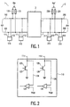
- FIG. 1 shows a first example of a bi-directional signal transmission system in accordance with the invention.
- the bi-directional signal transmission system comprises a first bi-directional signal transmission system 1 and a second bi-directional signal transmission system 2 with an interface device 3 coupled between the two systems.
- the first bi-directional signal transmission system 1 has a bi-directional two-wire bus 101.
- the bus 101 includes a data wire 102 for data signal transport and a clock wire 103 for clock signal transport.
- the data signals and clock signals transmitted on the bus 101 are binary signals.
- Connected to the bus 101 are two stations 110. If desired more stations may be connected to the bus 101. However the number of stations 110 that can be connected to the bus 101 is limited by the total bus capacitance. For example the 400 pF limit specified for the 12C bus sets a practical limit of around 20 stations.
- These stations 110 usually are integrated circuits which may include microcontrollers, general purpose circuits such as LCD drivers, remote I/O ports, RAM, EEPROM or data convertors or application oriented circuits such as digital tuning and signal processing circuits for radio and video systems, or DTMF generators for telephones with tone dialing.
- microcontrollers general purpose circuits such as LCD drivers, remote I/O ports, RAM, EEPROM or data convertors or application oriented circuits such as digital tuning and signal processing circuits for radio and video systems, or DTMF generators for telephones with tone dialing.
- each of these individual stations 110 may be different and perform a different function, for example a microcontroller or a LCD, they all have the same I/O arrangements. For clarity's sake this arrangement will be described with reference to one station 110 which is shown in Figure 2.
- Figure 2 shows a station 110 having a clock l/O 111 and a data I/O 112 which are respectively connected to the clock wire 103 and data wire 102 shown in Figure 1.
- the data l/O 112 is connected to a data output stage 125 and a data input stage 126.
- the data output stage 125 consists of an open -collector transistor 128, which forms the data output of the inner circuitry of the station 110.
- the data input stage 126 consists of a comparator 130 one input of which is connected to the data l/O 12.
- the other input of the comparator 130 is connected to a reference voltage Vhigh.
- the output of the comparator 130 forming the data input of the inner circuitry of the station.
- the clock I/O 111 of the station 110 is connected to a clock output stage 123 and clock input stage 124.
- the clock output stage 124 has an open-collector transistor 127 similar to that of the data output stage 125 and operates in a similar manner.
- the clock input stage 124 has a comparator 129 and reference voltage Vhigh similar to the data input stage 126 and operates in a similar manner.
- the further inner circuit details of the station 110 are not shown.
- the inner circuit details e.g. the microcontroller circuitry or LCD circuitry or other
- the stations 110 communicate with each other by changing the state of the bus wires 102, 103 from HIGH to LOW and vice versa and by detecting whether the bus wires 102,103 are in a HIGH or LOW state.
- the stations 110 detect that a data wire 102 is in a HIGH state when the voltage on the data wire 102 is greater than or equal to a reference voltage Vhigh and detect that the data wire 102 is in a LOW state when the voltage on the data wire 102 is less than said reference voltage Vhigh.
- the stations detect the state of the clock wire 103 in the same manner with respect to said reference voltage Vhigh.
- the stations 110 change the state of the clock and data wires 102,103 by switching on and off the open collector transistors 127 and 128 of the clock and data output stages 123 and 125.
- the bus wires 102 and 103 are pulled up to a supply voltage Vss through pull-up resistors 130 and 131 respectively.
- the supply voltage Vss is chosen to be greater than said reference voltage Vhigh so in this situation the bus wires 102 and 103 are regarded by the stations 110 as being HIGH.
- any one of the stations 110 are able to pull the voltage on the data wire 102 to a voltage Vuu by switching on its open collector transistor 128 of the data output stage 125.
- This data output stage 125 is designed so that the voltage Vuu is less than the said reference voltage Vhigh.
- the voltage of the data wire 102 is Vuu which is less than Vhigh, so the data wire 102 is detected by the stations 110 as being LOW.
- the voltage on the data wire is Vss which is greater than Vhigh, so the data wire 102 is detected by the stations 110 as being HIGH.
- any of the stations 110 are able to pull the voltage on the clock wire 103 to a voltage Vuu by switching on its open collector transistor 127 of the clock output stage 123. As mentioned before this voltage Vuu is below the reference voltage Vhigh. Thus in the on state of the open collector transistor 127, the clock wire 103 is detected by the stations 110 as being LOW and in the off state of said transistors 127, the clock wire 103 is detected by the stations 110 as being HIGH.
- All of the stations 110 connected to the bus 101 have a data and clock output stage 123 and 125. As such anyone of the stations 110 can pull the data or clock wires LOW.
- the data wire 102 will only be HIGH when ALL the open collector transistors 128 of ALL the stations 110 are switched off. Similarly for the clock wire 103.
- Each of the stations 110 has a data and clock input stage 124 and 126 for detecting the state of the bus wires 102 and 103.
- the data input stage 125 shown in Figure 2 has a comparator 130 with one input connected to the data l/O 112 of the station 110. The other input of the comparator 130 is connected to a voltage source having a voltage equivalent to said reference voltage Vhigh. When the voltage on the data wire 102 is above the reference voltage Vhigh the output of the comparator 130 is HIGH and when the voltage on the data wire 102 is below the reference voltage Vhigh the output of the comparator 130 is LOW.
- the clock input stage 123 shown in Figure 2 operates in a similar manner on the clock bus wire 103.
- stations 110 are able to communicate with each other in a binary manner.
- data is transferred from one station 110 to another station 110 in a serial manner under clock control according to the 12C protocol.
- this protocol forms no part of the invention, reference is made to the above mentioned publications where it is described.
- the second bi-directional signal transmission system 2 is similar to the first bi-directional transmission system 1.
- the second bi-directional transmission system 2 has the same features and operates in the same way as the first bi-directional two-wire transmission system and uses the same protocol.
- the second transmission system 2 has a two-wire bi-directional bus 201 comprising a data wire 202 and clock wire 203, stations 210 having clock l/O 211 and data l/O 212 connected respectively to the clock wire 203 and data wire 202 of the bus 201, pull up resistors 230 and 231.
- the stations 110 of the first transmission system 1 and the stations 210 of the second transmission system 2 are similar in nature and operation.
- Station 210 has the same features as the station 110 shown in Figure 2 and operates in the same way.
- the supply voltage Vss, voltage Vuu, reference voltage Vhigh of the first transmission system have a corresponding supply voltage Vss', voltage Vuu', reference voltage Vhigh' in the second transmission system.
- the voltage levels for Vss', Vuu', Vhigh' are the same as Vss, Vuu, Vhigh respectively.
- the actual voltage levels for both the first and second system may differ if desired.
- the voltage supply Vss in the first system may equal 3 volts whereas in the second system the voltage supply Vss' may equal 5 volts.
- stations 210 may be connected to the bus 201 if desired. Though as in the first transmission system 1, there is an upper limit to the number of stations 210 that may be connected to the bus 201.
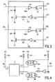
- Figure 3 shows the interface device 3 in detail which is coupled between the first and second bi-directional transmission systems 1 and 2 shown in Figure 1.
- the interface device 3 consists of a separate data interface stage 310 and a clock interface stage 320.
- a data l/O 311 and a clock I/O 321 of the interface device 3 are respectively connected to the data wire 102 and the clock wire 103 shown in Figure 1.
- the interface device 3 also has a data transmitting output 312 and a data receiving input 313 which are both connected to the data wire 202 as shown in Figure 1.
- the interface device 3 further has a clock transmitting output 322 and a clock receiving input 323 which are both connected to the clock wire 203 as shown in Figure 1.
- the data I/O 311 of the data interface stage 310 is connected to an input of a comparator 314, the other input of which is connected to a reference voltage Vmed.
- the output of the comparator 314 is connected to the base of an open collector transistor 315, the collector of which is connected to the data transmitting output 312, and the emitter to earth.
- the data receiving input 313 of the data interface stage 310 is connected to an invertor 316 which is connected to the base of an open collector transistor 318 via a resistor 317.
- the data l/O 311 of the data interface stage 310 is also connected to the anode of a diode 319, the cathode of which is connected to the collector of the transistor 318.
- the diode 319 acting as a voltage source.
- the emitter of the transistor 318 is connected to earth.
- the data wire 102 and data l/O 311 were floating HIGH at voltage Vss
- the open collector transistor 318 when the open collector transistor 318 is switched on, the data l/O 311 and data wire 102 are pulled down to a voltage Vtt.
- the reference voltage Vmed and Voltage Vtt are chosen such that Vss > Vhigh > Vtt > Vmed > Vuu.
- the clock l/O 321 of the clock interface stage 320 is connected to an input of a comparator 324, the other input of which is connected to a reference voltage Vmed.
- the output of the comparator 324 is connected to the base of an open collector transistor 325, the collector of which is connected to the clock transmitting output 322, and the emitter to earth.
- the clock receiving input 323 of the clock interface stage 320 is connected to an invertor 326 which is connected to the base of an open collector transistor 328 via a resistor 327.
- the clock l/O 321 of the clock interface stage is also connected to the anode of a diode 329, the cathode of which is connected to the collector of the transistor 328.
- the diode 329 acting as a voltage source.
- the emitter of the transistor 328 is connected to earth.
- the clock wire 103, clock interface stage 320 and clock wire 203 system has the same features as, and operates in the same manner as the data wire 102, data interface stage 310 and data wire 202 system.
- the voltages levels are the same for both.
- the clock interface stage 320 operates in the same manner and need not be described.
- the later will pull the data transmitting output 312 LOW to Vuu'.
- the transmitting data output 312 will be pulled LOW to Vuu' by the station 210 but NOT by the interface device 3.
- the station 210 releases the data wire 202, that is switches off its transistor 128, the data wire 202 will go HIGH again.
- all the stations 210 are able to detect that the data wire 202 is LOW as Vuu' ⁇ Vhigh' and all the stations 110 are able to detect that the data wire 102 is LOW as Vtt ⁇ Vhigh.
- the voltage on the data l/O 311 When a station 110 pulls down the voltage on the data wire 102 to a voltage Vuu, the voltage on the data l/O 311 will be Vuu. As the voltage Vuu is less than Vmed, the comparator 314 switches on the open collector transistor 315. In these circumstances the data transmitting output 312 and data wire 202 of the second system will be pulled down to the voltage Vuu' by the open collector transistor 315. As the data receiving input 313 is connected to the data transmitting output 312, then the voltage on the invertor 316 will be Vuu'. In these circumstances the output of the invertor 316 will be high and the open collector transistor 318 will be turned on.
- the data wire 102 is already pulled down to the voltage Vuu and due to the circuit arrangement of the bus the open collector transistor 318 is unable to pull the voltage on the data wire 102 up to Vtt.
- the voltage on the data wire 102 remains at Vuu.
- All the stations 110 are able to detect that the data wire is LOW as Vuu ⁇ Vhigh and all the stations 210 are able to detect that the data wire 202 is LOW as Vuu' ⁇ Vhigh'.
- the station 110 releases the data wire 102, that is switches off the transistor 128, the data wire 102 will initially pull up to voltage Vtt.
- the comparator 314 will switch off the open collector transistor 315 and the data transmitting output 312 will float HIGH to voltage Vss'. This in turn will cause the transistor 318 to switch off and the data wire 102 will finally float HIGH to Vss.
- the following is a table summarizing the above operation of the interface device 3 and showing the state of the data receiving input (RxD) 313, data l/O (Di/o) 311 and data transmitting output (TxD) 312 as detected by their relevant stations 110 and 210.
- the arrow indicates the signal propagation.
- a logic HIGH will propagate in both directions, a logic LOW will propagate from the data I/O 311 to the data transmitting output 312, and a logic LOW will propagate from the data receiving input 313 to the data I/O 311, but a logic LOW will not propagate from the data receiving input 313 to the data transmitting output 312 because of the medium voltage level that is then present on the data l/O 311. Whilst the medium voltage level on the data I/O 311 is detected by the stations 110 as being LOW, the interface device 3 detects the medium voltage level as being HIGH. It is by this means the latching is prevented.
- Figure 4 shows a second embodiment of the bi-directional signal transmission system in accordance with the invention having an interface device as shown in Figure 3.
- the interface device 3 is coupled by its data l/O 311 to the data wire 102 of a transmission system 1 of the type shown in Figure 1.
- the interface device is also coupled to the data wire 202 of a transmission system 2 of the type shown in Figure 1. Only the data wire 102 and data wire 202 of the first and second transmission systems and the data interface stage of the interface device 3 are shown in Figure 4.
- the clock wires 103, 203 of the first and second transmission systems and the clock interface stage of the interface device 3 are coupled and operate in the same manner as the data wires 102,202 and the data interface stage and as such are not shown.
- the data transmitting output 312 is coupled to the data wire 202 via an opto-coupler 432.
- the data wire 202 is coupled to the data receiving input 313 via an invertor 433, resistor 434 and an opto-coupler 435.
- the data receiving input 313 is coupled to the supply voltage Vss' by a pull up resistor 430.
- the data transmitting output 312 is coupled to the supply voltage Vss' via the opto-coupler 432 and pull up resistor 431.
- the diode of the opto-coupler 432 In operation when the data transmitting output 312 is HIGH (the transistor 315 of Figure 3 is off), the diode of the opto-coupler 432 is not on and the photo-transistor of the opto-coupler is an off state. Thus the data wire 202 may float HIGH to Vss'.
- the voltage on the data transmitting output 312 is LOW (the transistor 315 is on) the diode of the opto-coupler 432 is on, and the photo-transistor of the opto-coupler is an on state and the data wire 202 will be pulled LOW to a voltage Vuu'.
- the interface device 3 is connected via the data l/O to a first transmission system of the type shown in figure 1.
- the data transmitting output 312 and data receiving input 313 are connected to the respective input and output of a differential bus interface device to, for example, a CAN bus using an interface IC.
- the input and output of the CAN bus interface IC are connected to the respective data transmitting outputs 312 and data receiving inputs 313 of further interface devices 3, the data I/O of which are connected to further transmission systems of the type shown in figure 1.
- the interface device 3 has both a data interface stage and clock interface stage which operate in the same manner and are coupled to respective data wires and clock wires.
- the clock bus wires may also be configured as a single master system and as such a clock buffer different to the clock interface stage may be used together with a data interface stage of the type described herein.
Landscapes
- Engineering & Computer Science (AREA)
- Signal Processing (AREA)
- Computer Networks & Wireless Communication (AREA)
- Power Engineering (AREA)
- Small-Scale Networks (AREA)
- Bidirectional Digital Transmission (AREA)
- Compositions Of Oxide Ceramics (AREA)
- Variable-Direction Aerials And Aerial Arrays (AREA)
- Communication Control (AREA)
- Dc Digital Transmission (AREA)
Claims (11)
- Zweiwegsignalübertragungsanordnung, die Folgendes umfasst:wobei die Schnittstellenvorrichtung Folgendes umfasst:einen ersten Zweiweg-Signalpfad (101), der Mittel zum Erzeugen eines logisch hohen Zustand auf ihm umfasst, eine oder mehrere erste Stationen (110), die mit dem ersten Zweiweg-Signalpfad gekoppelt sind und jeweils einen logisch niedrigen Zustand auf dem ersten Zweiweg-Signalpfad erzeugen können;eine Schnittstellenvorrichtung (3), die mit dem ersten Zweiweg-Signalpfad gekoppelt ist und über einen Empfangseingang (313) und einen Sendeausgang (312) verfügt;einen zweiten Zweiweg-Signalpfad (201), der mit dem Empfangseingang und dem Sendeausgang der Schnittstellenvorrichtung gekoppelt ist;wobei die eine oder mehreren ersten Stationen (110) so ausgelegt sind, dass sie den mittleren und den niedrigen logischen Zustand auf dem ersten Zweiweg-Signalpfad als LOW und den hohen logischen Zustand auf dem ersten Zweiweg-Signalpfad als HIGH erkennen.erste Mittel (316 - 319) zum Erzeugen eines mittleren logischen Zustands auf dem ersten Zweiweg-Signalpfad in Reaktion auf einen niedrigen logischen Zustand am Empfangseingang,zweite Mittel (314, 315) zum Erzeugen eines niedrigen logischen Zustands auf dem ersten Zweiweg-Signalpfad in Reaktion auf den genannten niedrigen logischen Zustand am Sendeausgang, und sonst zum Erzeugen eines hohen logischen Zustands an dem genannten Sendeausgang,
- Zweiwegsignalübertragungsanordnung nach Anspruch 1, wobei die ersten Mittel der Schnittstellenvorrichtung einen Inverter enthalten, dessen Eingang mit dem Empfangseingang und dessen Ausgang mit der Basis eines Transistors mit offenem Kollektor verbunden ist, und eine Spannungsquelle, die zwischen den ersten Zweiweg-Signalpfad und den Transistor mit offenem Kollektor geschaltet ist, wobei der Inverter in Reaktion auf einen hohen logischen Zustand am Empfangseingang den Transistor mit offenem Kollektor ausschaltet und in Reaktion auf den genannten niedrigen logischen Zustand am Empfangseingang den Transistor mit offenem Kollektor einschaltet, wobei der Transistor mit offenem Kollektor im eingeschalteten Zustand den ersten Zweiweg-Signalpfad auf den genannten mittleren logischen Zustand "herunterzieht" und im ausgeschalteten Zustand den ersten Zweiweg-Signalpfad auf dem genannten hohen logischen Zustand belässt.
- Zweiwegsignalübertragungsanordnung nach jeglichem der vorhergehenden Ansprüche, wobei die zweiten Mittel der Schnittstellenvorrichtung einen Komparator enthalten, dessen einer Eingang mit dem ersten Zweiweg-Signalpfad und dessen anderer Eingang mit einer Bezugsspannungsquelle Vmed gekoppelt ist, wobei der Ausgang eines Transistors mit offenem Kollektor des Komparators mit dem Sendeausgang der Schnittstellenvorrichtung gekoppelt ist und die zweiten Mittel am Sendeausgang den genannten niedrigen logischen Zustand erzeugen, wenn der logische Zustand auf dem ersten Zweiweg-Signalpfad unter der Bezugsspannung Vmed liegt, und am Sendeausgang einen genannten hohen logischen Zustand erzeugen, wenn der logische Zustand auf dem ersten Zweiweg-Signalpfad höher als die Bezugsspannung Vmed ist.
- Zweiwegsignalübertragungsanordnung nach jeglichem der vorhergehenden Ansprüche, wobei der Sendeausgang und der Empfangsausgang der Schnittstellenvorrichtung direkt mit dem zweiten Zweiweg-Signalpfad verbunden sind.
- Zweiwegsignalübertragungsanordnung nach jeglichem der Ansprüche 1 - 3, wobei der Sendeausgang der Schnittstellenvorrichtung mit dem zweiten Zweiweg-Signalpfad über einen ersten Optokoppler gekoppelt und der zweite Zweiweg-Signalpfad über einen zweiten Optokoppler in Reihe mit dem Empfangseingang geschaltet ist.
- Zweiwegsignalübertragungsanordnung nach jeglichem der Ansprüche 1 - 3, wobei der Sendeausgang der Schnittstellenvorrichtung über einen differentiellen Bus mit dem Empfangseingang der genannten weiteren Schnittstellenvorrichtung gekoppelt ist, die mit dem genannten zweiten Zweiweg-Signalpfad gekoppelt ist, und der Sendeausgang der genannten weiteren Schnittstellenvorrichtung über den differentiellen Bus mit dem Empfangseingang der ersten genannten Schnittstellenvorrichtung gekoppelt ist.
- Zweiwegsignalübertragungsanordnung nach jeglichem der vorhergehenden Ansprüche, wobei der erste und der zweite Zweiweg-Signalpfad Datenpfade sind.
- Zweiwegsignalübertragungsanordnung nach jeglichem der Ansprüche 1 - 6, wobei der erste und der zweite Zweiweg-Signalpfad sowohl einen Datensignalpfad als auch einen Taktsignalpfad beinhalten und die Schnittstellenvorrichtung eine erste Schnittstellenstufe und eine zweite Schnittstellenstufe umfasst, wobei der Datensignalpfad des ersten Zweiweg-Signalpfades mit dem Datensignalpfad des genannten zweiten Zweiweg-Signalpfades über die erste Schnittstellenstufe und der Taktsignalpfad des ersten Zweiweg-Signalpfades mit dem Taktsignalpfad des genannten zweiten Zweiweg-Signalpfades über die zweite Schnittstellenstufe verbunden ist
- Schnittstellenvorrichtung (3) zum Einsatz in einer Zweiwegsignalübertragungsanordnung, wobei die Anordnung Folgendes umfasst:wobei die Schnittstellenvorrichtung Folgendes umfasst:einen ersten Zweiweg-Signalpfad (101), der Mittel zum Erzeugen eines logisch hohen Zustandes auf ihm umfasst, eine oder mehrere erste Stationen (110), die mit dem ersten Zweiweg-Signalpfad gekoppelt sind und jeweils einen logisch niedrigen Zustand auf dem ersten Zweiweg-Signalpfad erzeugen können,einen zweiten Zweiweg-Signalpfad (201), wobei die eine oder mehreren ersten Stationen so ausgelegt sind, dass sie einen mittleren logischen Zustand und den niedrigen logischen Zustand auf dem ersten Zweiweg-Signalpfad als LOW und den hohen logischen Zustand auf dem ersten Zweiweg-Signalpfad als HIGH erkennen, wobei die Schnittstellenvorrichtung so ausgelegt ist, dass sie mit dem ersten Zweiweg-Signalpfad gekoppelt ist und einen Empfangseingang (313) und einen Sendeausgang (312) aufweist, die so ausgelegt sind, dass sie mit dem zweiten Zweiweg-Signalpfad gekoppelt sind,erste Mittel (316 - 319) zum Erzeugen des genannten mittleren logischen Zustands auf dem ersten Zweiweg-Signalpfad in Reaktion auf einen niedrigen logischen Zustand am Empfangseingang,zweite Mittel (314, 315) zum Erzeugen eines niedrigen logischen Zustands auf dem ersten Zweiweg-Signalpfad in Reaktion auf den genannten niedrigen logischen Zustand am Sendeausgang, und sonst zum Erzeugen eines hohen logischen Zustands an dem genannten Sendeausgang.
- Schnittstellenvorrichtung nach Anspruch 9, wobei die ersten Mittel der Schnittstellenvorrichtung einen Inverter enthalten, dessen Eingang mit dem Empfangseingang und dessen Ausgang mit der Basis eines Transistors mit offenem Kollektor verbunden ist, und eine Spannungsquelle, die zwischen den ersten Zweiweg-Signalpfad und den Transistor mit offenem Kollektor geschaltet ist, wobei der Inverter in Reaktion auf einen hohen logischen Zustand am Empfangseingang den Transistor mit offenem Kollektor ausschaltet und in Reaktion auf den genannten niedrigen logischen Zustand am Empfangseingang den Transistor mit offenem Kollektor einschaltet, wobei der Transistor mit offenem Kollektor im eingeschalteten Zustand den ersten Zweiweg-Signalpfad auf den genannten mittleren logischen Zustand "herunterzieht" und im ausgeschalteten Zustand den ersten Zweiweg-Signalpfad auf dem genannten hohen logischen Zustand belässt.
- Schnittstellenvorrichtung nach Anspruch 9 oder 10, wobei die zweiten Mittel der Schnittstellenvorrichtung einen Komparator enthalten, dessen einer Eingang mit dem ersten Zweiweg-Signalpfad und dessen anderer Eingang mit einer Bezugsspannungsquelle Vmed gekoppelt ist, wobei der Ausgang eines Transistors mit offenem Kollektor des Komparators mit dem Sendeausgang der Schnittstellenvorrichtung gekoppelt ist und die zweiten Mittel am Sendeausgang den genannten niedrigen logischen Zustand erzeugen, wenn der logische Zustand auf dem ersten Zweiweg-Signalpfad unter der Bezugsspannung Vmed liegt, und am Sendeausgang einen genannten hohen logischen Zustand erzeugen, wenn der logische Zustand auf dem ersten Zweiweg-Signalpfad höher als die Bezugsspannung Vmed ist.
Applications Claiming Priority (4)
| Application Number | Priority Date | Filing Date | Title |
|---|---|---|---|
| AUPN7047/95 | 1995-12-11 | ||
| AUPN704795 | 1995-12-11 | ||
| AUPN7047A AUPN704795A0 (en) | 1995-12-11 | 1995-12-11 | Bi-directional signal transmission system |
| PCT/IB1996/001379 WO1997022184A2 (en) | 1995-12-11 | 1996-12-06 | Bi-directional signal transmission system |
Publications (2)
| Publication Number | Publication Date |
|---|---|
| EP0808530A2 EP0808530A2 (de) | 1997-11-26 |
| EP0808530B1 true EP0808530B1 (de) | 2002-11-13 |
Family
ID=3791367
Family Applications (1)
| Application Number | Title | Priority Date | Filing Date |
|---|---|---|---|
| EP96939260A Expired - Lifetime EP0808530B1 (de) | 1995-12-11 | 1996-12-06 | Zweiwegsignalübertragungsanordnung |
Country Status (8)
| Country | Link |
|---|---|
| US (1) | US6014040A (de) |
| EP (1) | EP0808530B1 (de) |
| JP (1) | JP3639600B2 (de) |
| KR (1) | KR100463886B1 (de) |
| AT (1) | ATE227904T1 (de) |
| AU (2) | AUPN704795A0 (de) |
| DE (1) | DE69624791T2 (de) |
| WO (1) | WO1997022184A2 (de) |
Families Citing this family (23)
| Publication number | Priority date | Publication date | Assignee | Title |
|---|---|---|---|---|
| TW362178B (en) * | 1997-01-30 | 1999-06-21 | Nxp Bv | Electronic apparatus |
| US6265951B1 (en) | 1997-11-15 | 2001-07-24 | Cybex Computer Products Corporation | Method and apparatus for equalizing channel characteristics in a computer extension system |
| US6185643B1 (en) | 1997-11-15 | 2001-02-06 | Cybex Computer Products Corporation | Method and apparatus for extending the range between a computer and computer peripherals |
| US6078974A (en) * | 1998-04-08 | 2000-06-20 | Cybex Computer Products Corporation | Method and apparatus for extension of bi-directional open collector signals in a multiplexed data transmission system |
| KR100659218B1 (ko) * | 1998-09-03 | 2006-12-20 | 소니 일렉트로닉스 인코포레이티드 | 임피던스 격리 확장 회로를 이용한 장치 제어 시스템용 감축마이크로프로세서 기기 및 방법 |
| FR2788147B1 (fr) * | 1998-12-30 | 2001-03-16 | Jean Gasnault | Lecteur de normes et codes stockes sous forme electronique |
| EP1050824A3 (de) * | 1999-04-22 | 2004-01-28 | Matsushita Electric Industrial Co., Ltd. | Bidirektionale Signalübertragungsschaltung und Bussystem |
| US6686774B1 (en) * | 2001-07-19 | 2004-02-03 | Raza Microelectronics, Inc. | System and method for a high speed, bi-directional, zero turnaround time, pseudo differential bus capable of supporting arbitrary number of drivers and receivers |
| US7062596B2 (en) * | 2001-08-22 | 2006-06-13 | Avocent Corporation | Self-synchronizing half duplex matrix switch |
| US7088137B2 (en) * | 2004-05-04 | 2006-08-08 | International Business Machines Corporation | System, method and program product for extending range of a bidirectional data communication bus |
| US7348803B2 (en) * | 2005-06-24 | 2008-03-25 | Integrated Electronic Solutions Pty. Ltd. | Bi-directional bus buffer |
| KR100680012B1 (ko) * | 2006-03-22 | 2007-02-09 | 연세대학교 산학협력단 | 광 검출 트랜지스터를 구비한 rof 시스템 |
| US7417464B2 (en) * | 2006-09-22 | 2008-08-26 | Integrated Electronic Solutions Pty. Ltd | Bi-directional signal transmission system |
| US7840734B2 (en) * | 2006-12-21 | 2010-11-23 | Hendon Semiconductors Pty Ltd. | Simple bus buffer |
| US7808277B2 (en) * | 2008-09-18 | 2010-10-05 | Hewlett-Packard Development Company, L.P. | Bidirectional signal separation module for a bus converter |
| IT1391688B1 (it) * | 2008-10-30 | 2012-01-17 | Indesit Co Spa | Dispositivo adattatore per sistema di comunicazione bidirezionale e relativo sistema |
| CN101576868B (zh) * | 2009-05-18 | 2012-07-04 | 艾默生网络能源有限公司 | 一种i2c总线通信驱动电路 |
| CN102289420B (zh) * | 2011-06-28 | 2013-06-12 | 电子科技大学 | 一种简易单总线接口转换电路及其应用的数据采集系统 |
| US9256570B2 (en) * | 2011-08-05 | 2016-02-09 | Linear Technology Corporation | I2C isolated, bidirectional communication system with isolated domain current source pull-ups |
| US8803117B2 (en) | 2012-03-29 | 2014-08-12 | Motorola Solutions, Inc. | Apparatus and method for non-latching, bi-directional communication over an electrically isolated data link |
| KR101286300B1 (ko) * | 2012-05-31 | 2013-07-19 | (주) 네오큐 | 순번대기 시스템의 과전압/과전류 방지장치 및 그 방법 |
| CN103441780A (zh) * | 2013-08-16 | 2013-12-11 | 北京汉柏科技有限公司 | Rs-485自动切换方向的通讯电路 |
| CN109412575B (zh) * | 2018-11-30 | 2022-09-27 | 中国电子科技集团公司第四十四研究所 | 一种传输方向可选的高速数字型光电耦合器 |
Family Cites Families (2)
| Publication number | Priority date | Publication date | Assignee | Title |
|---|---|---|---|---|
| US5428800A (en) * | 1991-10-30 | 1995-06-27 | I-Cube, Inc. | Input/output (I/O) bidirectional buffer for interfacing I/O ports of a field programmable interconnection device with array ports of a cross-point switch |
| JP3025118B2 (ja) * | 1992-10-26 | 2000-03-27 | 株式会社日立製作所 | 半導体集積回路装置と情報処理システム |
-
1995
- 1995-12-11 AU AUPN7047A patent/AUPN704795A0/en not_active Abandoned
-
1996
- 1996-12-06 AT AT96939260T patent/ATE227904T1/de not_active IP Right Cessation
- 1996-12-06 DE DE69624791T patent/DE69624791T2/de not_active Expired - Lifetime
- 1996-12-06 JP JP52189397A patent/JP3639600B2/ja not_active Expired - Fee Related
- 1996-12-06 EP EP96939260A patent/EP0808530B1/de not_active Expired - Lifetime
- 1996-12-06 WO PCT/IB1996/001379 patent/WO1997022184A2/en not_active Ceased
- 1996-12-06 KR KR1019970705520A patent/KR100463886B1/ko not_active Expired - Fee Related
- 1996-12-09 US US08/767,597 patent/US6014040A/en not_active Expired - Lifetime
- 1996-12-11 AU AU75307/96A patent/AU710082B2/en not_active Ceased
Also Published As
| Publication number | Publication date |
|---|---|
| DE69624791T2 (de) | 2003-07-03 |
| AUPN704795A0 (en) | 1996-01-11 |
| WO1997022184A2 (en) | 1997-06-19 |
| AU7530796A (en) | 1997-06-19 |
| WO1997022184A3 (en) | 1997-07-31 |
| KR19980702125A (ko) | 1998-07-15 |
| AU710082B2 (en) | 1999-09-16 |
| JP3639600B2 (ja) | 2005-04-20 |
| US6014040A (en) | 2000-01-11 |
| DE69624791D1 (de) | 2002-12-19 |
| JPH11500893A (ja) | 1999-01-19 |
| ATE227904T1 (de) | 2002-11-15 |
| KR100463886B1 (ko) | 2005-04-08 |
| EP0808530A2 (de) | 1997-11-26 |
Similar Documents
| Publication | Publication Date | Title |
|---|---|---|
| EP0808530B1 (de) | Zweiwegsignalübertragungsanordnung | |
| US7088137B2 (en) | System, method and program product for extending range of a bidirectional data communication bus | |
| US4280221A (en) | Digital data communication system | |
| JPH01501275A (ja) | トランシーバ用ターミネータ | |
| US8368426B2 (en) | Low voltage differential signal driving circuit and digital signal transmitter | |
| GB2131658A (en) | Communication bus | |
| CN103227656A (zh) | 双向收发器及方法 | |
| EP1230683A2 (de) | I2c opto-isolator-schaltung | |
| US4648105A (en) | Register circuit for transmitting and receiving serial data | |
| US7359433B1 (en) | Data transmission system | |
| EP0787327B1 (de) | Datenverarbeitungssystem mit einer asynchrongesteuerten pipeline | |
| EP1410589B1 (de) | Sender mit aktivem differenzabschluss | |
| WO2000051256A1 (en) | Bus driver with data dependent drive strength control logic | |
| US7353308B2 (en) | Avoiding oscillation in self-synchronous bi-directional communication system | |
| CN216819835U (zh) | 单线隔离通讯装置及系统 | |
| US6661255B2 (en) | Interface circuit | |
| CN213042273U (zh) | 二线制串行总线接口转换为单线半双工总线接口的电路 | |
| US7535256B2 (en) | Cross-level digital signal transmission device | |
| US12040794B2 (en) | Semiconductor integrated circuits that support enhanced signal multiplexing operations for I/O buffers | |
| CN218124699U (zh) | 一种单线串行收发电路 | |
| CN113726622A (zh) | 一种通信设备、塔放设备及其自动切换电路 | |
| US12494951B2 (en) | Device for CAN bus | |
| CN111090602B (zh) | 一种uart串口收发自适应方法和系统 | |
| CN117061267A (zh) | 一种高速率串行通讯电路 | |
| SU1520532A1 (ru) | Устройство дл сопр жени двух ЭВМ |
Legal Events
| Date | Code | Title | Description |
|---|---|---|---|
| PUAI | Public reference made under article 153(3) epc to a published international application that has entered the european phase |
Free format text: ORIGINAL CODE: 0009012 |
|
| AK | Designated contracting states |
Kind code of ref document: A2 Designated state(s): AT CH DE ES FR GB IT LI |
|
| 17P | Request for examination filed |
Effective date: 19971219 |
|
| GRAG | Despatch of communication of intention to grant |
Free format text: ORIGINAL CODE: EPIDOS AGRA |
|
| 17Q | First examination report despatched |
Effective date: 20020118 |
|
| GRAG | Despatch of communication of intention to grant |
Free format text: ORIGINAL CODE: EPIDOS AGRA |
|
| GRAH | Despatch of communication of intention to grant a patent |
Free format text: ORIGINAL CODE: EPIDOS IGRA |
|
| GRAH | Despatch of communication of intention to grant a patent |
Free format text: ORIGINAL CODE: EPIDOS IGRA |
|
| GRAA | (expected) grant |
Free format text: ORIGINAL CODE: 0009210 |
|
| AK | Designated contracting states |
Kind code of ref document: B1 Designated state(s): AT CH DE ES FR GB IT LI |
|
| PG25 | Lapsed in a contracting state [announced via postgrant information from national office to epo] |
Ref country code: LI Free format text: LAPSE BECAUSE OF FAILURE TO SUBMIT A TRANSLATION OF THE DESCRIPTION OR TO PAY THE FEE WITHIN THE PRESCRIBED TIME-LIMIT Effective date: 20021113 Ref country code: IT Free format text: LAPSE BECAUSE OF FAILURE TO SUBMIT A TRANSLATION OF THE DESCRIPTION OR TO PAY THE FEE WITHIN THE PRE;WARNING: LAPSES OF ITALIAN PATENTS WITH EFFECTIVE DATE BEFORE 2007 MAY HAVE OCCURRED AT ANY TIME BEFORE 2007. THE CORRECT EFFECTIVE DATE MAY BE DIFFERENT FROM THE ONE RECORDED.SCRIBED TIME-LIMIT Effective date: 20021113 Ref country code: CH Free format text: LAPSE BECAUSE OF FAILURE TO SUBMIT A TRANSLATION OF THE DESCRIPTION OR TO PAY THE FEE WITHIN THE PRESCRIBED TIME-LIMIT Effective date: 20021113 Ref country code: AT Free format text: LAPSE BECAUSE OF FAILURE TO SUBMIT A TRANSLATION OF THE DESCRIPTION OR TO PAY THE FEE WITHIN THE PRESCRIBED TIME-LIMIT Effective date: 20021113 |
|
| REF | Corresponds to: |
Ref document number: 227904 Country of ref document: AT Date of ref document: 20021115 Kind code of ref document: T |
|
| REG | Reference to a national code |
Ref country code: GB Ref legal event code: FG4D |
|
| REG | Reference to a national code |
Ref country code: CH Ref legal event code: EP |
|
| REF | Corresponds to: |
Ref document number: 69624791 Country of ref document: DE Date of ref document: 20021219 |
|
| ET | Fr: translation filed | ||
| PG25 | Lapsed in a contracting state [announced via postgrant information from national office to epo] |
Ref country code: ES Free format text: LAPSE BECAUSE OF FAILURE TO SUBMIT A TRANSLATION OF THE DESCRIPTION OR TO PAY THE FEE WITHIN THE PRESCRIBED TIME-LIMIT Effective date: 20030529 |
|
| REG | Reference to a national code |
Ref country code: CH Ref legal event code: PL |
|
| PLBE | No opposition filed within time limit |
Free format text: ORIGINAL CODE: 0009261 |
|
| STAA | Information on the status of an ep patent application or granted ep patent |
Free format text: STATUS: NO OPPOSITION FILED WITHIN TIME LIMIT |
|
| 26N | No opposition filed |
Effective date: 20030814 |
|
| REG | Reference to a national code |
Ref country code: GB Ref legal event code: 732E Free format text: REGISTERED BETWEEN 20090305 AND 20090311 |
|
| PGFP | Annual fee paid to national office [announced via postgrant information from national office to epo] |
Ref country code: FR Payment date: 20081212 Year of fee payment: 13 |
|
| REG | Reference to a national code |
Ref country code: FR Ref legal event code: ST Effective date: 20100831 |
|
| PG25 | Lapsed in a contracting state [announced via postgrant information from national office to epo] |
Ref country code: FR Free format text: LAPSE BECAUSE OF NON-PAYMENT OF DUE FEES Effective date: 20091231 |
|
| REG | Reference to a national code |
Ref country code: GB Ref legal event code: 732E Free format text: REGISTERED BETWEEN 20101007 AND 20101013 |
|
| PGFP | Annual fee paid to national office [announced via postgrant information from national office to epo] |
Ref country code: GB Payment date: 20141121 Year of fee payment: 19 |
|
| PGFP | Annual fee paid to national office [announced via postgrant information from national office to epo] |
Ref country code: DE Payment date: 20150212 Year of fee payment: 19 |
|
| REG | Reference to a national code |
Ref country code: DE Ref legal event code: R119 Ref document number: 69624791 Country of ref document: DE |
|
| GBPC | Gb: european patent ceased through non-payment of renewal fee |
Effective date: 20151206 |
|
| PG25 | Lapsed in a contracting state [announced via postgrant information from national office to epo] |
Ref country code: GB Free format text: LAPSE BECAUSE OF NON-PAYMENT OF DUE FEES Effective date: 20151206 Ref country code: DE Free format text: LAPSE BECAUSE OF NON-PAYMENT OF DUE FEES Effective date: 20160701 |