EP0808023B1 - Strombitzelle und stromgeschaltetes Netzwerk mit derartigen Zellen - Google Patents
Strombitzelle und stromgeschaltetes Netzwerk mit derartigen Zellen Download PDFInfo
- Publication number
- EP0808023B1 EP0808023B1 EP19970401063 EP97401063A EP0808023B1 EP 0808023 B1 EP0808023 B1 EP 0808023B1 EP 19970401063 EP19970401063 EP 19970401063 EP 97401063 A EP97401063 A EP 97401063A EP 0808023 B1 EP0808023 B1 EP 0808023B1
- Authority
- EP
- European Patent Office
- Prior art keywords
- detecting
- transistor
- cell
- status
- bit
- Prior art date
- Legal status (The legal status is an assumption and is not a legal conclusion. Google has not performed a legal analysis and makes no representation as to the accuracy of the status listed.)
- Expired - Lifetime
Links
- 230000000295 complement effect Effects 0.000 claims description 77
- 238000010276 construction Methods 0.000 claims description 5
- 230000005669 field effect Effects 0.000 claims description 3
- 230000008901 benefit Effects 0.000 description 7
- 238000010586 diagram Methods 0.000 description 4
- 238000007667 floating Methods 0.000 description 4
- 238000000034 method Methods 0.000 description 3
- 238000012856 packing Methods 0.000 description 3
- 239000003990 capacitor Substances 0.000 description 2
- 230000008878 coupling Effects 0.000 description 2
- 238000010168 coupling process Methods 0.000 description 2
- 238000005859 coupling reaction Methods 0.000 description 2
- 238000005516 engineering process Methods 0.000 description 2
- 239000000758 substrate Substances 0.000 description 2
- 230000001052 transient effect Effects 0.000 description 2
- XUIMIQQOPSSXEZ-UHFFFAOYSA-N Silicon Chemical compound [Si] XUIMIQQOPSSXEZ-UHFFFAOYSA-N 0.000 description 1
- 230000004913 activation Effects 0.000 description 1
- 238000004458 analytical method Methods 0.000 description 1
- 238000004519 manufacturing process Methods 0.000 description 1
- 229910052710 silicon Inorganic materials 0.000 description 1
- 239000010703 silicon Substances 0.000 description 1
- 230000007704 transition Effects 0.000 description 1
Images

Classifications
-
- H—ELECTRICITY
- H03—ELECTRONIC CIRCUITRY
- H03K—PULSE TECHNIQUE
- H03K5/00—Manipulating of pulses not covered by one of the other main groups of this subclass
- H03K5/22—Circuits having more than one input and one output for comparing pulses or pulse trains with each other according to input signal characteristics, e.g. slope, integral
- H03K5/24—Circuits having more than one input and one output for comparing pulses or pulse trains with each other according to input signal characteristics, e.g. slope, integral the characteristic being amplitude
- H03K5/2472—Circuits having more than one input and one output for comparing pulses or pulse trains with each other according to input signal characteristics, e.g. slope, integral the characteristic being amplitude using field effect transistors
- H03K5/2481—Circuits having more than one input and one output for comparing pulses or pulse trains with each other according to input signal characteristics, e.g. slope, integral the characteristic being amplitude using field effect transistors with at least one differential stage
Definitions
- the present invention relates to the structure of a current bit cell intended to be used in switched current networks as, for example, in the implementation of analogue/digital converters ADCs.
- Another advantage of this structure is the symmetry of its topology, which makes it suitable for the implementation of differential networks whose characteristics, connected with the unsusceptibility to noise, are attractive for the implementation of analogue circuits.
- One known means of ensuring monotonicity is to add an element to each increment of a digital code.
- Document EP-A-0136229 discloses a sense amplifier which selects one of a plurality of pairs of complementary input signals and generates an output signal corresponding to a selected pair of complementary input signals.
- the object of the invention is to overcome the aforementioned drawbacks of known current bit cell structures.
- a current bit cell used in the construction of a switched network comprising a current source, FET means for detecting the presence of a digital signal bit and FET means for detecting at least one command signal so as to provide first FET means for controlling on a first output of the cell, the appearance of a current delivered by the current source as a function of the digital signal applied to the said cell and of the said at least one command signal, characterized in that it furthermore includes FET means for detecting the presence of a bit complementary to the bit of the digital signal and FET means for detecting the complement of the said at least one command signal, so as to provide second FET means for controlling on a second output of the cell as a function of the complementary digital signal and of said complement of said at least one command signal the appearance of a current delivered by the current source which is the complement of the current delivered on the first output, the said FET means for detecting the presence of bits and of the said at least one command signal, the said FET means for detecting the presence of complementary bits and of complementary signals, the said FET means for
- a further subject of the invention is a switched current network, characterized in that it is formed of current bit cells of the type defined above, laid out in rows and columns, the first and second outputs of the said cells being respectively connected together and in that the said cells of the network are laid out around the center of the network divided into four quadrants in such a way as to be commanded in accordance with a sequence in which command of a cell situated in a quadrant is followed by command of a cell situated in a quadrant symmetric with the previous quadrant with respect to the center of the network.
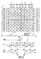
- This current bit cell includes a decoding part with a complex gate G1 and an invertor I1 in CMOS technology, employing four N-channel transistors and four P-channel transistors, and the current bit cell proper comprising a current source P1 and two switches P2 and P3, formed by three P-channel transistors, which makes eleven transistors in total.
- a network can be produced as an array of Y rows and X columns, and the decoding scheme represented in Figure 2 is then as follows.
- All the current bit cells of a single row are connected to the same row-decoding signal L and to a full row-decoding signal Lc, while all the rows of current bits in a single column are connected to a column decoding signal Bit.
- a current bit cell such as the one in Figure 1 is defined as active when the current flows through the output S1.
- each individual current bit cell can be activated when its row (signal L) and its column (signal Bit) are active, whereas all the current bit cells of a row are activated when the entire row (signal Lc) is active.
- This network is organised in the form of a network of Y rows and X columns.
- the numbering of its cells from 0 to 63 expresses their order of command according to a sequence in which the commanding of a cell, such that the cell No. 0 located in a quadrant I of the network is followed by the commanding of a cell such as the cell No. 1 located in a quadrant III which is symmetrical to the previous quadrant with respect to the centre of the network manifested by the intersection of the lines V and H separating the network into four quadrants.
- the digital signals Bit 0 to Bit 7 are applied in turn to cells located on either side of the vertical line V separating the network into two superposed equal parts.
- the cell status signals L and the row status signals Lc are applied in turn to cells located on either side of the horizontal line H separating the network into two juxtaposed equal parts.
- the signals L, Lc applied to the even and odd cells are respectively suffixed p and i.
- the signals S1 of all the current bit cells are connected together, and the signals S2 of all the current bit cells are connected together. This leads to provision at the output S2 of the complement of the current at the output S1 with respect to the total current flowing in the network.
- the network will be referred to as unipolar.
- differential the network
- N-type and P-type transistors which, as indicated above, means that the packing density of the cell cannot be optimised because of the need for two different types of substrates.
- a second drawback is the asymmetric structure, one switch being controlled by the complex gate G1 and the second switch being controlled by the invertor I1; which makes the cell unsuitable tor differential networks.
- the delay between the commanding of the two switches due to the invertor I1 introduces an electrical asymmetry between the two outputs, which negates some of the advantages of the differential circuit.
- the proposed solution is represented in Figure 4.
- the proposed current bit cell comprises a current source P1 and a set of eight switches P2 to P9 controlled by logic bit signals Bit, Bitz, L, Lz, Lc and Lcz.
- the suffix z indicates the complement.
- the signal Bitz is the complement of the signal Bit.
- the current source may use more than one transistor in the case of a current source produced in cascode in order to improve the precision of the current.
- the current bit cell represented in Figure 4 includes a current source P1 formed by a P-channel transistor whose source is connected to a voltage Vdd, whose gate receives a Bias signal and whose drain is connected to a line connecting the sources of four P-channel transistors P2, P3, P4 and P5.
- the gates of the transistors P2 and P5 are connected to an L signal line 3.
- the gates of the transistors P3 and P4 are connected to an Lz signal line 4.
- the drains of the transistors P2, P3, P4 and P5 are connected respectively to the sources of the corresponding P-channel transistors P6, P7, P8 and P9.
- the gate of the transistor P6 receives the signal Bit
- the gate of the transistor P7 receives the signal Lc
- the gate of the transistor P8 receives the signal Lcz
- the gate of the transistor P9 receives the signal Bitz.
- the drains of the transistors P6 and P7 are connected to a common output terminal S1, whereas the drains of the transistors P8 and P9 are connected to a common output terminal S2.
- the current bit cells in which the current is switched to the output S1 will be defined as being active.
- This current bit cell allows the same decoding scheme as the cell in Figure 1, that is to say that each individual cell can be activated, when the signals Bit are active, by means of the transistors P2 and P6, while the current bit cells of each entire row can be activated, when the signal Lc is active, by means of the transistors P3 and P7.
- the current is diverted to the output S2 when the signals Bit and L are inactive or when the entire row is inactive (Lc inactive).
- the second advantage of the arrangement of the invention resides in the fact that this structure is symmetrical from a topological point of view and symmetrical from an electrical point of view with respect to the source, on condition that the command signals Bit, L and Lc are symmetrical (no delay and the same transition time) with regard to their respective complements Bitz, Lz and Lcz.
- This symmetry of the command signals can be obtained with ease by using suitable circuits.
- Figure 5 shows these capacitances C1, C2, C3 and C4 in a structure of the same type as the one represented in Figure 4.
- a first source of error results from the following phenomenon.
- the current originating from the source is switched to the output S1
- the command signal L is inactive
- the transistor P2 is inactive
- the signal Bit is toggled as a function of the decoding of the current bit cells of the row which is active or being filled.
- the coupling between the common node of the transistors P2 and P6 and the signal Bit leads to a stray charge on the capacitor C1 when the transistor P6 is switched off.
- the command signal L is active (Lz is inactive) and the command signal Lc is inactive. This leads to the transistors P3 and P7 being switched off and makes the node common to P3 and P7 floating.
- the capacitance C2 is charged with the stray charges which will be removed through the output S1 when the command signal Lc becomes active, also causing a transient error in the current at S1.
- the circuit includes a current source consisting of the P-channel transistor P1, the source of which is connected to a voltage Vdd, the gate of which receives the signal Bias and the drain of which is connected to a line 5 connecting the sources of transistor P6, the gate of which is connected to the signal Bit, of the transistor P4, the gate of which is connected to the signal Lz, and of the transistor P9, the gate of which receives the signal Bitz.
- the drain-source path of the P-channel transistor P3, the gate of which also receives the signal Lz, is connected between the drains of the transistors P6 and P9.
- the drain of the transistor P6 is connected to the source of the transistor P2
- the drain of the transistor P4 is connected to the source of the transistor P7 and to the source of the transistor P8, and the drain of the transistor P9 is connected to the source of the transistor P5.
- the gates of the transistors P2 and P5 receive the signal L, while the gate of the transistor P7 receives the signal Lc and the gate of the transistor P8 receives the signal Lcz.
- drains of the transistors P2 and P7 are connected to the output S1, while the drains of the transistors P5 and P8 are connected to the output S2.
- This structure avoids a node being left floating for any decoding status of the current bit cell.
- the position of the switches controlled by the signals Bit in the case of the transistor P6, and L in the case of the transistor P2 have been exchanged and the switch P3 has been placed between the common node of the transistors P2, P6 and P5, P9.
- the signal L when the signal L is inactive, there is a path from the common node of P2, P6 and P5, P9 to S1 or S2, avoiding a floating status on the node P2, P6 or P5, P9.
- the switches P7 and P8 respectively controlled by the signals Lc and Lcz are connected to a single switch P4, controlled by the signal Lz.
- This novel structure also uses only nine transistors, all of the same type, and conserves a topological and electrical symmetry.
Landscapes
- Physics & Mathematics (AREA)
- Nonlinear Science (AREA)
- Analogue/Digital Conversion (AREA)
- Electronic Switches (AREA)
Claims (8)
- Strombitzelle, die in der Konstruktion eines Schaltnetzwerks verwendet wird, mit einer Stromquelle (P1), FET-Mitteln zum Erfassen des Vorhandenseins eines digitalen Signalbits (Bit) und FET-Mitteln (P2, P5, P7) zum Erfassen wenigstens eines Befehlsignals (L, Lc), womit erste FET-Mittel (P2, P3, P6, P7; P2, P4, P6, P7) geschaffen werden, um an einem ersten Ausgang (S1) der Zelle das Auftreten eines Stroms, der von der Stromquelle (P1) geliefert wird, als Funktion des digitalen Signals (Bit), das in die Zelle eingegeben wird, und des wenigstens einen Befehlssignals (L, Lc) zu steuern, dadurch gekennzeichnet, dass sie ferner FET-Mittel (P9) zum Erfassen des Vorhandenseins eines zu dem Bit (Bit) des digitalen Signals komplementären Bits (Bitz) und FET-Mittel (P3, P4, P8) zum Erfassen des Komplements (Lz, Lcz) des wenigstens einen Befehlsignals (L, Lc) umfasst, womit zweite FET-Mittel (P4, P5, P8, P9) geschaffen werden, um an einem zweiten Ausgang (S2) der Zelle das Vorhandensein eines von der Stromquelle (P1) gelieferten Stroms, der das Komplement des von dem ersten Ausgang (S1) gelieferten Stroms ist, als Funktion des komplementären digitalen Signals (Bitz) und des Komplements (Lz, Lcz) des wenigstens einen Befehlsignals zu steuern, wobei die FET-Mittel zum Erfassen des Vorhandenseins von Bits und des wenigstens einen Befehlsignals, die FET-Mittel zum Erfassen des Vorhandenseins komplementärer Bits und komplementärer Signale und die FET-Mittel zum Steuern des Vorhandenseins von Strömen sowie die Stromquelle mit Hilfe von Feldeffekttransistoren desselben Typs verwirklicht sind.
- Strombitzelle nach Anspruch 1, die in der Konstruktion eines Schaltstromnetzwerks verwendet wird, das aus Zeilen und Spalten solcher Zellen gebildet ist, dadurch gekennzeichnet, dass die FET-Mittel zum Erfassen wenigstens eines Befehlsignals FET-Mittel (P2, P5) zum Erfassen des Status (L) der Zelle und FET-Mittel (P7) zum Erfassen des Status (Lc) einer Zeile von Zellen, zu der die Zelle gehört, umfassen, während die FET-Mittel zum Erfassen des Komplements des wenigstens einen Befehlssignal FET-Mittel (P3, P4) zum Erfassen des Komplements (Lz) des Status der Zelle und FET-Mittel (P8) zum Erfassen des Komplements (Lcz) des Status der Zeile von Zellen, zu der die Zelle gehört, umfassen.
- Strombitzelle nach einem der Ansprüche 1 und 2, dadurch gekennzeichnet, dass die FET-Mittel (P6) zum Erfassen des Vorhandenseins eines digitalen Signalbits, die FET-Mittel (P2, P5, P7) zum Erfassen des wenigstens einen Befehlsignals (L, Lc) und die FET-Mittel zum Steuern des Vorhandenseins eines Stroms am ersten Ausgang (S1) zusammen mit den FET-Mitteln (P9) zum Erfassen des Vorhandenseins des komplementären Bits, den FET-Mitteln (P3, P4, P8) zum Erfassen des Komplements (Lz, Lcz) des wenigstens einen Befehlssignals und den FET-Mitteln zum Steuern des Vorhandenseins eines Stroms am zweiten Ausgang (S2) einen FET-Mittel-Aufbau bilden, der in Bezug auf die Stromquelle (P1) symmetrisch ist.
- Strombitzelle nach einem der Ansprüche 2 und 3, dadurch gekennzeichnet, dass die Stromquelle aus einem Transistor (P1), dessen Drain mit den Sources eines ersten und eines zweiten Transistors (P2, P5), die die FET-Mittel zum Erfassen des Status (L) der Zelle bilden, und mit den Sources eines ersten und eines zweiten Transistors (P3, P4), die die FET-Mittel zum Erfassen des Komplements (Lz) des Status der Zelle bilden, verbunden ist.
- Strombitzelle nach Anspruch 4, dadurch gekennzeichnet, dass die Source des ersten Transistors (P2) zum Erfassen des Status (L) der Zelle mit der Stromquelle (P1) verbunden ist, wobei dessen Drain mit der Source eines Transistors (P6) verbunden ist, der die FET-Mittel zum Erfassen des Vorhandenseins eines digitalen Signalbits (Bit) bildet, während die Source des ersten Transistors (P3) zum Erfassen des Komplements (Lz) des Status der Zelle mit der Stromquelle (P1) verbunden ist, wobei dessen Drain mit der Source eines Transistors (P7) verbunden ist, der die FET-Mittel zum Erfassen des Status (Lc) der Zeile von Zellen, zu der die Zelle gehört, bildet, wobei die Drains der Transistoren (P6, P7) zum Erfassen des Vorhandenseins eines digitalen Signalbits und zum Erfassen des Status (Lc) der Zeile, zu der die Zelle gehört, mit dem ersten Ausgang (S1) verbunden sind, wobei der erste Transistor (P2) zum Erfassen des Status (L) der Zelle, der erste Transistor (P3) zum Erfassen des Komplements (Lz) des Status der Zelle, der Transistor (P6) zum Erfassen des Vorhandenseins eines digitalen Signalbits (Bit) und der Transistor (P7) zum Erfassen des Status (Lc) der Zeile von Zellen, zu der die Zelle gehört, die ersten FET-Mittel zum Steuern des Vorhandenseins eines Stroms am ersten Ausgang (S1) bilden.
- Strombitzelle nach den Ansprüchen 4 und 5, dadurch gekennzeichnet, dass die Source des zweiten Transistors (P5) zum Erfassen des Status (L) der Zelle mit der Stromquelle (P1) verbunden ist, wobei dessen Drain mit der Source eines Transistors (P9) verbunden ist, der die FET-Mittel zum Erfassen des Vorhandenseins des Komplements (Bitz) des digitalen Signalbits bildet, während die Source des zweiten Transistors (P4) zum Erfassen des Komplements (Lz) des Status der Zelle mit der Stromquelle (P1) verbunden ist, wobei dessen Drain mit der Source eines Transistors (P8) verbunden ist, der die FET-Mittel zum Erfassen des Komplements (Lcz) des Status der Zeile von Zellen, zu der die Zelle gehört, bildet, wobei die Drains der Transistoren (P8, P9) zum Erfassen des Vorhandenseins des Komplements (Bitz) des digitalen Signalbits und zum Erfassen des Komplements (Lcz) des Status der Zeile, zu der die Zelle gehört, mit dem zweiten Ausgang (S2) verbunden sind und der zweite Transistor (P4) zum Erfassen des Komplements (Lz) des Status der Zelle, der zweite Transistor (P5) zum Erfassen des Status (L) der Zelle, der Transistor (P9) zum Erfassen des Vorhandenseins des komplementären Bits (Bitz) und der Transistor (P8) zum Erfassen des Komplements (Lcz) des Status der Zeile von Zellen, zu der die Zelle gehört, die zweiten FET-Mittel zum Steuern des Vorhandenseins eines Stroms am zweiten Ausgang (S2) bilden.
- Strombitzelle nach einem der Ansprüche 2 und 3, dadurch gekennzeichnet, dass die Stromquelle gebildet ist aus einem Transistor (P1), dessen Drain mit den Sources eines Transistors (P6) verbunden ist, der die FET-Mittel zum Erfassen des Vorhandenseins eines digitalen Signalbits (Bit) bildet, aus einem ersten Transistor (P4) zum Erfassen des komplementären Signals (Lz) des Status der Zelle und aus einem Transistor (P9), der die FET-Mittel zum Erfassen des Vorhandenseins des komplementären Signals (Bitz) des digitalen Signalbits bildet, wobei ein zweiter Transistor (P3), der zusammen mit dem ersten Transistor (P4) zum Erfassen des komplementären Signals (Lz) des Status der Zelle die FET-Mittel zum Erfassen des Vorhandenseins des komplementären Signals (Lz) des Status der Zelle bildet, mit seinem Drain mit dem Drain des Transistors (P6) zum Erfassen des Vorhandenseins eines digitalen Signalbits (Bit) verbunden ist und mit seiner Source mit dem Drain des Transistors (P9) zum Erfassen des Vorhandenseins des komplementären Signals (Bitz) verbunden ist, wobei die Source des Transistors (P6) zum Erfassen des Vorhandenseins eines digitalen Signalbits mit der Stromquelle (P1) verbunden ist und dessen Drain mit der Source eines ersten Transistors (P2) zum Erfassen des Status (L) der Zelle verbunden ist, wobei die Source des ersten Transistors (P4) zum Erfassen des komplementären Signals (Lz) des Status der Zelle mit der Stromquelle (P1) verbunden ist und dessen Drain mit der Source eines Transistors (P7) zum Erfassen des Status (Lc) der Zeile von Zellen, zu der die Zelle gehört, und mit der Source eines Transistors (P8), der FET-Mittel zum Erfassen des komplementären Signals (Lcz) des Status der Zeile von Zellen bildet, verbunden ist, wobei die Source des Transistors (P9) zum Erfassen des komplementären Signals (Bitz) des digitalen Signalbits mit der Stromquelle (P1) verbunden ist und dessen Drain mit der Source eines zweiten Transistors (P5) verbunden ist, der zusammen mit dem ersten Transistor (P2) zum Erfassen des Status (L) der Zelle die FET-Mittel zum Erfassen des Status (L) der Zelle bildet, wobei die Drains des ersten und des zweiten Transistors (P2, P5) zum Erfassen des Status (L) der Zelle zusammen mit dem Drain des Transistors (P7) zum Erfassen des Status (Lc) der Zeile von Zellen bzw. zusammen mit dem Drain des Transistors (P8) zum Erfassen des komplementären Signals (Lcz) des Status der Zeile von Zellen mit dem ersten bzw. mit dem zweiten Ausgang (S1, S2) der Zelle verbunden sind, wobei der Transistor (P6) zum Erfassen des Vorhandenseins eines digitalen Signalbits (Bit), der erste Transistor (P4) zum Erfassen des komplementären Signals (Lz) des Status der Zelle, der erste Transistor (P2) zum Erfassen des Status (L) der Zelle und der Transistor (P7) zum Erfassen des Status (Lc) der Zeile von Zellen, zu der die Zelle gehört, die ersten Mittel zum Steuern des Vorhandenseins eines Stroms am ersten Ausgang (S1) bilden, wobei der Transistor (P9) zum Erfassen des Vorhandenseins des komplementären Signals (Bitz) des digitalen Signalbits, der erste Transistor (P4) zum Erfassen des komplementären Signals (Lz) des Status der Zelle, der zweite Transistor (P5) zum Erfassen des Status (L) der Zelle und der Transistor (P8) zum Erfassen des komplementären Signals (Lcz) des Status der Zeile von Zellen, zu der die Zelle gehört, die zweiten FET-Mittel zum Steuern des Vorhandenseins eines Stroms am zweiten Ausgang (S2) bilden.
- Schaltstromnetzwerk, dadurch gekennzeichnet, dass es aus Strombitzellen nach einem der Ansprüche 1 bis 7 gebildet ist und in Zeilen und Spalten entworfen ist, wobei der erste und der zweite Ausgang der Zellen jeweils miteinander verbunden sind, und dass die Zellen des Netzwerks um das Zentrum des Netzwerks entworfen sind, das seinerseits in vier Quadranten unterteilt ist, derart dass sie in Übereinstimmung mit einer Sequenz gesteuert werden, in der einem Befehl einer Zelle, die sich in einem Quadranten befindet, ein Befehl einer Zelle folgt, die sich in einem Quadranten befindet, der zu dem vorhergehenden Quadranten in Bezug auf das Zentrum des Netzwerks symmetrisch ist.
Priority Applications (1)
| Application Number | Priority Date | Filing Date | Title |
|---|---|---|---|
| US09/189,073 US6160507A (en) | 1996-05-13 | 1998-11-09 | Current bit cell and switched current network formed of such cells |
Applications Claiming Priority (2)
| Application Number | Priority Date | Filing Date | Title |
|---|---|---|---|
| FR9605921 | 1996-05-13 | ||
| FR9605921A FR2748617B1 (fr) | 1996-05-13 | 1996-05-13 | Cellule de bit de courant et reseau a courant commute forme de telles cellules |
Publications (2)
| Publication Number | Publication Date |
|---|---|
| EP0808023A1 EP0808023A1 (de) | 1997-11-19 |
| EP0808023B1 true EP0808023B1 (de) | 2005-07-20 |
Family
ID=9492072
Family Applications (1)
| Application Number | Title | Priority Date | Filing Date |
|---|---|---|---|
| EP19970401063 Expired - Lifetime EP0808023B1 (de) | 1996-05-13 | 1997-05-13 | Strombitzelle und stromgeschaltetes Netzwerk mit derartigen Zellen |
Country Status (4)
| Country | Link |
|---|---|
| EP (1) | EP0808023B1 (de) |
| JP (1) | JPH1098386A (de) |
| DE (1) | DE69733732T2 (de) |
| FR (1) | FR2748617B1 (de) |
Family Cites Families (2)
| Publication number | Priority date | Publication date | Assignee | Title |
|---|---|---|---|---|
| JPS6063786A (ja) * | 1983-09-17 | 1985-04-12 | Fujitsu Ltd | センスアンプ |
| JPH0430385A (ja) * | 1990-05-25 | 1992-02-03 | Matsushita Electric Ind Co Ltd | 半導体記憶装置 |
-
1996
- 1996-05-13 FR FR9605921A patent/FR2748617B1/fr not_active Expired - Fee Related
-
1997
- 1997-05-13 JP JP12243597A patent/JPH1098386A/ja not_active Ceased
- 1997-05-13 EP EP19970401063 patent/EP0808023B1/de not_active Expired - Lifetime
- 1997-05-13 DE DE69733732T patent/DE69733732T2/de not_active Expired - Fee Related
Also Published As
| Publication number | Publication date |
|---|---|
| DE69733732T2 (de) | 2006-04-20 |
| DE69733732D1 (de) | 2005-08-25 |
| JPH1098386A (ja) | 1998-04-14 |
| EP0808023A1 (de) | 1997-11-19 |
| FR2748617B1 (fr) | 1998-08-14 |
| FR2748617A1 (fr) | 1997-11-14 |
Similar Documents
| Publication | Publication Date | Title |
|---|---|---|
| US5164725A (en) | Digital to analog converter with current sources paired for canceling error sources | |
| US5625360A (en) | Current source for reducing noise glitches generated in a digital to analog converter and method therefor | |
| US4667178A (en) | Digital to analog converter | |
| US9998131B1 (en) | Hybrid analog-to-digital converter | |
| US6236346B1 (en) | Cell array circuitry | |
| CN106209108B (zh) | 分段dac | |
| US5029305A (en) | Method and apparatus for error correction in thermometer code arrays | |
| US5119095A (en) | D/a converter for minimizing nonlinear error | |
| US4725813A (en) | MOS type circuit device | |
| US6160507A (en) | Current bit cell and switched current network formed of such cells | |
| US6842132B2 (en) | Constant switching for signal processing | |
| US5568145A (en) | MOS current source layout technique to minimize deviation | |
| KR102926954B1 (ko) | Mac 연산 동작을 수행하는 반도체 장치 | |
| US5793231A (en) | Current memory cell having bipolar transistor configured as a current source and using field effect transistor (FET) for current trimming | |
| EP0903861B1 (de) | Verfahren zur Auswahl einer Zellenfolge in einer zweidimensionalen Matrixstruktur eines Digital-Analog-Wandlers und nach diesem Verfahren arbeitender Wandler | |
| JP3099717B2 (ja) | D/a変換回路 | |
| US5696512A (en) | Digital/analog (D/A) converting device with unit current generating circuit having differential switching and reference voltage generating circuits | |
| EP0808023B1 (de) | Strombitzelle und stromgeschaltetes Netzwerk mit derartigen Zellen | |
| USRE35483E (en) | Switching matrix crosspoint | |
| JPH04358418A (ja) | 多チャンネルd/a変換器 | |
| US6559785B2 (en) | Digital/analog converter | |
| US6104330A (en) | Digital to analogue and analogue to digital converters | |
| US7324034B2 (en) | Methods and apparatus to balance reference settling in switched-capacitor pipelined digital to analog converter | |
| JPS61264921A (ja) | 集積化デイジタル・アナログ変換回路 | |
| US20190013819A1 (en) | Digital-To-Analog Converter Circuit, Corresponding Device and Method |
Legal Events
| Date | Code | Title | Description |
|---|---|---|---|
| PUAI | Public reference made under article 153(3) epc to a published international application that has entered the european phase |
Free format text: ORIGINAL CODE: 0009012 |
|
| AK | Designated contracting states |
Kind code of ref document: A1 Designated state(s): DE FR GB IT NL |
|
| 17P | Request for examination filed |
Effective date: 19980515 |
|
| 17Q | First examination report despatched |
Effective date: 20020923 |
|
| GRAP | Despatch of communication of intention to grant a patent |
Free format text: ORIGINAL CODE: EPIDOSNIGR1 |
|
| GRAS | Grant fee paid |
Free format text: ORIGINAL CODE: EPIDOSNIGR3 |
|
| GRAA | (expected) grant |
Free format text: ORIGINAL CODE: 0009210 |
|
| AK | Designated contracting states |
Kind code of ref document: B1 Designated state(s): DE FR GB IT NL |
|
| PG25 | Lapsed in a contracting state [announced via postgrant information from national office to epo] |
Ref country code: NL Free format text: LAPSE BECAUSE OF FAILURE TO SUBMIT A TRANSLATION OF THE DESCRIPTION OR TO PAY THE FEE WITHIN THE PRESCRIBED TIME-LIMIT Effective date: 20050720 Ref country code: IT Free format text: LAPSE BECAUSE OF FAILURE TO SUBMIT A TRANSLATION OF THE DESCRIPTION OR TO PAY THE FEE WITHIN THE PRE;WARNING: LAPSES OF ITALIAN PATENTS WITH EFFECTIVE DATE BEFORE 2007 MAY HAVE OCCURRED AT ANY TIME BEFORE 2007. THE CORRECT EFFECTIVE DATE MAY BE DIFFERENT FROM THE ONE RECORDED.SCRIBED TIME-LIMIT Effective date: 20050720 |
|
| REG | Reference to a national code |
Ref country code: GB Ref legal event code: FG4D |
|
| REF | Corresponds to: |
Ref document number: 69733732 Country of ref document: DE Date of ref document: 20050825 Kind code of ref document: P |
|
| NLV1 | Nl: lapsed or annulled due to failure to fulfill the requirements of art. 29p and 29m of the patents act | ||
| ET | Fr: translation filed | ||
| PLBE | No opposition filed within time limit |
Free format text: ORIGINAL CODE: 0009261 |
|
| STAA | Information on the status of an ep patent application or granted ep patent |
Free format text: STATUS: NO OPPOSITION FILED WITHIN TIME LIMIT |
|
| 26N | No opposition filed |
Effective date: 20060421 |
|
| PGFP | Annual fee paid to national office [announced via postgrant information from national office to epo] |
Ref country code: FR Payment date: 20090507 Year of fee payment: 13 Ref country code: DE Payment date: 20090529 Year of fee payment: 13 |
|
| REG | Reference to a national code |
Ref country code: FR Ref legal event code: ST Effective date: 20110131 |
|
| PG25 | Lapsed in a contracting state [announced via postgrant information from national office to epo] |
Ref country code: DE Free format text: LAPSE BECAUSE OF NON-PAYMENT OF DUE FEES Effective date: 20101201 |
|
| PG25 | Lapsed in a contracting state [announced via postgrant information from national office to epo] |
Ref country code: FR Free format text: LAPSE BECAUSE OF NON-PAYMENT OF DUE FEES Effective date: 20100531 |
|
| PGFP | Annual fee paid to national office [announced via postgrant information from national office to epo] |
Ref country code: GB Payment date: 20120426 Year of fee payment: 16 |
|
| GBPC | Gb: european patent ceased through non-payment of renewal fee |
Effective date: 20130513 |
|
| PG25 | Lapsed in a contracting state [announced via postgrant information from national office to epo] |
Ref country code: GB Free format text: LAPSE BECAUSE OF NON-PAYMENT OF DUE FEES Effective date: 20130513 |