EP0808023A1 - Strombitzelle und stromgeschaltetes Netzwerk mit derartigen Zellen - Google Patents
Strombitzelle und stromgeschaltetes Netzwerk mit derartigen Zellen Download PDFInfo
- Publication number
- EP0808023A1 EP0808023A1 EP97401063A EP97401063A EP0808023A1 EP 0808023 A1 EP0808023 A1 EP 0808023A1 EP 97401063 A EP97401063 A EP 97401063A EP 97401063 A EP97401063 A EP 97401063A EP 0808023 A1 EP0808023 A1 EP 0808023A1
- Authority
- EP
- European Patent Office
- Prior art keywords
- detecting
- cell
- transistor
- bit
- source
- Prior art date
- Legal status (The legal status is an assumption and is not a legal conclusion. Google has not performed a legal analysis and makes no representation as to the accuracy of the status listed.)
- Granted
Links
- 230000000295 complement effect Effects 0.000 claims abstract description 58
- 230000005669 field effect Effects 0.000 claims abstract description 4
- 238000010276 construction Methods 0.000 claims description 3
- 230000008901 benefit Effects 0.000 description 7
- 238000010586 diagram Methods 0.000 description 4
- 238000007667 floating Methods 0.000 description 4
- 238000000034 method Methods 0.000 description 3
- 238000012856 packing Methods 0.000 description 3
- 239000003990 capacitor Substances 0.000 description 2
- 230000008878 coupling Effects 0.000 description 2
- 238000010168 coupling process Methods 0.000 description 2
- 238000005859 coupling reaction Methods 0.000 description 2
- 238000005516 engineering process Methods 0.000 description 2
- 239000000758 substrate Substances 0.000 description 2
- 230000001052 transient effect Effects 0.000 description 2
- XUIMIQQOPSSXEZ-UHFFFAOYSA-N Silicon Chemical compound [Si] XUIMIQQOPSSXEZ-UHFFFAOYSA-N 0.000 description 1
- 230000004913 activation Effects 0.000 description 1
- 238000004458 analytical method Methods 0.000 description 1
- 238000004519 manufacturing process Methods 0.000 description 1
- 229910052710 silicon Inorganic materials 0.000 description 1
- 239000010703 silicon Substances 0.000 description 1
- 230000007704 transition Effects 0.000 description 1
Images

Classifications
-
- H—ELECTRICITY
- H03—ELECTRONIC CIRCUITRY
- H03K—PULSE TECHNIQUE
- H03K5/00—Manipulating of pulses not covered by one of the other main groups of this subclass
- H03K5/22—Circuits having more than one input and one output for comparing pulses or pulse trains with each other according to input signal characteristics, e.g. slope, integral
- H03K5/24—Circuits having more than one input and one output for comparing pulses or pulse trains with each other according to input signal characteristics, e.g. slope, integral the characteristic being amplitude
- H03K5/2472—Circuits having more than one input and one output for comparing pulses or pulse trains with each other according to input signal characteristics, e.g. slope, integral the characteristic being amplitude using field effect transistors
- H03K5/2481—Circuits having more than one input and one output for comparing pulses or pulse trains with each other according to input signal characteristics, e.g. slope, integral the characteristic being amplitude using field effect transistors with at least one differential stage
Definitions
- the present invention relates to the structure of a current bit cell intended to be used in switched current networks as, for example, in the implementation of analogue/digital converters ADCs.
- Another advantage of this structure is the symmetry of its topology, which makes it suitable for the implementation of differential networks whose characteristics, connected with the unsusceptibility to noise, are attractive for the implementation of analogue circuits.
- One known means of ensuring monotonicity is to add an element to each increment of a digital code.
- the object of the invention is to overcome the aforementioned drawbacks of known current bit cell structures.
- a current bit cell comprising a current source, means for detecting the presence of a digital signal bit and means for detecting at least one command signal so as to command, on a first output of the cell, the appearance of a current delivered by the current source as a function of the digital signal applied to the said cell and of the said at least one command signal, characterized in that it furthermore includes means for detecting the presence of a bit complementary to the bit of the digital signal and means for detecting the complement of the said at least one command signal, so as to command on a second output of the cell the appearance of a current delivered by the current source which is the complement of the current delivered on the first output, the said means for detecting the presence of bits and of the said at least one command signal, the said means for detecting the presence of complementary bits and of complementary command signals and the said current source being embodied with the aid of field-effect transistors of the same type.
- a further subject of the invention is a switched current network, characterized in that it is formed of current bit cells of the type defined above, laid out in rows and columns, the first and second outputs of the said cells being respectively connected together and in that the said cells of the network are laid out around the centre of the network divided into four quadrants in such a way as to be commanded in accordance with a sequence in which command of a cell situated in a quadrant is followed by command of a cell situated in a quadrant symmetric with the previous quadrant with respect to the centre of the network.
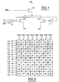
- This current bit cell includes a decoding part with a complex gate G1 and an invertor I1 in CMOS technology, employing four N-channel transistors and four P-channel transistors, and the current bit cell proper comprising a current source P1 and two switches P2 and P3, formed by three P-channel transistors, which makes eleven transistors in total.
- a network can be produced as an array of Y rows and X columns, and the decoding scheme represented in Figure 2 is then as follows.
- All the current bit cells of a single row are connected to the same row-decoding signal L and to a full row-decoding signal Lc, while all the rows of current bits in a single column are connected to a column decoding signal Bit.
- a current bit cell such as the one in Figure 1 is defined as active when the current flows through the output S1.
- This network is organised in the form of a network of Y rows and X columns.
- the numbering of its cells from 0 to 63 expresses their order of command according to a sequence in which the commanding of a cell, such that the cell No. 0 located in a quadrant I of the network is followed by the commanding of a cell such as the cell No. 1 located in a quadrant III which is symmetrical to the previous quadrant with respect to the centre of the network manifested by the intersection of the lines V and H separating the network into four quadrants.
- the digital signals Bit 0 to Bit 7 are applied in turn to cells located on either side of the vertical line V separating the network into two superposed equal parts.
- the cell status signals L and the row status signals Lc are applied in turn to cells located on either side of the horizontal line H separating the network into two juxtaposed equal parts.
- the signals S1 of all the current bit cells are connected together, and the signals S2 of all the current bit cells are connected together. This leads to provision at the output S2 of the complement of the current at the output S1 with respect to the total current flowing in the network.
- the network will be referred to as unipolar.
- differential the network
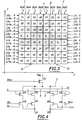
- the proposed solution is represented in Figure 4.
- the proposed current bit cell comprises a current source P1 and a set of eight switches P2 to P9 controlled by logic bit signals Bit, Bitz, L, Lz, Lc and Lcz.
- the suffix z indicates the complement.
- the signal Bitz is the complement of the signal Bit.
- the current source may use more than one transistor in the case of a current source produced in cascode in order to improve the precision of the current.
- the current bit cell represented in Figure 4 includes a current source P1 formed by a P-channel transistor whose source is connected to a voltage Vdd, whose gate receives a Bias signal and whose drain is connected to a line connecting the sources of four P-channel transistors P2, P3, P4 and P5.
- the gates of the transistors P2 and P5 are connected to an L signal line 3.
- the gate of the transistor P6 receives the signal Bit
- the gate of the transistor P7 receives the signal Lc
- the gate of the transistor P8 receives the signal Lcz
- the gate of the transistor P9 receives the signal Bitz.
- the drains of the transistors P6 and P7 are connected to a common output terminal S1, whereas the drains of the transistors P8 and P9 are connected to a common output terminal S2.
- the current bit cells in which the current is switched to the output S1 will be defined as being active.
- This current bit cell allows the same decoding scheme as the cell in Figure 1, that is to say that each individual cell can be activated, when the signals Bit are active, by means of the transistors P2 and P6, while the current bit cells of each entire row can be activated, when the signal Lc is active, by means of the transistors P3 and P7.
- the current is diverted to the output S2 when the signals Bit and L are inactive or when the entire row is inactive (Lc inactive).
- the second advantage of the arrangement of the invention resides in the fact that this structure is symmetrical from a topological point of view and symmetrical from an electrical point of view with respect to the source, on condition that the command signals Bit, L and Lc are symmetrical (no delay and the same transition time) with regard to their respective complements Bitz, Lz and Lcz.
- This symmetry of the command signals can be obtained with ease by using suitable circuits.
- a first source of error results from the following phenomenon.
- the current originating from the source is switched to the output S1
- the command signal L is inactive
- the transistor P2 is inactive
- the signal Bit is toggled as a function of the decoding of the current bit cells of the row which is active or being filled.
- the coupling between the common node of the transistors P2 and P6 and the signal Bit leads to a stray charge on the capacitor C1 when the transistor P6 is switched off.
- the command signal L is active (Lz is inactive) and the command signal Lc is inactive. This leads to the transistors P3 and P7 being switched off and makes the node common to P3 and P7 floating.
- the circuit includes a current source consisting of the P-channel transistor P1, the source of which is connected to a voltage Vdd, the gate of which receives the signal Bias and the drain of which is connected to a line 5 connecting the sources of transistor P6, the gate of which is connected to the signal Bit, of the transistor P4, the gate of which is connected to the signal Lz, and of the transistor P9, the gate of which receives the signal Bitz.
- the drain-source path of the P-channel transistor P3, the gate of which also receives the signal Lz, is connected between the drains of the transistors P6 and P9.
- the drain of the transistor P6 is connected to the source of the transistor P2
- the drain of the transistor P4 is connected to the source of the transistor P7 and to the source of the transistor P8, and the drain of the transistor P9 is connected to the source of the transistor P5.
- the gates of the transistors P2 and P5 receive the signal L, while the gate of the transistor P7 receives the signal Lc and the gate of the transistor P8 receives the signal Lcz.
- This structure avoids a node being left floating for any decoding status of the current bit cell.
- the position of the switches controlled by the signals Bit in the case of the transistor P6, and L in the case of the transistor P2 have been exchanged and the switch P3 has been placed between the common node of the transistors P2, P6 and P5, P9.
- the signal L when the signal L is inactive, there is a path from the common node of P2, P6 and P5, P9 to S1 or S2, avoiding a floating status on the node P2, P6 or P5, P9.
- the switches P7 and P8 respectively controlled by the signals Lc and Lcz are connected to a single switch P2, controlled by the signal Lz.
- This novel structure also uses only nine transistors, all of the same type, and conserves a topological and electrical symmetry.
Landscapes
- Physics & Mathematics (AREA)
- Nonlinear Science (AREA)
- Analogue/Digital Conversion (AREA)
- Electronic Switches (AREA)
Priority Applications (1)
| Application Number | Priority Date | Filing Date | Title |
|---|---|---|---|
| US09/189,073 US6160507A (en) | 1996-05-13 | 1998-11-09 | Current bit cell and switched current network formed of such cells |
Applications Claiming Priority (2)
| Application Number | Priority Date | Filing Date | Title |
|---|---|---|---|
| FR9605921 | 1996-05-13 | ||
| FR9605921A FR2748617B1 (fr) | 1996-05-13 | 1996-05-13 | Cellule de bit de courant et reseau a courant commute forme de telles cellules |
Publications (2)
| Publication Number | Publication Date |
|---|---|
| EP0808023A1 true EP0808023A1 (de) | 1997-11-19 |
| EP0808023B1 EP0808023B1 (de) | 2005-07-20 |
Family
ID=9492072
Family Applications (1)
| Application Number | Title | Priority Date | Filing Date |
|---|---|---|---|
| EP19970401063 Expired - Lifetime EP0808023B1 (de) | 1996-05-13 | 1997-05-13 | Strombitzelle und stromgeschaltetes Netzwerk mit derartigen Zellen |
Country Status (4)
| Country | Link |
|---|---|
| EP (1) | EP0808023B1 (de) |
| JP (1) | JPH1098386A (de) |
| DE (1) | DE69733732T2 (de) |
| FR (1) | FR2748617B1 (de) |
Citations (2)
| Publication number | Priority date | Publication date | Assignee | Title |
|---|---|---|---|---|
| EP0136229A2 (de) * | 1983-09-17 | 1985-04-03 | Fujitsu Limited | Leseverstärker |
| US5361233A (en) * | 1990-05-25 | 1994-11-01 | Matsushita Electric Industrial Co., Ltd. | Semiconductor memory apparatus |
-
1996
- 1996-05-13 FR FR9605921A patent/FR2748617B1/fr not_active Expired - Fee Related
-
1997
- 1997-05-13 JP JP12243597A patent/JPH1098386A/ja not_active Ceased
- 1997-05-13 EP EP19970401063 patent/EP0808023B1/de not_active Expired - Lifetime
- 1997-05-13 DE DE69733732T patent/DE69733732T2/de not_active Expired - Fee Related
Patent Citations (2)
| Publication number | Priority date | Publication date | Assignee | Title |
|---|---|---|---|---|
| EP0136229A2 (de) * | 1983-09-17 | 1985-04-03 | Fujitsu Limited | Leseverstärker |
| US5361233A (en) * | 1990-05-25 | 1994-11-01 | Matsushita Electric Industrial Co., Ltd. | Semiconductor memory apparatus |
Non-Patent Citations (1)
| Title |
|---|
| "COMBINED SENSE DECODER AND AMPLIFIER", IBM TECHNICAL DISCLOSURE BULLETIN, vol. 34, no. 10A, 1 March 1992 (1992-03-01), NEW YORK,US, pages 184 - 185, XP000302269 * |
Also Published As
| Publication number | Publication date |
|---|---|
| DE69733732T2 (de) | 2006-04-20 |
| DE69733732D1 (de) | 2005-08-25 |
| EP0808023B1 (de) | 2005-07-20 |
| JPH1098386A (ja) | 1998-04-14 |
| FR2748617B1 (fr) | 1998-08-14 |
| FR2748617A1 (fr) | 1997-11-14 |
Similar Documents
| Publication | Publication Date | Title |
|---|---|---|
| US5625360A (en) | Current source for reducing noise glitches generated in a digital to analog converter and method therefor | |
| US5164725A (en) | Digital to analog converter with current sources paired for canceling error sources | |
| US4667178A (en) | Digital to analog converter | |
| US5029305A (en) | Method and apparatus for error correction in thermometer code arrays | |
| US9998131B1 (en) | Hybrid analog-to-digital converter | |
| US4348658A (en) | Analog-to-digital converter using half range technique | |
| US4725813A (en) | MOS type circuit device | |
| US6160507A (en) | Current bit cell and switched current network formed of such cells | |
| US6297759B1 (en) | Digital-to-analog converter with high-speed output | |
| EP0298493B1 (de) | Analog-Digital-Umsetzer mit schrittweiser Annäherung | |
| US6954165B2 (en) | Voltage segmented digital to analog converter | |
| CN102332921A (zh) | 一种适用于自动增益控制环路的逐次逼近型模数转换器 | |
| KR102926954B1 (ko) | Mac 연산 동작을 수행하는 반도체 장치 | |
| Caselli et al. | Charge sharing and charge injection A/D converters for analog in-memory computing | |
| IE900490L (en) | Integrated circuit | |
| JPH0325091B2 (de) | ||
| EP0903861B1 (de) | Verfahren zur Auswahl einer Zellenfolge in einer zweidimensionalen Matrixstruktur eines Digital-Analog-Wandlers und nach diesem Verfahren arbeitender Wandler | |
| US11722127B2 (en) | Phase interpolator and phase buffer circuit | |
| US6137309A (en) | Exclusive-or logic gate with four two-by-two complementary inputs and two complementary outputs, and frequency multiplier incorporating said gate | |
| US5467089A (en) | Capacitor array digital/analog converter with compensation array for stray capacitance | |
| JPH04358418A (ja) | 多チャンネルd/a変換器 | |
| USRE35483E (en) | Switching matrix crosspoint | |
| EP0808023B1 (de) | Strombitzelle und stromgeschaltetes Netzwerk mit derartigen Zellen | |
| US4517551A (en) | Digital to analog converter circuit | |
| US6104330A (en) | Digital to analogue and analogue to digital converters |
Legal Events
| Date | Code | Title | Description |
|---|---|---|---|
| PUAI | Public reference made under article 153(3) epc to a published international application that has entered the european phase |
Free format text: ORIGINAL CODE: 0009012 |
|
| AK | Designated contracting states |
Kind code of ref document: A1 Designated state(s): DE FR GB IT NL |
|
| 17P | Request for examination filed |
Effective date: 19980515 |
|
| 17Q | First examination report despatched |
Effective date: 20020923 |
|
| GRAP | Despatch of communication of intention to grant a patent |
Free format text: ORIGINAL CODE: EPIDOSNIGR1 |
|
| GRAS | Grant fee paid |
Free format text: ORIGINAL CODE: EPIDOSNIGR3 |
|
| GRAA | (expected) grant |
Free format text: ORIGINAL CODE: 0009210 |
|
| AK | Designated contracting states |
Kind code of ref document: B1 Designated state(s): DE FR GB IT NL |
|
| PG25 | Lapsed in a contracting state [announced via postgrant information from national office to epo] |
Ref country code: NL Free format text: LAPSE BECAUSE OF FAILURE TO SUBMIT A TRANSLATION OF THE DESCRIPTION OR TO PAY THE FEE WITHIN THE PRESCRIBED TIME-LIMIT Effective date: 20050720 Ref country code: IT Free format text: LAPSE BECAUSE OF FAILURE TO SUBMIT A TRANSLATION OF THE DESCRIPTION OR TO PAY THE FEE WITHIN THE PRE;WARNING: LAPSES OF ITALIAN PATENTS WITH EFFECTIVE DATE BEFORE 2007 MAY HAVE OCCURRED AT ANY TIME BEFORE 2007. THE CORRECT EFFECTIVE DATE MAY BE DIFFERENT FROM THE ONE RECORDED.SCRIBED TIME-LIMIT Effective date: 20050720 |
|
| REG | Reference to a national code |
Ref country code: GB Ref legal event code: FG4D |
|
| REF | Corresponds to: |
Ref document number: 69733732 Country of ref document: DE Date of ref document: 20050825 Kind code of ref document: P |
|
| NLV1 | Nl: lapsed or annulled due to failure to fulfill the requirements of art. 29p and 29m of the patents act | ||
| ET | Fr: translation filed | ||
| PLBE | No opposition filed within time limit |
Free format text: ORIGINAL CODE: 0009261 |
|
| STAA | Information on the status of an ep patent application or granted ep patent |
Free format text: STATUS: NO OPPOSITION FILED WITHIN TIME LIMIT |
|
| 26N | No opposition filed |
Effective date: 20060421 |
|
| PGFP | Annual fee paid to national office [announced via postgrant information from national office to epo] |
Ref country code: FR Payment date: 20090507 Year of fee payment: 13 Ref country code: DE Payment date: 20090529 Year of fee payment: 13 |
|
| REG | Reference to a national code |
Ref country code: FR Ref legal event code: ST Effective date: 20110131 |
|
| PG25 | Lapsed in a contracting state [announced via postgrant information from national office to epo] |
Ref country code: DE Free format text: LAPSE BECAUSE OF NON-PAYMENT OF DUE FEES Effective date: 20101201 |
|
| PG25 | Lapsed in a contracting state [announced via postgrant information from national office to epo] |
Ref country code: FR Free format text: LAPSE BECAUSE OF NON-PAYMENT OF DUE FEES Effective date: 20100531 |
|
| PGFP | Annual fee paid to national office [announced via postgrant information from national office to epo] |
Ref country code: GB Payment date: 20120426 Year of fee payment: 16 |
|
| GBPC | Gb: european patent ceased through non-payment of renewal fee |
Effective date: 20130513 |
|
| PG25 | Lapsed in a contracting state [announced via postgrant information from national office to epo] |
Ref country code: GB Free format text: LAPSE BECAUSE OF NON-PAYMENT OF DUE FEES Effective date: 20130513 |