EP0807943A1 - Batterie a couches minces et son procede et dispositif de production - Google Patents
Batterie a couches minces et son procede et dispositif de production Download PDFInfo
- Publication number
- EP0807943A1 EP0807943A1 EP96901104A EP96901104A EP0807943A1 EP 0807943 A1 EP0807943 A1 EP 0807943A1 EP 96901104 A EP96901104 A EP 96901104A EP 96901104 A EP96901104 A EP 96901104A EP 0807943 A1 EP0807943 A1 EP 0807943A1
- Authority
- EP
- European Patent Office
- Prior art keywords
- thin
- film
- dielectric
- substrate
- films
- Prior art date
- Legal status (The legal status is an assumption and is not a legal conclusion. Google has not performed a legal analysis and makes no representation as to the accuracy of the status listed.)
- Withdrawn
Links
Images



Classifications
-
- H—ELECTRICITY
- H01—ELECTRIC ELEMENTS
- H01M—PROCESSES OR MEANS, e.g. BATTERIES, FOR THE DIRECT CONVERSION OF CHEMICAL ENERGY INTO ELECTRICAL ENERGY
- H01M10/00—Secondary cells; Manufacture thereof
- H01M10/05—Accumulators with non-aqueous electrolyte
- H01M10/056—Accumulators with non-aqueous electrolyte characterised by the materials used as electrolytes, e.g. mixed inorganic/organic electrolytes
- H01M10/0561—Accumulators with non-aqueous electrolyte characterised by the materials used as electrolytes, e.g. mixed inorganic/organic electrolytes the electrolyte being constituted of inorganic materials only
- H01M10/0562—Solid materials
-
- C—CHEMISTRY; METALLURGY
- C23—COATING METALLIC MATERIAL; COATING MATERIAL WITH METALLIC MATERIAL; CHEMICAL SURFACE TREATMENT; DIFFUSION TREATMENT OF METALLIC MATERIAL; COATING BY VACUUM EVAPORATION, BY SPUTTERING, BY ION IMPLANTATION OR BY CHEMICAL VAPOUR DEPOSITION, IN GENERAL; INHIBITING CORROSION OF METALLIC MATERIAL OR INCRUSTATION IN GENERAL
- C23C—COATING METALLIC MATERIAL; COATING MATERIAL WITH METALLIC MATERIAL; SURFACE TREATMENT OF METALLIC MATERIAL BY DIFFUSION INTO THE SURFACE, BY CHEMICAL CONVERSION OR SUBSTITUTION; COATING BY VACUUM EVAPORATION, BY SPUTTERING, BY ION IMPLANTATION OR BY CHEMICAL VAPOUR DEPOSITION, IN GENERAL
- C23C14/00—Coating by vacuum evaporation, by sputtering or by ion implantation of the coating forming material
- C23C14/04—Coating on selected surface areas, e.g. using masks
- C23C14/042—Coating on selected surface areas, e.g. using masks using masks
-
- C—CHEMISTRY; METALLURGY
- C23—COATING METALLIC MATERIAL; COATING MATERIAL WITH METALLIC MATERIAL; CHEMICAL SURFACE TREATMENT; DIFFUSION TREATMENT OF METALLIC MATERIAL; COATING BY VACUUM EVAPORATION, BY SPUTTERING, BY ION IMPLANTATION OR BY CHEMICAL VAPOUR DEPOSITION, IN GENERAL; INHIBITING CORROSION OF METALLIC MATERIAL OR INCRUSTATION IN GENERAL
- C23C—COATING METALLIC MATERIAL; COATING MATERIAL WITH METALLIC MATERIAL; SURFACE TREATMENT OF METALLIC MATERIAL BY DIFFUSION INTO THE SURFACE, BY CHEMICAL CONVERSION OR SUBSTITUTION; COATING BY VACUUM EVAPORATION, BY SPUTTERING, BY ION IMPLANTATION OR BY CHEMICAL VAPOUR DEPOSITION, IN GENERAL
- C23C14/00—Coating by vacuum evaporation, by sputtering or by ion implantation of the coating forming material
- C23C14/22—Coating by vacuum evaporation, by sputtering or by ion implantation of the coating forming material characterised by the process of coating
- C23C14/34—Sputtering
- C23C14/3464—Sputtering using more than one target
-
- C—CHEMISTRY; METALLURGY
- C23—COATING METALLIC MATERIAL; COATING MATERIAL WITH METALLIC MATERIAL; CHEMICAL SURFACE TREATMENT; DIFFUSION TREATMENT OF METALLIC MATERIAL; COATING BY VACUUM EVAPORATION, BY SPUTTERING, BY ION IMPLANTATION OR BY CHEMICAL VAPOUR DEPOSITION, IN GENERAL; INHIBITING CORROSION OF METALLIC MATERIAL OR INCRUSTATION IN GENERAL
- C23C—COATING METALLIC MATERIAL; COATING MATERIAL WITH METALLIC MATERIAL; SURFACE TREATMENT OF METALLIC MATERIAL BY DIFFUSION INTO THE SURFACE, BY CHEMICAL CONVERSION OR SUBSTITUTION; COATING BY VACUUM EVAPORATION, BY SPUTTERING, BY ION IMPLANTATION OR BY CHEMICAL VAPOUR DEPOSITION, IN GENERAL
- C23C14/00—Coating by vacuum evaporation, by sputtering or by ion implantation of the coating forming material
- C23C14/22—Coating by vacuum evaporation, by sputtering or by ion implantation of the coating forming material characterised by the process of coating
- C23C14/50—Substrate holders
- C23C14/505—Substrate holders for rotation of the substrates
-
- H—ELECTRICITY
- H01—ELECTRIC ELEMENTS
- H01G—CAPACITORS; CAPACITORS, RECTIFIERS, DETECTORS, SWITCHING DEVICES, LIGHT-SENSITIVE OR TEMPERATURE-SENSITIVE DEVICES OF THE ELECTROLYTIC TYPE
- H01G4/00—Fixed capacitors; Processes of their manufacture
- H01G4/002—Details
- H01G4/018—Dielectrics
- H01G4/06—Solid dielectrics
-
- H—ELECTRICITY
- H01—ELECTRIC ELEMENTS
- H01M—PROCESSES OR MEANS, e.g. BATTERIES, FOR THE DIRECT CONVERSION OF CHEMICAL ENERGY INTO ELECTRICAL ENERGY
- H01M14/00—Electrochemical current or voltage generators not provided for in groups H01M6/00 - H01M12/00; Manufacture thereof
-
- H—ELECTRICITY
- H01—ELECTRIC ELEMENTS
- H01M—PROCESSES OR MEANS, e.g. BATTERIES, FOR THE DIRECT CONVERSION OF CHEMICAL ENERGY INTO ELECTRICAL ENERGY
- H01M6/00—Primary cells; Manufacture thereof
- H01M6/40—Printed batteries, e.g. thin film batteries
-
- H—ELECTRICITY
- H01—ELECTRIC ELEMENTS
- H01M—PROCESSES OR MEANS, e.g. BATTERIES, FOR THE DIRECT CONVERSION OF CHEMICAL ENERGY INTO ELECTRICAL ENERGY
- H01M10/00—Secondary cells; Manufacture thereof
- H01M10/04—Construction or manufacture in general
- H01M10/0431—Cells with wound or folded electrodes
-
- H—ELECTRICITY
- H01—ELECTRIC ELEMENTS
- H01M—PROCESSES OR MEANS, e.g. BATTERIES, FOR THE DIRECT CONVERSION OF CHEMICAL ENERGY INTO ELECTRICAL ENERGY
- H01M10/00—Secondary cells; Manufacture thereof
- H01M10/04—Construction or manufacture in general
- H01M10/0436—Small-sized flat cells or batteries for portable equipment
-
- H—ELECTRICITY
- H01—ELECTRIC ELEMENTS
- H01M—PROCESSES OR MEANS, e.g. BATTERIES, FOR THE DIRECT CONVERSION OF CHEMICAL ENERGY INTO ELECTRICAL ENERGY
- H01M10/00—Secondary cells; Manufacture thereof
- H01M10/05—Accumulators with non-aqueous electrolyte
- H01M10/058—Construction or manufacture
- H01M10/0585—Construction or manufacture of accumulators having only flat construction elements, i.e. flat positive electrodes, flat negative electrodes and flat separators
-
- H—ELECTRICITY
- H01—ELECTRIC ELEMENTS
- H01M—PROCESSES OR MEANS, e.g. BATTERIES, FOR THE DIRECT CONVERSION OF CHEMICAL ENERGY INTO ELECTRICAL ENERGY
- H01M10/00—Secondary cells; Manufacture thereof
- H01M10/05—Accumulators with non-aqueous electrolyte
- H01M10/058—Construction or manufacture
- H01M10/0587—Construction or manufacture of accumulators having only wound construction elements, i.e. wound positive electrodes, wound negative electrodes and wound separators
-
- H—ELECTRICITY
- H01—ELECTRIC ELEMENTS
- H01M—PROCESSES OR MEANS, e.g. BATTERIES, FOR THE DIRECT CONVERSION OF CHEMICAL ENERGY INTO ELECTRICAL ENERGY
- H01M2220/00—Batteries for particular applications
- H01M2220/20—Batteries in motive systems, e.g. vehicle, ship, plane
-
- H—ELECTRICITY
- H01—ELECTRIC ELEMENTS
- H01M—PROCESSES OR MEANS, e.g. BATTERIES, FOR THE DIRECT CONVERSION OF CHEMICAL ENERGY INTO ELECTRICAL ENERGY
- H01M6/00—Primary cells; Manufacture thereof
- H01M6/04—Cells with aqueous electrolyte
- H01M6/06—Dry cells, i.e. cells wherein the electrolyte is rendered non-fluid
- H01M6/10—Dry cells, i.e. cells wherein the electrolyte is rendered non-fluid with wound or folded electrodes
-
- H—ELECTRICITY
- H01—ELECTRIC ELEMENTS
- H01M—PROCESSES OR MEANS, e.g. BATTERIES, FOR THE DIRECT CONVERSION OF CHEMICAL ENERGY INTO ELECTRICAL ENERGY
- H01M6/00—Primary cells; Manufacture thereof
- H01M6/14—Cells with non-aqueous electrolyte
- H01M6/18—Cells with non-aqueous electrolyte with solid electrolyte
- H01M6/188—Processes of manufacture
-
- Y—GENERAL TAGGING OF NEW TECHNOLOGICAL DEVELOPMENTS; GENERAL TAGGING OF CROSS-SECTIONAL TECHNOLOGIES SPANNING OVER SEVERAL SECTIONS OF THE IPC; TECHNICAL SUBJECTS COVERED BY FORMER USPC CROSS-REFERENCE ART COLLECTIONS [XRACs] AND DIGESTS
- Y02—TECHNOLOGIES OR APPLICATIONS FOR MITIGATION OR ADAPTATION AGAINST CLIMATE CHANGE
- Y02E—REDUCTION OF GREENHOUSE GAS [GHG] EMISSIONS, RELATED TO ENERGY GENERATION, TRANSMISSION OR DISTRIBUTION
- Y02E60/00—Enabling technologies; Technologies with a potential or indirect contribution to GHG emissions mitigation
- Y02E60/10—Energy storage using batteries
-
- Y—GENERAL TAGGING OF NEW TECHNOLOGICAL DEVELOPMENTS; GENERAL TAGGING OF CROSS-SECTIONAL TECHNOLOGIES SPANNING OVER SEVERAL SECTIONS OF THE IPC; TECHNICAL SUBJECTS COVERED BY FORMER USPC CROSS-REFERENCE ART COLLECTIONS [XRACs] AND DIGESTS
- Y02—TECHNOLOGIES OR APPLICATIONS FOR MITIGATION OR ADAPTATION AGAINST CLIMATE CHANGE
- Y02P—CLIMATE CHANGE MITIGATION TECHNOLOGIES IN THE PRODUCTION OR PROCESSING OF GOODS
- Y02P70/00—Climate change mitigation technologies in the production process for final industrial or consumer products
- Y02P70/50—Manufacturing or production processes characterised by the final manufactured product
-
- Y—GENERAL TAGGING OF NEW TECHNOLOGICAL DEVELOPMENTS; GENERAL TAGGING OF CROSS-SECTIONAL TECHNOLOGIES SPANNING OVER SEVERAL SECTIONS OF THE IPC; TECHNICAL SUBJECTS COVERED BY FORMER USPC CROSS-REFERENCE ART COLLECTIONS [XRACs] AND DIGESTS
- Y02—TECHNOLOGIES OR APPLICATIONS FOR MITIGATION OR ADAPTATION AGAINST CLIMATE CHANGE
- Y02T—CLIMATE CHANGE MITIGATION TECHNOLOGIES RELATED TO TRANSPORTATION
- Y02T10/00—Road transport of goods or passengers
- Y02T10/60—Other road transportation technologies with climate change mitigation effect
- Y02T10/70—Energy storage systems for electromobility, e.g. batteries
Definitions
- the present invention relates to a thin-film battery and a method and device for manufacturing a thin-film battery, and more particularly to a secondary battery.
- a battery is a device that converts electrical energy to chemical energy for storage, and is composed of a combination of positive electrodes, active material/electrolyte/active material, and negative electrodes. Electron conducting materials are used for the positive and negative electrodes, ion conducting materials are used for the electrolyte, oxidation agents are used for the positive electrode active material, and reducing agents are used for the negative electrode active material.
- the solvent density is 0.7 to 1.6 g/cm 3 , and this accounts for most of the battery volume and weight. Since the energy density of current secondary batteries is thus about 42 Wh/kg, a certain volume and weight is needed for the energy that is to be stored, making the volume and weight of the electrolyte a major issue in applications for electrical automobiles or solar cars. For example, when energy corresponding to 40 L of gasoline is stored, the fuel cell has a volume of 200 L and a weight of 400 kg, and must therefore occupy the rear seat or luggage compartment.
- an object of the present invention is to provide a compact, light-weight battery with dramatically higher energy density.
- the first of the present inventions is a thin-film battery in which dielectric thin films are interposed between conductive films serving as electrodes to store electrical energy, characterized by comprising dielectric thin films having a thickness established by the following formula E ⁇ d 2n-1 where E is the electrical energy that can be stored, d is the thickness of the dielectric thin films, and the exponent n is no more than 0.5.
- a Ba 0.5 Sr 0.5 TiO 3 thin film or the like is preferably used for the dielectric thin films.
- the dielectric thin film referred to here indicates one having the property of storing an electric charge when an electrical field is applied.
- dielectric thin films include Ba 0.5 Sr 0.5 TiO 3 , SrTiO 3 , and MgNbO 3 , as well as Pb 0.99 Nb 0.02 ((Zn 0.8 Sn 0.4 ) 0.94 Ti 0.06 ) 0.98 O 3 , Pb 0.97 La 0.02 Zr 0.66 Sn 0.24 Ti 0.10 O 3 , and other such antiferroelectric thin films.
- the dielectric thin film is preferably characterized by comprising a multilayered structure of two or more laminated layers.
- the thin-film battery is even more preferably characterized by comprising a multilayered structure of two or more layers laminated on the surface of a flat substrate.
- the second of the present inventions is characterized by comprising: a cylindrical or columnar substrate; a four-layered laminate structure consisting of a first thin-film electrode, a first dielectric thin film, a second thin-film electrode, and a second dielectric thin film, spirally wound around the surface of the substrate; and first and second output electrodes attached to the first and second thin-film electrodes.
- the substrate is preferably characterized by comprising a lanthanum strontium gallate (LaSrGaO 4 ) monocrystalline substrate.
- LaSrGaO 4 lanthanum strontium gallate
- the first and/or second thin-film electrode(s) are/is preferably characterized by comprising any of Bi 2 Sr 2 O 6-x (0 ⁇ x ⁇ 0.5), Ca 1-x Sr x RuO 3 (0.4 ⁇ x ⁇ 0.6), SrCrO 3 , Er 1-x Nb x O 3 (0 ⁇ x ⁇ 0.3), BaPbO 3 , YBa 2 Cu 3 O 7 , Nd 2-x Sr x CuO 4 (0.1 ⁇ x ⁇ 0.5), La 2-x Sr x CuO 4 (0.1 ⁇ x ⁇ 0.5), and Nb x Sr 1-x TiO 3 (0.0001 ⁇ x ⁇ 0.001).
- Ba 0.5 Sr 0.5 TiO 3 thin films, SrTiO 3 , and MgNbO 3 , as well as Pb 0.99 Nb 0.02 ((Zn 0.8 Sn 0.4 ) 0.94 Ti 0.06 ) 0.98 O 3 , Pb 0.97 La 0.02 Zr 0.66 Sn 0.24 Ti 0.10 O 3 , and other such antiferroelectric thin films are effective as dielectric thin films.
- the third of the present inventions is a method for manufacturing a thin-film battery, comprising the steps of: a battery-forming step for forming a thin-film battery by sequentially establishing at least first through fourth positions at prescribed intervals along the outer periphery of a cylindrical or columnar substrate as the substrate is rotated, so as to form a first thin-film electrode in the first position, a first dielectric thin film in the second position in the region where the first thin-film electrode has been formed, a second thin-film electrode in the third position in the region where the first dielectric thin film has been formed, and a second dielectric thin film in the fourth position in the region where the second thin-film electrode has been formed, these steps being such that the films are first formed sequentially at prescribed intervals of time and are subsequently continuously formed simultaneously, so that a four-layered laminate structure consisting of the first thin-film electrode, the first dielectric thin film, the second thin-film electrode, and the second dielectric thin film is spirally wound around the surface of the substrate; and an output electrode-forming step
- the fourth of the present inventions is characterized by comprising a vacuum vessel equipped with: a substrate support platform for rotatably supporting a cylindrical or columnar substrate; a cylindrical mask that has at least four slits formed parallel to the rotating shaft, and that is set up at a prescribed distance from the surface of the substrate; four targets for at least a first thin-film electrode, first dielectric thin film, second thin-film electrode, and second dielectric thin film, located in prescribed regions in the vacuum vessel corresponding to the four slits; and energy supply means for supplying energy rays to the targets, wherein particle beams scattered from the targets by the energy from the energy supply means pass through the slits of the mask and reach the substrate, resulting in the sequential formation of a four-layered laminate structure consisting of a first thin-film electrode, first dielectric thin film, second thin-film electrode, and second dielectric thin film spirally wound around the surface of the substrate.
- the fifth of the present inventions is characterized in that the thickness d of the dielectric thin films is established so as to be no more than 3 times a critical thickness d c at which the dielectric constant is proportional to the thickness, and the thin-film battery has a laminated structure of at least 100 laminated layers.
- Ba 0.5 Sr 0.5 TiO 3 thin films, SrTiO 3 , and MgNbO 3 , as well as Pb 0.99 Nb 0.02 ((Zn 0.8 Sn 0.4 ) 0.94 Ti 0.06 ) 0.98 O 3 , Pb 0.97 La 0.02 Zr 0.66 Sn 0.24 Ti 0.10 O 3 , and other such antiferroelectric thin films are effective as dielectric thin films.
- the voltage applied to the capacitor can be increased because the dielectric breakdown voltage increases considerably when a capacitor is formed in this thickness region.
- the critical thickness d c differs depending on the material.
- A is a material constant.
- the maximum electrical field applied to the dielectric is given by the dielectric breakdown strength F max , except in the submicron thin film region.
- F max B ⁇ d (n-1)
- E(CGS)/gr (1/(2 ⁇ 9 ⁇ 10 11 ))( ⁇ r (bulk) ⁇ 0 (B 2 )(1/2 ⁇ )d 2n-2 )) d ⁇ d c
- E(CGS)/gr (1/(2 ⁇ 9 ⁇ 10 11 ))( ⁇ r (bulk) ⁇ 0 (B 2 )(1/2 ⁇ )d 2n-2 )) d ⁇ d c
- E(CGS)/gr (1/(2 ⁇ 9 ⁇ 10 11 ))( ⁇ r (bulk) ⁇ 0 (B 2 )(1/2 ⁇ )d 2n-2 )) d ⁇ d c
- ⁇ is the average density of the dielectrics and electrodes.
- the dielectric constant of the dielectric is entirely the same as in Formula (3), but the dielectric breakdown strength F max begins to increase rapidly with decreases in the thickness of the thin film. This is also expressed by the exponential function of the thickness, but the exponent is different than that in Formula (4).
- F max B' ⁇ d n'-1
- the exponent n'-1 is usually negative.
- the dielectric breakdown voltage (V max ) is obtained by multiplying the film thickness.
- V max B' ⁇ d n'
- the exponent n' is also negative.
- E(CGS)/gr (1/2 ⁇ 9 ⁇ 10 11 ))( ⁇ 0 A(B ⁇ 2 )(1/2 ⁇ ) ⁇ d 2n-1 )) d ⁇ d c
- the dielectric breakdown voltage is exponentially dependent on the thickness of the dielectric, and this exponent should essentially be no more than 0.5, in order to increase the energy density of a thin-film capacitor.
- d ⁇ d c the maximum stored energy density of a capacitor is increased simply by lowering the film thickness, but when d ⁇ d c , depending on the selection of the exponent n, lowering the film thickness sometimes does not result in an increase in stored energy density, so the selection of the exponent n (the selection of a material having the exponent n) is important in order to increase the stored energy density with a compact size.
- the thinner the dielectric thickness the greater the energy density. Since a reduction in the dielectric thickness also results in a lower capacitor volume, even laminated structures of 100 layers or more allow the energy that is stored to be dramatically increased without increasing the size. However, since the dielectric breakdown voltage decreases dramatically depending on the dielectric grain boundary and the like, it is important to enhance the performance by the heteroepitaxial formation of the dielectric thin films and thin-film electrodes.
- tunnel current can no longer be disregarded as the dielectric thickness decreases, so tunnel current should be reduced by minimizing the overlap of wave functions as a result of combinations of different types of Fermi surface wave functions governing the electric conduction of the pairs of metal or conductive oxide thin-film electrodes sandwiching the thin films of high dielectric materials.
- the dielectric thin films have a thinness that cannot be realized in ceramic capacitors, allowing multiple layers to be made with low surface area and the stored energy density to be dramatically decreased.
- the thin-film battery has a multilayered structure with two or more laminated layers, allowing the stored electrical energy to be greatly increased.
- the thickness of the dielectric thin films should be no more than 5 ⁇ m, and even more preferably between 0.1 and 1 ⁇ m.
- the critical film thickness of the various dielectric thin films is no more than 5 ⁇ m and is used at or below this film thickness.
- a large-capacity thin-film battery with a high stored energy efficiency can be obtained by laminating thin-film batteries of 100 layers or more.
- the dielectric thin film material and thickness are selected in accordance with the aforementioned conditions, and a four-layered laminate consisting of a first dielectric thin film, first thin-film electrode, second dielectric thin film, and second thin-film electrode is formed and is spirally wound around the surface of a cylindrical or columnar substrate, so as obtain an extremely compact thin-film battery with substantial stored energy.
- the substrate is preferably made of a lanthanum-strontium gallate (LaSrGaO 4 ) monocrystalline substrate, allowing the lattice constant to be made closer to that of the thin-film electrodes, allowing epitaxial growth to be achieved, and allowing the orientation to be enhanced and stored energy loss to be minimized.
- LaSrGaO 4 lanthanum-strontium gallate
- the first and/or second thin-film electrodes are preferably formed of any of Ca 1-x Sr x RuO 3 (0.4 ⁇ x ⁇ 0.6), SrCrO 3 , Er 1-x Nb x O 3 (0 ⁇ x ⁇ 0.3), BaPbO 3 , YBa 2 Cu 3 O 7 , Nd 2-x Sr x CuO 4 (0.1 ⁇ x ⁇ 0.5), La 2-x Sr x CuO 4 (0.1 ⁇ x ⁇ 0.5), and Nb x Sr 1-x TiO 3 (0.0001 ⁇ x ⁇ 0.001), allowing the lattice constant to be made closer to that of the substrate to obtain thin-film electrodes with better orientation.
- the first and second thin-film electrodes may also be made of different materials on the positive and negative electrode sides.
- multilayered films are continuously formed in sequence to form laminated films with extreme ease in spiral form.
- the thickness of each layer can be regulated with extreme ease by regulating the rotating speed of the substrate support platform and the amount of energy supplied, allowing large-capacity thin-film batteries to be formed.
- a large-capacity thin-film battery can be formed using dielectric thin films having a thickness no more than 3 times the critical film thickness.
- An externally attached circuit is needed to extract current at a fixed voltage in thin-film batteries in which Ba 0.5 Sr 0.5 TiO 3 , MgNbO 3 , or the like is used as the dielectric thin film, but since it is possible to extract a charge only at a constant voltage with antiferroelectric thin films, the voltage is necessarily constant, making such a circuit unnecessary when batteries are manufactured using antiferroelectric thin films.
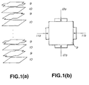
- the thin-film battery is made by alternately laminating 10 6 times 0.1 ⁇ m thick Nd 1.5 Ce 0.5 CuO 4 thin films as thin-film electrodes 9 and 0.1 ⁇ m thick Ba 0.5 Sr 0.5 TiO 3 thin films 10 as the dielectric thin films on the surface of a strontium titanate (SrTiO 3 ) substrate 8, wherein the uppermost layer is used as a thin-film electrode 9, an electrical connection is made through output electrodes 11a and 12a, and the batteries are connected in series.
- a strontium titanate (SrTiO 3 ) substrate 8 wherein the uppermost layer is used as a thin-film electrode 9, an electrical connection is made through output electrodes 11a and 12a, and the batteries are connected in series.
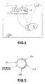
- a substrate holder 2 equipped with a heater is formed in a vacuum chamber 1 as shown in Fig. 2, and a device that is equipped with a mask exchange mechanism 3 with two types of masks for forming dielectric thin films and thin-film electrodes, a first target 4 consisting of the dielectric material and a second target 5 consisting of the electrode material, and an oxygen plasma gun 6 for radiating oxygen plasma onto the substrate 8 to be treated on the substrate holder 2 is used.
- a transmitting window 7 though which ultraviolet rays are transmitted is formed in the vacuum chamber 1, and light is guided from an ultraviolet ray laser on the outside of the vacuum chamber 1 onto the targets.
- a movable mirror is used to adjust the laser light so that it selectively reached the targets 4 and 5 in sequence.
- the laser light is 1 J/cm 2
- the repeating frequency is 10 Hz
- the substrate holder temperature is 700°C.
- the 1.6 cm long ⁇ 6.5 cm wide strontium titanate (SrTiO 3 ) substrate 8 is placed on the substrate holder 2 of the device, a mask for forming a thin-film electrode is selected by the mask exchange mechanism 3, and laser light is radiated onto the first target 4. At this time, clusters, ions, molecules, and electrons are scattered from the target surface, resulting in the formation of an Nd 1.5 Ce 0. Cu 5 O 4 thin film as a thin-film electrode 9.
- Oxygen plasma oxygen flow rate of 0.1 L/min, high frequency power of 50 W
- This process results in a centerline mean roughness Ra of 0.5 nm.
- a mask for forming a dielectric thin film is then selected by the mask exchange mechanism 3, and laser light is radiated onto the second target 5.
- a 0.1 ⁇ m thick Ba 0.5 Sr 0.5 TiO 3 thin film is thus formed as a dielectric thin film 10, and oxygen plasma (oxygen flow rate of 0.1 L/min, high frequency power of 50 W) is again irradiated to smooth the surface of the dielectric thin film 10. This process results in a centerline mean roughness Ra of 0.5 nm.
- a 1.6 cm long ⁇ 6.5 cm wide battery manufactured by laminating 3 ⁇ 10 4 layers of dielectric layers according to the same method has a volume of 1.6 cm ⁇ 6.5 cm ⁇ 0.6 cm and stored energy of 570 Wh when charged with 100 V, which is about 800 times the energy that is stored in conventional Ni-Cd batteries of the same size when charged with 1.2 V.
- a laminated type of structure was given in the foregoing example, but the invention can also be adapted to thin-film batteries having single-layer structures, and since this is an extremely thin type of battery, a thin-film electrode, dielectric thin film, and thin-film electrode can be laminated via a buffer layer and integrated with the reverse side of a movable terminal.
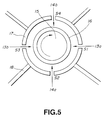
- this thin-film battery is made by spirally forming a four-layered laminate consisting of a 0.1 ⁇ m thick Nb x Sr 1-x TiO 3 thin film electrode 21a, a 0.1 ⁇ m thick Ba 0.5 Sr 0.5 TiO 3 dielectric thin film 22a, a 0.1 ⁇ m thick Nb x Sr 1-x TiO 3 thin film electrode 21b, and a 0.1 ⁇ m thick Ba 0.5 Sr 0.5 TiO 3 dielectric thin film 22b around the surface of a cylindrical lanthanum-strontium gallate (LaSrGaO 4 ) substrate 16.
- LaSrGaO 4 cylindrical lanthanum-strontium gallate
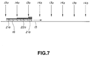
- a rotatable cylindrical substrate holder 15 equipped with a heater is located in a vacuum chamber 19 as shown in Fig. 4, a roll-shaped substrate 16 is placed on the substrate holder 15, a cylindrical mask 17 having 4 slits S is placed in a location at a prescribed distance from the surface of the substrate 16, and a device equipped with first targets 13a and 13b consisting of Nb x Sr 1-x TiO 3 (0.0001 ⁇ x ⁇ 0.001) as the electrode material and second targets 14a and 14b consisting of Ba 0.5 Sr 0.5 TiO 3 as the dielectric material and Nb x Sr 1-x TiO 3 (0.0001 ⁇ x ⁇ 0.001) as the electrode material is used.
- a transmitting window 20 though which ultraviolet rays are transmitted is formed in the vacuum chamber 19, and light is guided from an ultraviolet ray laser on the outside of the vacuum chamber 19 onto the targets.
- targets 13a, 13b, 14a, and 14b are irradiated with laser light, but the initial irradiation can be shifted in set increments of time.
- the mask 17 has slits S1 through S4 parallel to the rotating shaft in four locations, and the slit width is adjusted according to the rotating speed of the substrate holder 15. As shown in Fig.
- the first thin-film electrode and first dielectric film and the second thin-film electrode and second dielectric thin film are sequentially formed in their respective locations by the particles transmitted through the slits S1 through S4, and are thus alternately laminated continuously in spiral form around the surface of the rotating substrate.
- the laser light is 1 J/cm2
- the repeating frequency is 10 Hz
- the substrate holder temperature is 700°C.
- the cylindrical lanthanum-strontium gallate (LaSrGaO 4 ) substrate 16 is placed on the substrate holder 15 of the device, the mask 17 and barrier 18 are set up, the substrate holder 15 is then rotated at a prescribed rotating speed, and the first target 13a begins to be irradiated with laser light first. At this time, clusters, ions, molecules, or electrons are scattered from the target surface and reach the substrate surface through the slit S1, and a 0.1 ⁇ m thick Nb x Sr 1-x TiO 3 thin film begins to be formed as the thin-film electrode 21a.
- LaSrGaO 4 The cylindrical lanthanum-strontium gallate
- the second target 14a begins to be irradiated with laser light.
- a 01 ⁇ m thick Ba 0.5 Sr 0.5 TiO 3 thin film begins to be formed as the dielectric thin film 22a.
- the first target 13b begins to be irradiated with laser light.
- a 0.1 ⁇ m thick Nb x Sr 1-x TiO 3 thin film is formed as the thin-film electrode 21b.
- a 0.1 ⁇ m thick Ba 0.5 Sr 0.5 TiO 3 thin film begins to be formed as the dielectric thin film 22b.
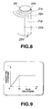
- Thin films are thus laminated in sequence by the continuing supply of clusters, atoms, or molecules from the slits (Fig. 6 is an illustration of the process; Fig. 6(a) illustrates the beginning of the process, and Fig. 6(b) illustrates the final process).
- Fig. 7 is a plan illustrating this. That is, as the substrate surface travels, each thin film is produced in successive zones. As shown in cross section Fig. 3, a four-layered laminate consisting of the thin-film electrode 21a, dielectric thin film 22a, thin-film electrode 21b, and dielectric thin film 22b is thus formed in a spiral.
- output electrodes 23a and 23b are attached to the thin-film electrodes 21a and 21b so as to complete the thin-film battery.
- the films were sequentially formed as the substrate was rotated, but the substrate may be composed of a thin insulating film; a three-layered film consisting of a thin-film electrode, dielectric thin film, and thin-film electrode may be continuously formed in sequence as the film is wound from a feed roll serving as a substrate holder onto a winding roll (a roll is formed while laminated, in the same manner as shown in Fig. 7); and a thin-film battery in the form of a spiral similar to that depicted in Fig. 3 may be obtained.
- a thin-film battery consisting of multilayered films can thus be formed with extreme ease.
- the film thickness can be readily adjusted here too by adjusting the substrate rotating speed and the energy supplied to the targets.
- Suitable materials other than those used in the foregoing examples can be used as the electrode material and dielectric thin film material.
- materials with similar lattice constants may be selected or a layer of graduated composition may be interposed to alleviate differences in lattice constant. Because the dielectric constant differs depending on the axial direction of the crystals, dielectrics may be epitaxially grown in the direction in which the dielectric constant is greater.
- the present invention allows a compact battery with high energy density to be provided.
Landscapes
- Chemical & Material Sciences (AREA)
- Engineering & Computer Science (AREA)
- Chemical Kinetics & Catalysis (AREA)
- Manufacturing & Machinery (AREA)
- Electrochemistry (AREA)
- General Chemical & Material Sciences (AREA)
- Power Engineering (AREA)
- Materials Engineering (AREA)
- Mechanical Engineering (AREA)
- Metallurgy (AREA)
- Organic Chemistry (AREA)
- Physics & Mathematics (AREA)
- General Physics & Mathematics (AREA)
- Inorganic Chemistry (AREA)
- Condensed Matter Physics & Semiconductors (AREA)
- Microelectronics & Electronic Packaging (AREA)
- Secondary Cells (AREA)
- Battery Electrode And Active Subsutance (AREA)
- Fixed Capacitors And Capacitor Manufacturing Machines (AREA)
- Ceramic Capacitors (AREA)
Applications Claiming Priority (3)
| Application Number | Priority Date | Filing Date | Title |
|---|---|---|---|
| JP7009204A JPH08203777A (ja) | 1995-01-24 | 1995-01-24 | 薄膜電池、薄膜電池の製造方法および薄膜電池製造装置 |
| JP9204/95 | 1995-01-24 | ||
| PCT/JP1996/000123 WO1996023312A1 (fr) | 1995-01-24 | 1996-01-24 | Batterie a couches minces et son procede et dispositif de production |
Publications (1)
| Publication Number | Publication Date |
|---|---|
| EP0807943A1 true EP0807943A1 (fr) | 1997-11-19 |
Family
ID=11713956
Family Applications (1)
| Application Number | Title | Priority Date | Filing Date |
|---|---|---|---|
| EP96901104A Withdrawn EP0807943A1 (fr) | 1995-01-24 | 1996-01-24 | Batterie a couches minces et son procede et dispositif de production |
Country Status (4)
| Country | Link |
|---|---|
| EP (1) | EP0807943A1 (fr) |
| JP (1) | JPH08203777A (fr) |
| KR (1) | KR960030464A (fr) |
| WO (1) | WO1996023312A1 (fr) |
Families Citing this family (2)
| Publication number | Priority date | Publication date | Assignee | Title |
|---|---|---|---|---|
| JP3705567B2 (ja) * | 1999-02-19 | 2005-10-12 | 松下電器産業株式会社 | 薄膜の製造方法及び製造装置並びに薄膜及び薄膜積層体及び薄膜部品 |
| US20100252419A1 (en) * | 2009-02-02 | 2010-10-07 | Klaus Bollmann | Method of manufacturing a high density capacitor or other microscopic layered mechanical device |
Family Cites Families (4)
| Publication number | Priority date | Publication date | Assignee | Title |
|---|---|---|---|---|
| DE2843581C2 (de) * | 1978-10-05 | 1986-03-27 | Siemens AG, 1000 Berlin und 8000 München | Elektrischer Schichtkondensator und Verfahren zu seiner Herstellung |
| EP0339844A3 (fr) * | 1988-04-29 | 1991-01-16 | SPECTRUM CONTROL, INC. (a Delaware corporation) | Structure multicouche et son procédé de fabrication |
| JPH05166666A (ja) * | 1991-12-19 | 1993-07-02 | Toshiba Corp | 金属−セラミック積層フィルム |
| JP3131498B2 (ja) * | 1992-05-22 | 2001-01-31 | 株式会社東芝 | 薄膜コンデンサ |
-
1995
- 1995-01-24 JP JP7009204A patent/JPH08203777A/ja active Pending
-
1996
- 1996-01-19 KR KR1019960001145A patent/KR960030464A/ko not_active Ceased
- 1996-01-24 EP EP96901104A patent/EP0807943A1/fr not_active Withdrawn
- 1996-01-24 WO PCT/JP1996/000123 patent/WO1996023312A1/fr not_active Ceased
Non-Patent Citations (1)
| Title |
|---|
| See references of WO9623312A1 * |
Also Published As
| Publication number | Publication date |
|---|---|
| WO1996023312A1 (fr) | 1996-08-01 |
| JPH08203777A (ja) | 1996-08-09 |
| KR960030464A (ko) | 1996-08-17 |
Similar Documents
| Publication | Publication Date | Title |
|---|---|---|
| EP2288740B1 (fr) | Fabrication en grands volumes de cellules électrochimiques en employant le dépôt physique en phase gazeuse | |
| KR100814591B1 (ko) | 리튬이온 2차전지용 음극 및 그것을 이용한 리튬이온2차전지 | |
| US6242129B1 (en) | Thin lithium film battery | |
| US20070121274A1 (en) | Small volume thin film and high energy density crystal capacitors | |
| EP2620962A1 (fr) | Dispositifs de stockage d'énergie à l'état solide | |
| US9728812B2 (en) | Electrostatic energy storage device and preparation method thereof | |
| JP6603688B2 (ja) | 高エネルギー密度蓄電装置 | |
| EP0807943A1 (fr) | Batterie a couches minces et son procede et dispositif de production | |
| JP7738278B2 (ja) | キャパシタ、電気回路、回路基板、電子機器、及び蓄電デバイス | |
| CN110720132B (zh) | 超级电容器 | |
| EP4654302A1 (fr) | Substrat composite, ensemble électrode l'utilisant et procédé de fabrication de l'ensemble électrode | |
| KR101558287B1 (ko) | 커패시터용 유전체 필름 및 이를 이용한 고에너지밀도 커패시터 제조 방법 | |
| CN101578674A (zh) | 蓄电池 | |
| RU2646531C1 (ru) | Суперконденсаторная ячейка | |
| JP4947752B2 (ja) | 蓄電体 | |
| Goldner | Attaining a solar energy economy with active thin film structures | |
| HK1156369A (en) | High volume manufacture of electrochecmicals cells using physical vapor deposition | |
| CN111542938A (zh) | 蓄电装置 | |
| Shear | Thin Film Bi-based Perovskites for High Energy Density Capacitor Applications |
Legal Events
| Date | Code | Title | Description |
|---|---|---|---|
| PUAI | Public reference made under article 153(3) epc to a published international application that has entered the european phase |
Free format text: ORIGINAL CODE: 0009012 |
|
| AK | Designated contracting states |
Kind code of ref document: A1 Designated state(s): DE NL |
|
| 17P | Request for examination filed |
Effective date: 19970725 |
|
| STAA | Information on the status of an ep patent application or granted ep patent |
Free format text: STATUS: THE APPLICATION IS DEEMED TO BE WITHDRAWN |
|
| 18D | Application deemed to be withdrawn |
Effective date: 19990803 |