EP0807886A2 - Optische Netzwerkvorrichtung - Google Patents
Optische Netzwerkvorrichtung Download PDFInfo
- Publication number
- EP0807886A2 EP0807886A2 EP97250156A EP97250156A EP0807886A2 EP 0807886 A2 EP0807886 A2 EP 0807886A2 EP 97250156 A EP97250156 A EP 97250156A EP 97250156 A EP97250156 A EP 97250156A EP 0807886 A2 EP0807886 A2 EP 0807886A2
- Authority
- EP
- European Patent Office
- Prior art keywords
- optical
- control circuit
- optical switch
- network interface
- transmission
- Prior art date
- Legal status (The legal status is an assumption and is not a legal conclusion. Google has not performed a legal analysis and makes no representation as to the accuracy of the status listed.)
- Withdrawn
Links
Images


Classifications
-
- H—ELECTRICITY
- H04—ELECTRIC COMMUNICATION TECHNIQUE
- H04Q—SELECTING
- H04Q11/00—Selecting arrangements for multiplex systems
- H04Q11/0001—Selecting arrangements for multiplex systems using optical switching
Definitions
- This invention relates to an optical network device, and more particularly to, an optical network device for connecting processors in a multiprocessor system.
- Fibre Channel which is a typical optical interconnection standard for computers and an electrical switch called Fabric is described in ANSI X3T11, Fibre Channel Physical and Signaling Interface(FC-PH), Rev 4.3 (1994), pp.19-20.
- a conventional optical network device comprises a large number network interface devices connected to processors and a switch device.
- the network interface includes a network interface control circuit, an optical transmitter, an optical receiver and a FIFO(first-in first-out) queue.
- the switch device includes an optical receiver, FIFO queues, an electrical switch and an optical transmitter.
- Data output from the source network interface device is transmitted through the optical transmitter in the network interface device, the optical fiber, the optical receiver in the switch device, the FIFO queue, the electrical switch, the optical transmitter in the switch device, the optical fiber, the optical receiver in the network interface device and the FIFO queue, to the destination network interface device.
- the conventional optical network device it takes a very long time to transmit data through the switch device, since the opto-electric conversion, serial-to-parallel conversion and decoding are conducted on the input side of the switch device and the encoding, parallel-to-serial conversion and electro-optic conversion are conducted on the output side of the switch device. It causes an increase in latency. In case of an optical network device where error detection and correction are conducted in the switch device, the latency is further increased.
- the number of parallel signal lines after the opto-electric conversion, serial-to-parallel conversion and decoding in the switch device is increased ten to hundred times that of serial signal lines. For example, when a signal line coded with 10B8B code with a throughput of 4 Gbit/s is serial-to-parallel converted down to the frequency of 100 MHz, at which the electric circuit of the switch device can be operated, the number of parallel signal lines becomes 32. In case of another electric circuit with a lower operating frequency, the number of signal lines will be further increased.
- the switch scale of which is enlarged due to such a multistage composition causes a significant increase in latency.
- a multistage switch using a plurality of small scale switches is difficult to mount.
- the switch device since the switch device is asynchronously operated to the respective network interface devices, synchronizing process and asynchronous FIFO queues to adjust timing are needed. It therefore causes a further increase in latency.
- an optical network device for connecting plurality of processors in a multiprocessor system, comprises:
- an optical network device for connecting a plurality of processors in a multiprocessor system, comprises:
- an optical network device for connecting a plurality of processors in a multiprocessor system, comprises:
- an optical network device for connecting a plurality of processors in a multiprocessor system, comprises:
- FIGS.1 to 3 Before explaining an optical network device in the preferred embodiments, the aforementioned conventional optical network device will be explained in FIGS.1 to 3.
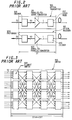
- FIG.1 shows the composition of a conventional 16 x 16 optical network device that network interface devices are interconnected by using optical interconnections and switches.
- 1100 and 1101 are network interface devices
- 1102 is a switch device
- 1110 and 1111 are network interface control circuits
- 1160 is a switch
- 1120, 1122, 1126 and 1127 are optical transmitters
- 1121, 1123, 1124 and 1125 are optical receivers
- 1130 to 1133 are FIFO(first-in first-out) queues.
- These FIFO queues also serve as asynchronous FIFO queues for absorbing the clock phase difference between the switch device and the respective network interface devices that are asynchronously operated.
- 1150 to 1153 are optical fibers and 1170 to 1172 are clock sources for the respective devices.
- FIG.2 shows typical compositions of the optical transmitter 1120 and the optical receiver 1121.
- 1210 is an encoder, where a 8B10B code is generally used.
- 1211 is a parallel-to-serial converter.
- 1212 is a laser diode, where an electro-optic conversion is conducted.
- an example of 32-bit input and 40-to-1 parallel-to-serial conversion is shown. For example, from 26.5625 MHz x 32 bit, a throughput of 1.0625(Gbit/s) can be obtained.
- 1220 is a decoder, where 10B8B decoding is conducted in response to the encoder 1210.
- 1221 is a serial-to-parallel converter.
- 1222 is a photodiode, where an opto-electric conversion is conducted.
- 32-bit input and 1-to-40 serial-to-parallel conversion in response to the optical transmitter 1120 is shown.
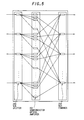
- FIG.3 shows a typical composition of the switch 1160, where sixteen 4 x 4 element switches are connected to compose a 16 x 16 switch.
- Such a switch composition is, for example, described in Proceedings of ISSP(1994), pp.396-401.
- 100 and 101 are network interface devices
- 102 is an optical switch device
- 120 and 122 are optical transmitters
- 121 and 123 are optical receivers.
- the optical transmitters and the optical receivers have the same composition as the optical transmitter 1120 and the optical receiver 1121, respectively, in FIG.1.
- 110 and 111 are network interface control circuits
- 112 is an optical switch control circuit
- 160 is an optical switch.
- 140 and 143 are transmission request signal lines
- 141 and 144 are transmission-ending signal lines
- 142 and 145 are transmission-start request signal lines.
- These are control signal lines for connecting and transmission-reception controlling between the network interface control circuits 110, 111 and the optical switch control circuit 112.
- 150 to 153 are data signal lines, which are of optical fibers.
- FIG.5 shows an example of a 16 x 16 splitter-combiner-type optical switch, where a semiconductor optical amplifier is used as a gate switch.
- 200's are sixteen 1 x 16 splitters
- 201's are two hundred and fifty six semiconductor optical amplifiers
- 202's are sixteen 16 x 1 combiner.
- an example of the optical switch that a semiconductor optical amplifier is used as a gate switch is also described in Journal of Lightwave Technologies (1992), pp.383-389.
- FIG.6A shows an example of the transmission processing of a signal.
- the network interface control circuit 110 or 111 sends out a transmission request with an addressee address to optical switch control circuit 112 through the transmission request signal line 140 or 143.
- the optical switch control circuit 112 conducts the arbitration and optical switching, then sending back a transmission-start request through the transmission-start request line 142 or 145.
- the optical switching and the sending of the transmission-start request can be parallel conducted.
- Receiving the transmission-start request the network interface control circuit 110 cr 111 starts the transmission of data.
- the network interface control circuit 110 or 111 sends the end of transmission to the optical switch control circuit 112 through the transmission-ending signal line 141 or 144.
- FIG.6C shows an example of a format of the transmitting signal. It has a frame composition composed of a bit synchronization pattern, a start bit, data and a stop bit.
- FIG.6B shows an example of the reception processing of data.
- the optical receiver conducts the bit synchronization depending on the bit synchronization pattern and detects the data position by the start bit and the stop bit.
- two clock are needed for exchanging the control signal between the network interface control circuit 110 or 111 and the optical switch control circuit 112
- five clocks are needed for the arbitration and the optical switching at the optical switch control circuit 112
- two clocks are needed as the overhead for the bit synchronization pattern and the start bit that are added to the transmitting data.
- the time required to pass a signal through the optical switch device 102 is nearly zero. Therefore, the latency becomes less than ten clocks, which is significantly lowered as compared with the 26 clocks in the conventional optical network device.
- the optical switch device 102 no opto-electric conversion and decoding are conducted and the number of signal lines are so much decreased. Moreover, by using the large-scale optical switch, the 16 x 16 switch can be obtained with the single-stage composition. Therefore, the number of interconnections, the number of element switches and the number of interconnects between the element switches can be significantly decreased or brought to zero, thereby facilitating the mounting.
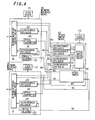
- FIG.7 An optical network device in the second preferred embodiment according to the invention, which adopts a 16 x 16 optical switch, will be explained in FIG.7.
- 400 and 401 are network interface devices
- 402 is an optical switch device
- 420 and 422 are optical transmitters
- 421 and 423 are optical receivers
- 410 and 411 are network interface control circuits
- 412 is an optical switch control circuit
- 460 is an optical switch.
- 440 and 444 are transmission request signal lines
- 441 and 445 are transmission-ending signal lines
- 442 and 446 are transmission-start request signal lines.
- These are control signal lines for connecting and transmission-reception controlling between the network interface control circuits 410, 411 and the optical switch control circuit 412.
- 450 to 453 are data signal lines, which are of optical fibers.
- 470 is a system clock source, which is distributed with identical phases through equal-length interconnections to the respective network interface devices 400, 401 and the optical switch device 402.
- the clock distribution is conducted by an electrical signal or optical signal.
- all the network control circuits composed of the network interface control circuits 410, 411 and the optical switch control circuit 412 are synchronously operated.
- 480 and 481 are re-timing circuits and 490 is a system clock in the optical switch device 402.
- FIG.8 shows an example of the re-timing circuit.
- the re-timing circuit produces a serial clock that the system clock 490 is multiplied, and the re-timing of the signal passing through the optical switch device is thereby conducted.
- shown is an example of a serial clock whose frequency is forty times that of the system clock, which is matched with the forty-to-one parallel-to-serial conversion at the optical transmitter.
- the signal After the opto-electric conversion by a photodiode 480-1, the signal is re-timed at a latching stage 480-2 composed of double latches, again electro-optic converted by a laser diode 480-3.
- the re-timing may be conducted without the opto-electric conversion.
- FIG.9 shows an example of the operation of the re-timing circuit.
- FIGS.10A to 10C show examples of the transmission processing of a signal, a format of the transmitting signal and the reception processing of data, respectively.
- the basic procedures are the same as those in the first embodiment. Since the entire system is operated synchronously, the asynchronous FIFO queue for the control signal line is not necessary. Also, due to the forced synchronization in the re-timing circuits 480, 481 of the optical switch device 402, the optical receivers 421, 423 do not need to conduct again the bit synchronization after the optical switching. Therefore, the bit synchronization is not necessary. Because of these, in the second embodiment, the latency can be further reduced as compared with that in the first embodiment.
- all the optical fibers from the optical transmitters through the optical switch to the optical receivers may have an equal length.
- the bit synchronization can be always obtained since the optical receiver receives an optical signal locked with a constant phase to the system clock.
- the line lengths of optical fibers can be equalized within a tolerance of around 1 mm, which corresponds to 5 ps skew. This value is sufficient to obtain the stable bit synchronization for up to a throughput of around 10 Gbit/s.
- FIG.11 An optical network device in the third preferred embodiment according to the invention, which adopts a 16 x 16 optical switch, will be explained in FIG.11.
- 810 and 811 are network interface control circuits
- 812 is an optical switch control circuit
- 860 is an optical switch.
- 840 and 844 are transmission request signal lines
- 841 and 845 are transmission-ending signal lines
- 842 and 846 are transmission-start request signal lines. These are control signal lines for connecting and transmission-reception controlling between the network interface control circuits 810, 811 and the optical switch control circuit 812.
- 850 to 853 are data signal lines, which are of optical fibers.
- 870 is a system clock source, which is distributed with identical phases through equal-length interconnections to network interface devices 800, 801 and an optical switch device 802.
- the clock distribution is conducted by an electrical signal or optical signal.
- the system clock all the network control circuits composed of the network interface control circuits 810, 811 and the optical switch control circuit 812 are synchronously operated.
- 880 and 881 are re-timing circuits and 890 is a system clock in the optical switch device 802.
- strobe signal lines 843 and 847 are further provided as control signal lines. Furthermore, the line length adjustment of the optical fibers for connecting between the respective network interface devices 800, 801 and the optical switch device 802 is conducted. The line lengths of the optical fibers 850, 851 are adjusted to be equal to each other and to set transmission delay time-of-flight from the parallel-to-serial converters in the optical transmitters 820, 822 to the gate switches of the optical switch 860 to be one clock.
- the line lengths of the optical fibers 852, 853 for connecting between the optical switch 860 and the respective optical receivers 821, 823 are adjusted to be equal to each other and to set the signal-passing time from the gate switches of the optical switch 860 to the serial-to-parallel in the optical receivers 821, 823 to be one clock.
- one clock corresponds to 10 ns and an optical fiber line length of 2 m.
- FIGS.12A to 12C show examples of the transmission processing of a signal, a format of the transmitting signal and the reception processing of data, respectively.
- the optical switch control circuit 812 in addition to the functions as described in the first and second embodiments, administers the transmission and reception timings of a signal in the respective network interface devices 800, 801. Signals pass through the optical switch device 802 one clock after they are transmitted from the optical transmitters 820, 822 and are received by the optical receivers 821, 823 two clocks after that. Matching with this timing, the optical switch control circuit 812 switches the optical switch 860 and notifies the optical receiver in the network interface device on the receiving side of the arrival timing of data by using the strobe signal line.
- receiving the transmission-ending signal from the network interface device on the transmitting side it notifies the optical receiver of the end of data transmission by using the strobe signal line.
- the start bit and stop bit can be eliminated.
- the data arrival timings from any optical transmitters are synchronized with the system clock, the asynchronous FIFO queues on the receiving side can be eliminated. Because of these effects, in the third embodiment, the latency can be further reduced.
- FIG.13 shows an example of a detailed timing chart in the transmission processing.
- data passes through the optical switch 860 four clocks after the optical switch control circuit 812 sends the transmission-start request back to the network interface device on the transmitting side and is received by the network interface device on the receiving side five clocks after that.
- the optical switch control circuit 812 operates the strobe signal line at the above-mentioned timings and notifies the network interface device of the validity of data.
- the network interface control circuit on the transmitting side may notify the optical switch control circuit of the length of transmitted data with the transmission request signal when requesting the transmission instead of the transmission-ending signal, and the optical switch control circuit may recognize the timing of the end of transmission by the data length and operate the strobe signal line.
- a lithium niobate matrix switch may be used.
- control signals wavelength-multiplexed with data signals may be transmitted and received between the network interface device and the optical switch device through one optical fiber.
Landscapes
- Engineering & Computer Science (AREA)
- Computer Networks & Wireless Communication (AREA)
- Data Exchanges In Wide-Area Networks (AREA)
- Optical Communication System (AREA)
- Multi Processors (AREA)
Applications Claiming Priority (3)
| Application Number | Priority Date | Filing Date | Title |
|---|---|---|---|
| JP12161396 | 1996-05-16 | ||
| JP8121613A JP2882469B2 (ja) | 1996-05-16 | 1996-05-16 | 光ネットワーク装置 |
| JP121613/96 | 1996-05-16 |
Publications (2)
| Publication Number | Publication Date |
|---|---|
| EP0807886A2 true EP0807886A2 (de) | 1997-11-19 |
| EP0807886A3 EP0807886A3 (de) | 2000-05-03 |
Family
ID=14815596
Family Applications (1)
| Application Number | Title | Priority Date | Filing Date |
|---|---|---|---|
| EP97250156A Withdrawn EP0807886A3 (de) | 1996-05-16 | 1997-05-16 | Optische Netzwerkvorrichtung |
Country Status (3)
| Country | Link |
|---|---|
| US (1) | US5905587A (de) |
| EP (1) | EP0807886A3 (de) |
| JP (1) | JP2882469B2 (de) |
Cited By (2)
| Publication number | Priority date | Publication date | Assignee | Title |
|---|---|---|---|---|
| EP1018820A3 (de) * | 1999-01-06 | 2003-01-08 | Nec Corporation | Paketvermittlungsnetz |
| EP1304901A1 (de) * | 2001-10-19 | 2003-04-23 | Alcatel | Synchronisation einer paketbasierenden Vermittlungsanlage |
Families Citing this family (14)
| Publication number | Priority date | Publication date | Assignee | Title |
|---|---|---|---|---|
| KR100295097B1 (ko) * | 1998-08-22 | 2001-08-07 | 오길록 | 광게이트를이용한광공간분할스위칭장치 |
| US7295552B1 (en) * | 1999-06-30 | 2007-11-13 | Broadcom Corporation | Cluster switching architecture |
| US6583916B2 (en) * | 1999-11-03 | 2003-06-24 | Optodot Corporation | Optical shutter assembly |
| WO2001037034A2 (en) | 1999-11-03 | 2001-05-25 | Carlson Steven A | Optical shutter |
| US6724512B2 (en) | 1999-11-03 | 2004-04-20 | Optodot Corporation | Optical switch device |
| US6751235B1 (en) * | 2000-06-27 | 2004-06-15 | Intel Corporation | Communication link synchronization method |
| US7251416B1 (en) * | 2002-05-08 | 2007-07-31 | Yotta Networks, Llc | Container based crossconnect |
| US7272309B1 (en) * | 2002-05-08 | 2007-09-18 | Yotta Networks, Llc | System and method of routing data at a photonic core |
| US7864747B2 (en) * | 2008-03-28 | 2011-01-04 | Embarq Holdings Company, Llc | System and method for communicating timing to a remote node |
| US8341628B2 (en) | 2009-12-23 | 2012-12-25 | International Business Machines Corporation | Controlling depth and latency of exit of a virtual processor's idle state in a power management environment |
| JP2012094975A (ja) * | 2010-10-25 | 2012-05-17 | Fujitsu Telecom Networks Ltd | 光パケットスイッチ装置 |
| US10735125B2 (en) | 2017-09-30 | 2020-08-04 | Juniper Networks, Inc. | Optical multicast switch with broadcast capability |
| US12323750B2 (en) | 2019-11-05 | 2025-06-03 | Mellanox Technologies, Ltd | Distributed optical circuit allocation in optical data-center networks (ODCN) |
| US11368768B2 (en) * | 2019-12-05 | 2022-06-21 | Mellanox Technologies, Ltd. | Optical network system |
Family Cites Families (2)
| Publication number | Priority date | Publication date | Assignee | Title |
|---|---|---|---|---|
| US4942574A (en) * | 1988-03-31 | 1990-07-17 | American Telephone And Telegraph Company, At&T Bell Laboratories | Concurrent resource request resolution mechanism |
| EP0794683B1 (de) * | 1991-11-29 | 2004-03-31 | Nec Corporation | Optisches ATM-Selbstlenkungsvermittlungssystem mit optischem Kopienetzwerk |
-
1996
- 1996-05-16 JP JP8121613A patent/JP2882469B2/ja not_active Expired - Fee Related
-
1997
- 1997-05-16 US US08/857,806 patent/US5905587A/en not_active Expired - Fee Related
- 1997-05-16 EP EP97250156A patent/EP0807886A3/de not_active Withdrawn
Cited By (3)
| Publication number | Priority date | Publication date | Assignee | Title |
|---|---|---|---|---|
| EP1018820A3 (de) * | 1999-01-06 | 2003-01-08 | Nec Corporation | Paketvermittlungsnetz |
| US6760346B1 (en) | 1999-01-06 | 2004-07-06 | Nec Corporation | Packet switching network |
| EP1304901A1 (de) * | 2001-10-19 | 2003-04-23 | Alcatel | Synchronisation einer paketbasierenden Vermittlungsanlage |
Also Published As
| Publication number | Publication date |
|---|---|
| US5905587A (en) | 1999-05-18 |
| JP2882469B2 (ja) | 1999-04-12 |
| EP0807886A3 (de) | 2000-05-03 |
| JPH09307562A (ja) | 1997-11-28 |
Similar Documents
| Publication | Publication Date | Title |
|---|---|---|
| US5905587A (en) | Optical network device | |
| US7672585B2 (en) | Optical switch system | |
| US6233294B1 (en) | Method and apparatus for accomplishing high bandwidth serial communication between semiconductor devices | |
| US7082546B2 (en) | Low-speed DLL employing a digital phase interpolator based upon a high-speed clock | |
| EP0311772B1 (de) | Verfahren zum Betrieb eines Koppelnetzes für optishe Busse | |
| US6674971B1 (en) | Optical communication network with receiver reserved channel | |
| US6341142B2 (en) | Serial data transceiver including elements which facilitate functional testing requiring access to only the serial data ports, and an associated test method | |
| Minkenberg et al. | Designing a crossbar scheduler for HPC applications | |
| US6578092B1 (en) | FIFO buffers receiving data from different serial links and removing unit of data from each buffer based on previous calcuations accounting for trace length differences | |
| KR101077250B1 (ko) | 광 입/출력 버스 시스템 | |
| CN101159535B (zh) | 时钟信号调节装置和方法 | |
| CN118688779A (zh) | 一种基于确定性延迟控制技术的数字阵雷达系统同步方法 | |
| US7697570B2 (en) | Method based on backboard transmitting time division multiplexing circuit data and a bridge connector | |
| US6944691B1 (en) | Architecture that converts a half-duplex bus to a full-duplex bus while keeping the bandwidth of the bus constant | |
| US7317720B2 (en) | Signal transmission system | |
| CN114050838B (zh) | 100Gbps带宽RapidIO信号源 | |
| US6081557A (en) | Datalink system and communication network | |
| US20030070033A9 (en) | Parallel and point-to-point data bus architecture | |
| KR100293430B1 (ko) | 스위칭 장비의 시스템 동기 클럭 분배 시스템 | |
| JP4023203B2 (ja) | 信号伝送システム | |
| WO2024038540A1 (en) | Switching system, optical packet transmission apparatus, and method of generating optical packet | |
| KR100406490B1 (ko) | 라우터 시스템에서 버스구조에 대한 보드간의 인터페이스변환 장치 | |
| KR0126860B1 (ko) | 대용량 비동기 송수신기 정합(g-taxi) 수신 장치 | |
| KR100197421B1 (ko) | 전전자 교환기의 데이터 링크 처리기를 위한 클럭 선택기 | |
| JP3147842B2 (ja) | データ転送システム及びデータ転送方法 |
Legal Events
| Date | Code | Title | Description |
|---|---|---|---|
| PUAI | Public reference made under article 153(3) epc to a published international application that has entered the european phase |
Free format text: ORIGINAL CODE: 0009012 |
|
| AK | Designated contracting states |
Kind code of ref document: A2 Designated state(s): DE FR |
|
| PUAL | Search report despatched |
Free format text: ORIGINAL CODE: 0009013 |
|
| AK | Designated contracting states |
Kind code of ref document: A3 Designated state(s): DE FR |
|
| 17P | Request for examination filed |
Effective date: 20000517 |
|
| STAA | Information on the status of an ep patent application or granted ep patent |
Free format text: STATUS: THE APPLICATION HAS BEEN WITHDRAWN |
|
| 18W | Application withdrawn |
Effective date: 20031027 |