EP0806790B1 - Mikrospitzen-Farbbildschirm mit zwei Gittern - Google Patents
Mikrospitzen-Farbbildschirm mit zwei Gittern Download PDFInfo
- Publication number
- EP0806790B1 EP0806790B1 EP97410051A EP97410051A EP0806790B1 EP 0806790 B1 EP0806790 B1 EP 0806790B1 EP 97410051 A EP97410051 A EP 97410051A EP 97410051 A EP97410051 A EP 97410051A EP 0806790 B1 EP0806790 B1 EP 0806790B1
- Authority
- EP
- European Patent Office
- Prior art keywords
- grid
- potential
- slots
- bands
- cathode
- Prior art date
- Legal status (The legal status is an assumption and is not a legal conclusion. Google has not performed a legal analysis and makes no representation as to the accuracy of the status listed.)
- Expired - Lifetime
Links
Images
Classifications
-
- H—ELECTRICITY
- H01—ELECTRIC ELEMENTS
- H01J—ELECTRIC DISCHARGE TUBES OR DISCHARGE LAMPS
- H01J31/00—Cathode ray tubes; Electron beam tubes
- H01J31/08—Cathode ray tubes; Electron beam tubes having a screen on or from which an image or pattern is formed, picked up, converted, or stored
- H01J31/10—Image or pattern display tubes, i.e. having electrical input and optical output; Flying-spot tubes for scanning purposes
- H01J31/12—Image or pattern display tubes, i.e. having electrical input and optical output; Flying-spot tubes for scanning purposes with luminescent screen
- H01J31/123—Flat display tubes
- H01J31/125—Flat display tubes provided with control means permitting the electron beam to reach selected parts of the screen, e.g. digital selection
- H01J31/127—Flat display tubes provided with control means permitting the electron beam to reach selected parts of the screen, e.g. digital selection using large area or array sources, i.e. essentially a source for each pixel group
Definitions
- the present invention relates to flat display screens microtips.
- the cathode In this screen the cathode consists of a very large number of microtips connected in columns including each can be addressed individually. The ends of these microtips open into openings in a grid isolated. This grid is divided into rows orthogonal to columns, individually addressable.
- An anode is located opposite the cathode / grid assembly and is separated from it by an empty space.
- On this anode are arranged in groups of bands of luminescent or phosphor elements of three distinct colors, for example red, green and blue. These bands are arranged in columns parallel to the cathode columns. A group of three red, green and blue is approximately the width of a cathode column. All bands of phosphors of the same color are interconnected so that it is possible to selectively address all red bands, all green bands or all bands blue.
- European patent application EP-A-0 404 022 describes a screen color in which a selection of color sub-pixels is performed at the grid-cathode addressing.
- a complete image addressing cycle (one frame) includes the step of addressing all the anode strips of the same kind, for example all the red bands and, during that these red bands are high voltage, to be addressed sequentially each of the grid rows. During each polarization a row of grids, all cathode columns are addressed to potentials chosen to obtain luminescence of each of the red pixels. The operation is then repeated for the green bands and the blue bands and line-by-line and color-by-line addressing is thus obtained color (sub-frame by sub-frame) of a complete frame.
- the anode potential is generally a high potential for the energy of the electrons sent by the cathodes causes sufficient illumination of the phosphors.
- anode potentials of the order of 150 volts.
- this potential is Student. So the need to switch the high potentials anode is a disadvantage.
- An object of the present invention is to provide a new microtip color flat screen structure and a new addressing mode for this screen such that we avoid switch high potentials.
- the present invention provides a color microtip flat screen including a cathode microtips divided into independently addressable columns; a first pixel selection grid divided into addressable rows independently; a second selection grid for color comprising a plurality of groups of slots extending according to the direction of the columns, each group of three slots, corresponding to a cathode column, slots the same rank of each group being connected to the same terminal; and an anode comprising groups of three parallel strips in column of luminescent material of three selected colors, one group of three bands corresponding to a column of the cathode, each strip corresponding to one of said slots, all strips of luminescent material being worn in operation at the same potential.
- the second grid is formed by cutting a metal sheet thin to form said slots and spacers of stiffening, one strip in three being delimited by the edges next to said cut metal sheet, the other two bands out of three being formed by the edges opposite layers conductive deposited on an insulating layer itself formed on said sheet.
- the above screen control method includes the steps of bringing the anodes to a high potential anode, wear the metallizations of the slots of the second grid corresponding to a first color at a potential of validation and the other metallizations corresponding to the two other colors with blocking potential, wear sequentially all rows of the first grid at a potential addressing, when addressing each row of the first grid, polarize the cathode columns to a chosen potential to obtain a desired luminescence of the pixels of the color selected from said row, repeat the operation for both other colors, and repeat all the operations for the following frames.
- An advantage of the present invention is that it leads to switching only the potentials of a cathode, a first grid and a second grid, which are all potentials of small values compared to that of the anode. It results in shorter switching times and simpler switching components.
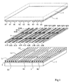
- the cathode assembly and lower grid of a screen according to the present invention is identical to classic realizations such as that described in the aforementioned US patent.
- This set is produced on an insulating substrate 1, for example a plate of glass.
- 2 microtips are formed on columns of cathode conductors K1, K2, K3 ... Rows of conductors grid L1, L2, L3 ... are formed on an insulating layer covering the cathode conductors.
- the ends of the microtips open out substantially at the level of the upper parts grid openings.
- this representation is very schematic and many variants known may be used, in particular, means for form a resistance between each microtip and the conductor associated cathode.
- the anode is similar to conventional anodes. Opposite of each cathode column K, three strips of luminescent material R, G, B also extending in columns. A difference from the state of the art is that these various bands, instead of being interconnected by bands of the same nature (the red bands, the green bands, the blue bands) are all brought to the same anode potential when screen operation.
- all the bands of phosphors can for example be formed on the same layer conductive 6 formed on a substrate 7.
- the layer 6 and the substrate 7 will be made of transparent materials, for example respectively a conductive oxide layer indium and tin (ITO) and a glass plate.
- the screen according to the present invention comprises a second grid with slots extending in the direction of columns whose width dimensions correspond substantially to those of the anode phosphor strips and respectively designated by the references A1R, A1G, A1B; A2R, A2G, A2B; A3R, A3G, A3B ...
- each slot corresponds to a strip of luminophore and we will speak below, for the sake of simplicity of "red slit”, “green slit”, “blue slit”.
- this second grid was formed of an insulating material and that the inner edges of each of the slots were coated lateral metallization M1R, M1G, M1B; M2R, M2G, M2B; M3R, M3G, M3B ...
- the lateral metallizations corresponding to slots associated with the same color are connected to the same terminal (not shown), that is to say that the metallizations M1R, M2R, M3R ... are connected to the same terminal as are the metallizations M1G, M2G, M3G ... and M1B, M2B, M3B ...
- isolation and spacing means are provided between the second grid and the upper face of the first grid, and between the second grid and the underside of the anode.
- the addressing mode of this device will be substantially the same as described in the aforementioned US patent except that, instead of switching the phosphor bands anode, metallization switching is carried out side of the slots of the second grid.
- the advantage of the present invention emerges from an analysis typical values of the potentials to be applied to the various screen electrodes.
- red pixels corresponding to row L2 of the first grid This row L2 will be placed at a potential of around 80 volts, the others rows L1, L3 ... being grounded. Columns K1, K2, K3 ... will be at potentials of the order of 0 to 30 volts depending on the brightness desired pixels considered.
- MR metallizations (M1R, M2R, M3R ) red slots in the second grid will be placed at a potential of +10 V relative to ground for let through the electrons emitted by the underlying spikes towards the red phosphors.
- the MG and MB metallizations of green and blue slots will be placed at a potential of -10 V relative to mass to block the electrons that would be normally directed through them towards the green phosphors and blue. It will be noted that this second grid has not only a shutter function but also a focusing function. We is therefore assured that when the "red slits" of the second grid are validated, only red phosphors will be bombed. This focusing effect will be optimized by an adjustment of the color selection potential applied to the slots in the second grid.
- Another advantage of the present invention is that, since there is no longer any need to switch the anode, this can be placed at a very high potential, for example several thousand of volts so the energy of the electrons will be much more high and will produce better illumination of the phosphors.
- these phosphors can then be coated on the side of their inner face with a thin conductive layer, for example a thin layer of aluminum which, in known manner, provides many advantages, in particular to avoid lighting phenomena parasites.
- an advantage additional of the present invention is that it allows use identical cathode and first grid systems to those already manufactured in the prior art and does not require so that a modification (a simplification) of the structure anode and making an additional grid.
- isolation and spacing systems may consist of spacing balls or perforated spacer plates.
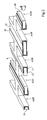
- FIG. 2 represents an exemplary embodiment according to the present invention of a second grid.
- This grid is made from a metal sheet 10 stamped to define the slots AR, AG, AB (only portions of the slots A2R, A2G, A2B, A3R, A3G are shown) and spacers stiffening 9.
- the AG slots are directly delimited by edges opposite the metal sheet 10.
- the slots AR and AB are defined by the facing edges of conductive layers 11 formed on an insulating layer 12 deposited on the metal sheet. The deposition and delimitation of these insulating layers and conductive may be carried out in a conventional manner. It is clear that all metallizations of AG slots are the same potential (that of the metallic foil). Likewise, metallizations of each of the AB slots and the metallizations of each AR slots will be brought to the same potential.
- one of the three electrodes of the second grid consists of the material of a metallic foil makes it particularly easy to interconnect the other two metallization groups of this grid which may by example be connected by metallic and insulated strips arranged at opposite ends of the metallizations of the slots.
- a such conductive plate can be very thin while having a good mechanical strength. Its thickness can for example be on the order of 1 to 5 tenths of a millimeter and the metal which constitutes, for example, aluminum, copper, stainless steel, nickel, an aluminum alloy.
- a grid according to the present invention may be used with a screen whose diagonal dimension is of the order of a meter, the dimensions of a pixel being of the order of a millimeter.
- the step of the grid will then be of the order of 0.15 mm, the distance between groups of three slots being of the order of 0.25 mm.
Landscapes
- Cathode-Ray Tubes And Fluorescent Screens For Display (AREA)
- Control Of Indicators Other Than Cathode Ray Tubes (AREA)
Claims (3)
- Mikrospitzen-Farb-Flachbildschirm, der folgendes umfaßt:gekennzeichnet durch:eine Kathode mit Mikrospitzen (2), welche in Spalten (K1, K2, K3...) aufgeteilt ist, die unabhängig adressierbar sind,ein erstes Gitter zur Auswahl von Bildpunkten, welches in Reihen (L1, L2, L3...) aufgeteilt ist, die unabhängig adressierbar sind,ein zweites Gitter zur Farbauswahl, das mehrere Gruppen von Schlitzen umfaßt, die sich entlang der Spaltenrichtung erstrecken, wobei jede Gruppe von drei Schlitzen (AiR, AiG, AiB) einer Kathodenspalte entspricht und Schlitze derselben Zeile jeder Gruppe mit einem gleichen Anschlußpunkt verbunden sind, undeine Anode, die Gruppen von drei parallelen Bändern in einer Spalte aus lumineszierendem Material dreier ausgewählter Farben (RGB) umfassen, wobei eine Gruppe von drei Bändern einer Kathodenspalte entspricht, jedes Band einem der Schlitze entspricht und alle Bänder aus lumineszierendem Material im Betrieb auf ein gleiches Potential gebracht werden.
- Bildschirm nach Anspruch 1, dadurch gekennzeichnet, daß das zweite Gitter durch Ausschneiden einer dünnen Metallfolie (10) gebildet ist, um darin die Schlitze und versteifende Abstandshalter (9) zu bilden, wobei eines von drei Bändern durch die zwei gegenüberliegenden Ränder der ausgeschnittenen Metallfolie festgelegt ist und die zwei anderen der drei Bänder durch die gegenüberliegenden Ränder leitender Schichten gebildet werden, welche auf einer isolierenden Schicht aufgebracht sind, die ihrerseits auf der Folie gebildet ist.
- Steuerverfahren für einen Bildschirm nach Anspruch 1, dadurch gekennzeichnet, daß es folgende Schritte umfaßt:die Anoden werden auf ein hohes Anodenpotential gebracht,die Schlitzmetallisierungen des zweiten Gitters, die einer ersten Farbe entsprechen, werden auf ein Freigabepotential gebracht, und die anderen Metallisierungen, die den zwei anderen Farben entsprechen, werden auf ein Sperrpotential gebracht,alle Zeilen des ersten Gitters werden sequentiell auf ein Adressierungspotential gebracht,nach dem Adressieren jeder Zeile des ersten Gitters werden die Kathodenspalten auf ein Potential vorgespannt, welches dafür ausgewählt ist, eine gewünschte Leuchtstärke der Bildpunkte der ausgewählten Farbe der Reihe zu erhalten,Wiederholen des Vorgangs für die zwei anderen Farben undWiederholen aller Vorgänge für die folgenden Einzelbilder.
Applications Claiming Priority (2)
| Application Number | Priority Date | Filing Date | Title |
|---|---|---|---|
| FR9605934A FR2748348B1 (fr) | 1996-05-06 | 1996-05-06 | Ecran couleur a micropointes a double grille |
| FR9605934 | 1996-05-06 |
Publications (2)
| Publication Number | Publication Date |
|---|---|
| EP0806790A1 EP0806790A1 (de) | 1997-11-12 |
| EP0806790B1 true EP0806790B1 (de) | 2003-02-19 |
Family
ID=9492082
Family Applications (1)
| Application Number | Title | Priority Date | Filing Date |
|---|---|---|---|
| EP97410051A Expired - Lifetime EP0806790B1 (de) | 1996-05-06 | 1997-05-02 | Mikrospitzen-Farbbildschirm mit zwei Gittern |
Country Status (5)
| Country | Link |
|---|---|
| US (1) | US6034658A (de) |
| EP (1) | EP0806790B1 (de) |
| JP (1) | JPH1055771A (de) |
| DE (1) | DE69719110T2 (de) |
| FR (1) | FR2748348B1 (de) |
Families Citing this family (2)
| Publication number | Priority date | Publication date | Assignee | Title |
|---|---|---|---|---|
| GB2321335A (en) * | 1997-01-16 | 1998-07-22 | Ibm | Display device |
| KR100463190B1 (ko) | 2002-06-12 | 2004-12-23 | 삼성에스디아이 주식회사 | 금속 메쉬 일체형 스페이서 구조체 및 이 구조체를 갖는평판 표시 소자 |
Family Cites Families (12)
| Publication number | Priority date | Publication date | Assignee | Title |
|---|---|---|---|---|
| JPS63150837A (ja) * | 1986-12-16 | 1988-06-23 | Canon Inc | 電子放出装置 |
| US5160871A (en) * | 1989-06-19 | 1992-11-03 | Matsushita Electric Industrial Co., Ltd. | Flat configuration image display apparatus and manufacturing method thereof |
| DE69026353T2 (de) * | 1989-12-19 | 1996-11-14 | Matsushita Electric Ind Co Ltd | Feldemissionsvorrichtung und Verfahren zur Herstellung derselben |
| US5150067A (en) * | 1990-04-16 | 1992-09-22 | Mcmillan Michael R | Electromagnetic pulse generator using an electron beam produced with an electron multiplier |
| US5424605A (en) * | 1992-04-10 | 1995-06-13 | Silicon Video Corporation | Self supporting flat video display |
| JPH06139918A (ja) * | 1992-10-23 | 1994-05-20 | Shimadzu Corp | 電子放出素子 |
| US5604394A (en) * | 1992-11-06 | 1997-02-18 | Mitsubishi Denki Kabushiki Kaisha | Image display apparatus |
| GB2285168B (en) * | 1993-12-22 | 1997-07-16 | Marconi Gec Ltd | Electron field emission devices |
| US5528103A (en) * | 1994-01-31 | 1996-06-18 | Silicon Video Corporation | Field emitter with focusing ridges situated to sides of gate |
| US5650690A (en) * | 1994-11-21 | 1997-07-22 | Candescent Technologies, Inc. | Backplate of field emission device with self aligned focus structure and spacer wall locators |
| FR2732159B1 (fr) * | 1995-03-22 | 1997-06-13 | Pixtech Sa | Ecran plat de visualisation a double grille |
| US5760858A (en) * | 1995-04-21 | 1998-06-02 | Texas Instruments Incorporated | Field emission device panel backlight for liquid crystal displays |
-
1996
- 1996-05-06 FR FR9605934A patent/FR2748348B1/fr not_active Expired - Fee Related
-
1997
- 1997-05-02 DE DE69719110T patent/DE69719110T2/de not_active Expired - Fee Related
- 1997-05-02 EP EP97410051A patent/EP0806790B1/de not_active Expired - Lifetime
- 1997-05-06 US US08/851,732 patent/US6034658A/en not_active Expired - Fee Related
- 1997-05-06 JP JP9130555A patent/JPH1055771A/ja not_active Withdrawn
Also Published As
| Publication number | Publication date |
|---|---|
| US6034658A (en) | 2000-03-07 |
| DE69719110T2 (de) | 2003-10-09 |
| JPH1055771A (ja) | 1998-02-24 |
| FR2748348A1 (fr) | 1997-11-07 |
| DE69719110D1 (de) | 2003-03-27 |
| EP0806790A1 (de) | 1997-11-12 |
| FR2748348B1 (fr) | 1998-07-24 |
Similar Documents
| Publication | Publication Date | Title |
|---|---|---|
| EP0704877B1 (de) | Elektrischer Schutz von einer Anode eines flachen Bildschirms | |
| FR2708380A1 (fr) | Dispositif d'affichage d'images et circuit de commande associé. | |
| FR2753002A1 (fr) | Dispositif d'affichage a emission de champ | |
| FR2682211A1 (fr) | Dispositif d'affichage fluorescent de type plat. | |
| EP0867912A1 (de) | Montieren von Abstandshältern in einer flachen Anzeigetafel | |
| EP0806790B1 (de) | Mikrospitzen-Farbbildschirm mit zwei Gittern | |
| EP1139374A1 (de) | Kathodenplatte für einen flachen Bildschirm | |
| FR2626732A1 (fr) | Dispositif de visualisation en couleurs-monochrome | |
| EP0734042B1 (de) | Anode eines flachen Bildschirms mit Widerstandsstreifen | |
| FR2714209A1 (fr) | Dispositif d'affichage. | |
| EP0734043B1 (de) | Doppel-Gate-Flaches Bildschirm | |
| EP0817232B1 (de) | Verfahren zur Regenerierung von Mikrospitzen einer flachen Anzeigetafel | |
| FR2731291A1 (fr) | Circuit de commande pour un dispositif d'affichage d'image | |
| EP0649162B1 (de) | Flaches Kaltkathodeanzeigegerät mit geschalteter Anode | |
| EP1032017B1 (de) | Anode mit Widerstand für einen flachen Bildschirm | |
| EP0877407A1 (de) | Anode eines flachen Bildschirms | |
| EP0844643A1 (de) | Flaches Bildschirm mit seitlicher Ablenkung | |
| EP0844642A1 (de) | Flaches Bildschirm mit fokussierenden Gittern | |
| EP0732723B1 (de) | Flaches Bildschirm mit hohem Inter-Elektrodenabstand | |
| EP0806787B1 (de) | Herstellung einer Anode eines flachen Bildschirms | |
| FR2770338A1 (fr) | Elimination de l'effet de moire d'un ecran plat de visualisation | |
| EP1073088A1 (de) | Herstellung einer Anode eines flachen Bildschirms, nach diesem Verfahren hergestellte Anode und Verwendung dieser Anode für einen flachen Schirm | |
| FR2761522A1 (fr) | Uniformisation de l'emission electronique potentielle d'une cathode d'ecran plat a micropointes | |
| WO2000075952A1 (fr) | Panneaux a plasma de type matriciel | |
| EP1956625B1 (de) | Struktur zum Aussenden von Elektronen durch Feldeffekt mit Fokussierung der Aussendung |
Legal Events
| Date | Code | Title | Description |
|---|---|---|---|
| PUAI | Public reference made under article 153(3) epc to a published international application that has entered the european phase |
Free format text: ORIGINAL CODE: 0009012 |
|
| AK | Designated contracting states |
Kind code of ref document: A1 Designated state(s): DE FR GB IT |
|
| 17P | Request for examination filed |
Effective date: 19980421 |
|
| 17Q | First examination report despatched |
Effective date: 20000118 |
|
| 111Z | Information provided on other rights and legal means of execution |
Free format text: 20000403 DE FR GB IT |
|
| GRAG | Despatch of communication of intention to grant |
Free format text: ORIGINAL CODE: EPIDOS AGRA |
|
| GRAG | Despatch of communication of intention to grant |
Free format text: ORIGINAL CODE: EPIDOS AGRA |
|
| GRAG | Despatch of communication of intention to grant |
Free format text: ORIGINAL CODE: EPIDOS AGRA |
|
| GRAH | Despatch of communication of intention to grant a patent |
Free format text: ORIGINAL CODE: EPIDOS IGRA |
|
| GRAH | Despatch of communication of intention to grant a patent |
Free format text: ORIGINAL CODE: EPIDOS IGRA |
|
| GRAA | (expected) grant |
Free format text: ORIGINAL CODE: 0009210 |
|
| AK | Designated contracting states |
Designated state(s): DE FR GB IT |
|
| REG | Reference to a national code |
Ref country code: GB Ref legal event code: FG4D Free format text: NOT ENGLISH |
|
| REF | Corresponds to: |
Ref document number: 69719110 Country of ref document: DE Date of ref document: 20030327 Kind code of ref document: P |
|
| 29U | Proceedings interrupted after grant according to rule 142 epc |
Effective date: 20020621 |
|
| PG25 | Lapsed in a contracting state [announced via postgrant information from national office to epo] |
Ref country code: GB Free format text: LAPSE BECAUSE OF NON-PAYMENT OF DUE FEES Effective date: 20030519 |
|
| GBT | Gb: translation of ep patent filed (gb section 77(6)(a)/1977) | ||
| PG25 | Lapsed in a contracting state [announced via postgrant information from national office to epo] |
Ref country code: DE Free format text: LAPSE BECAUSE OF NON-PAYMENT OF DUE FEES Effective date: 20031202 |
|
| GBPC | Gb: european patent ceased through non-payment of renewal fee |
Effective date: 20030519 |
|
| PG25 | Lapsed in a contracting state [announced via postgrant information from national office to epo] |
Ref country code: FR Free format text: LAPSE BECAUSE OF NON-PAYMENT OF DUE FEES Effective date: 20040130 |
|
| REG | Reference to a national code |
Ref country code: FR Ref legal event code: ST |
|
| PG25 | Lapsed in a contracting state [announced via postgrant information from national office to epo] |
Ref country code: IT Free format text: LAPSE BECAUSE OF NON-PAYMENT OF DUE FEES Effective date: 20050502 |
|
| RIC2 | Information provided on ipc code assigned after grant |
Ipc: H01J 31/12 20060101AFI19970628BHEP |
|
| 29W | Proceedings resumed after grant [after interruption of proceedings according to rule 142 epc] |
Effective date: 20210201 |
|
| PUAJ | Public notification under rule 129 epc |
Free format text: ORIGINAL CODE: 0009425 |
|
| 32PN | Public notification |
Free format text: NOTIFICATION ETABLIE CONFORMEMENT A LA REGLE 142 CBE (REPRISE DE LA PROCEDURE CONFORMEMENT A LA REGLE 142 (2) CBE EN DATE DU 17.08.2020) |
|
| PLBE | No opposition filed within time limit |
Free format text: ORIGINAL CODE: 0009261 |
|
| STAA | Information on the status of an ep patent application or granted ep patent |
Free format text: STATUS: NO OPPOSITION FILED WITHIN TIME LIMIT |
|
| 26N | No opposition filed |
Effective date: 20211103 |