EP0806684A1 - Module d'émission et de réception optique - Google Patents
Module d'émission et de réception optique Download PDFInfo
- Publication number
- EP0806684A1 EP0806684A1 EP96107309A EP96107309A EP0806684A1 EP 0806684 A1 EP0806684 A1 EP 0806684A1 EP 96107309 A EP96107309 A EP 96107309A EP 96107309 A EP96107309 A EP 96107309A EP 0806684 A1 EP0806684 A1 EP 0806684A1
- Authority
- EP
- European Patent Office
- Prior art keywords
- laser
- light
- laser diode
- wavelength
- module according
- Prior art date
- Legal status (The legal status is an assumption and is not a legal conclusion. Google has not performed a legal analysis and makes no representation as to the accuracy of the status listed.)
- Withdrawn
Links
Images


Classifications
-
- H—ELECTRICITY
- H01—ELECTRIC ELEMENTS
- H01S—DEVICES USING THE PROCESS OF LIGHT AMPLIFICATION BY STIMULATED EMISSION OF RADIATION [LASER] TO AMPLIFY OR GENERATE LIGHT; DEVICES USING STIMULATED EMISSION OF ELECTROMAGNETIC RADIATION IN WAVE RANGES OTHER THAN OPTICAL
- H01S5/00—Semiconductor lasers
- H01S5/10—Construction or shape of the optical resonator, e.g. extended or external cavity, coupled cavities, bent-guide, varying width, thickness or composition of the active region
- H01S5/1082—Construction or shape of the optical resonator, e.g. extended or external cavity, coupled cavities, bent-guide, varying width, thickness or composition of the active region with a special facet structure, e.g. structured, non planar, oblique
-
- G—PHYSICS
- G02—OPTICS
- G02B—OPTICAL ELEMENTS, SYSTEMS OR APPARATUS
- G02B6/00—Light guides; Structural details of arrangements comprising light guides and other optical elements, e.g. couplings
- G02B6/24—Coupling light guides
- G02B6/42—Coupling light guides with opto-electronic elements
- G02B6/4201—Packages, e.g. shape, construction, internal or external details
- G02B6/4246—Bidirectionally operating package structures
-
- H—ELECTRICITY
- H01—ELECTRIC ELEMENTS
- H01S—DEVICES USING THE PROCESS OF LIGHT AMPLIFICATION BY STIMULATED EMISSION OF RADIATION [LASER] TO AMPLIFY OR GENERATE LIGHT; DEVICES USING STIMULATED EMISSION OF ELECTROMAGNETIC RADIATION IN WAVE RANGES OTHER THAN OPTICAL
- H01S5/00—Semiconductor lasers
- H01S5/02—Structural details or components not essential to laser action
- H01S5/022—Mountings; Housings
- H01S5/023—Mount members, e.g. sub-mount members
- H01S5/02325—Mechanically integrated components on mount members or optical micro-benches
- H01S5/02326—Arrangements for relative positioning of laser diodes and optical components, e.g. grooves in the mount to fix optical fibres or lenses
-
- G—PHYSICS
- G02—OPTICS
- G02B—OPTICAL ELEMENTS, SYSTEMS OR APPARATUS
- G02B6/00—Light guides; Structural details of arrangements comprising light guides and other optical elements, e.g. couplings
- G02B6/24—Coupling light guides
- G02B6/42—Coupling light guides with opto-electronic elements
- G02B6/4201—Packages, e.g. shape, construction, internal or external details
- G02B6/4219—Mechanical fixtures for holding or positioning the elements relative to each other in the couplings; Alignment methods for the elements, e.g. measuring or observing methods especially used therefor
- G02B6/4228—Passive alignment, i.e. without a detection of the degree of coupling or the position of the elements
- G02B6/423—Passive alignment, i.e. without a detection of the degree of coupling or the position of the elements using guiding surfaces for the alignment
-
- H—ELECTRICITY
- H01—ELECTRIC ELEMENTS
- H01S—DEVICES USING THE PROCESS OF LIGHT AMPLIFICATION BY STIMULATED EMISSION OF RADIATION [LASER] TO AMPLIFY OR GENERATE LIGHT; DEVICES USING STIMULATED EMISSION OF ELECTROMAGNETIC RADIATION IN WAVE RANGES OTHER THAN OPTICAL
- H01S5/00—Semiconductor lasers
- H01S5/02—Structural details or components not essential to laser action
- H01S5/022—Mountings; Housings
- H01S5/0225—Out-coupling of light
- H01S5/02251—Out-coupling of light using optical fibres
-
- H—ELECTRICITY
- H01—ELECTRIC ELEMENTS
- H01S—DEVICES USING THE PROCESS OF LIGHT AMPLIFICATION BY STIMULATED EMISSION OF RADIATION [LASER] TO AMPLIFY OR GENERATE LIGHT; DEVICES USING STIMULATED EMISSION OF ELECTROMAGNETIC RADIATION IN WAVE RANGES OTHER THAN OPTICAL
- H01S5/00—Semiconductor lasers
- H01S5/02—Structural details or components not essential to laser action
- H01S5/022—Mountings; Housings
- H01S5/0225—Out-coupling of light
- H01S5/02255—Out-coupling of light using beam deflecting elements
Definitions
- the invention relates to an optical transmission and reception module for bidirectional transmission with wavelength division multiplexing with a laser diode for transmitting light of a first wavelength, with a reception diode for receiving light of a second wavelength and with an optical waveguide end for transmitting light of the two predetermined wavelengths.
- a micro-optical multiplexer is known from DE 38 01 764. Using anisotropic etching technology, V-grooves and recesses are made on a silicon substrate, into which ball lenses, glass fibers and filter plates can be inserted.
- An optical transmission and reception module for bidirectional transmission with wavelength division multiplexing in an arrangement designed according to this prior art consists of a laser diode, a filter plate, a reception diode and an optical fiber end, which are inserted into corresponding recesses in the silicon carrier. Lenses are provided between the individual components and the filter plate for beam adaptation. The manufacture of the holders for the filter plate is very complex.
- a laser diode with a wavelength-selective coating in an optical transmitter and receiver module for bidirectional transmission with wavelength division multiplex results in the advantage that there is no need to use individual filter plates and that they therefore do not have to be fixed and adjusted in holders.
- the coating provided on the laser diode can already be carried out during the manufacture of the laser diode using the known methods of semiconductor technology.
- a coating of the light-emitting laser end surface is required anyway in order to passivate the laser end surface.
- it is necessary that the direction of the wave guide in the laser and the light-emitting laser end face are at an angle other than 90 °. Therefore, a laser must be used whose function as a laser is not based on the reflection at the crystal end faces. This criterion is met, for example, by DFB or DBR lasers. With these lasers, it is even advantageous if the light at the crystal end faces is not reflected back into the waveguide.
- At least one light-emitting end surface is arranged at a certain angle to the end of the optical waveguide and to the receiving diode and to the direction of the wave guide in the laser.
- the second laser end surface can be selected in such a way that it is the most economical in terms of production technology, for example for the utilization of crystal planes. It is particularly advantageous to choose the side surfaces in such a way that they can be arranged in a silicon carrier parallel to the side surfaces of anisotropically etched guide grooves. This saves additional adjustment steps when mounting the laser diode on a silicon carrier.
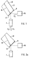
- FIG. 1 shows an optical transmitter and receiver module according to the invention for bidirectional transmission with wavelength division multiplexing.
- a laser diode LD is provided for transmitting light of a first wavelength ⁇ 1 .
- a reception diode PD is also provided for receiving light of a second wavelength ⁇ 2 .
- an optical fiber end F is provided, which serves to transmit light of the two predetermined wavelengths ⁇ 1 and ⁇ 2 .
- the laser diode LD is, for example, a DFB or a DBR laser, the function of which is not based on the reflection of the Light based on the laser end faces.
- the position of the waveguide W in the laser diode LD is indicated by a dash.
- the direction of the waveguide in the laser diode LD is therefore parallel to the position of the waveguide W.
- the laser side surfaces LS run parallel to the waveguide W.
- a light-emitting laser end surface LE is not perpendicular to the direction of the waveguide W and thus to the direction of the waveguide in the laser diode LD.
- the end surface LE and the direction of the wave guide are at an angle other than 90 °.
- This laser end surface LE, which is inclined to the direction of the wave guide has a wavelength-selective coating B.
- the coating B is transparent to light of the wavelength ⁇ 1 and reflective to light of the wavelength ⁇ 2 .
- Light from the fiber end F of the wavelength ⁇ 2 is reflected on the coating B and falls on the receiving diode PD.
- Light from the laser diode LD with the wavelength ⁇ 1 is transmitted through the wavelength-selective coating B, is refracted when it emerges from the coating and is then coupled into the end of the optical waveguide.
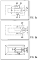
- the waveguide W is arranged inclined to the side faces in a rectangular laser diode (FIG. 2a). It is also possible that the laser diode is diamond-shaped in section and the waveguide is arranged parallel to the side surfaces of the laser diode (FIG. 2b).
- the angle ⁇ between incident light and reflected light can also be chosen to be not equal to 90 °. It is not necessary that both light-emitting laser end faces are inclined toward the waveguide W.
- the light-emitting end surface which is not used, can be any angle ⁇ to the perpendicular on the side surface of the laser diodes LD exhibit.
- the side surface of the laser diode and the fiber axis can be arranged parallel to one another (FIG. 2c).
- FIG. 2d shows an arrangement in which the angle between the beam path from the fiber F to the laser diode LD and from the laser diode LD to the receiving diode PD is 90 °. Since the position of the waveguide in the laser diode and the angle of the laser end face LE can be freely selected, the angle ⁇ can be determined as desired.
- FIG. 3 shows an arrangement according to FIG. 2d, which is introduced into a silicon carrier T with anisotropically etched V-grooves and depressions.
- a ball lens K1, K2 is provided between the receiving diode PD and the optical waveguide F and the laser diode LD, with which a beam adaptation and focusing is carried out.
- the receiving diode PD is not mounted in a recess, but on the silicon carrier T.
- a section from A to B is shown, which shows that the light beam falling on the photodiode is reflected on the inclined end face of the V-groove and falls on the photodiode.
- One side surface of the laser diode is arranged parallel to the optical waveguide F. Due to the anisotropic etching technique, stops in the silicon carrier T are etched, which are parallel to this side surface and which simplify the adjustment of the laser diode. This means that the position of the laser diode is only fixed in one direction.
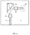
- FIG. 4 shows a corresponding arrangement in which the second light-emitting laser end face is at a right angle to the side face of the laser. Since stops on the silicon carrier T also have a right angle to one another when they have been anisotropically etched, it is thereby possible to adjust the laser diode LD in both directions with the aid of these stops.
- a problem with the exemplary embodiments described so far is that a beam transformation is required between the laser diode and the fiber because of the different beam characteristics of the laser diode and the single-mode fiber.
- the beam guided in the fiber must be transformed so that it has approximately the same divergence as the laser on the end face of the laser.
- the received beam reflected on the laser face will therefore have a very large divergence.
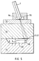
- For an effective coupling of a photodiode it must either have a very large active area, which has a disadvantageous effect on the achievable cutoff frequency, or the photodiode must sit very close to the laser end face, which results in space problems and problems with electrical crosstalk, or it must also have a coupling optics be used. This problem does not occur in the following exemplary embodiment (FIG. 5).
- the laser diode LD is seated on a recess anisotropically etched in a silicon carrier T1 with a flat bottom and side surfaces SF inclined by 54.7 °, at least one of which is mirrored.
- the light-emitting end surface of the laser ends as close as possible in front of a mirrored side surface of the depression.
- the received light beam emerging from the fiber strikes the laser end face after passing through the lens L1 and after reflection on the side face SF and is reflected there at the angle - ⁇ . After a further reflection on the side face SF, it passes through the lens L2 and is focused into the receiving photodiode PD.
- the angle ⁇ must be at least as large as the horizontal far field angle of the laser in order to separate the transmit and To reach the receiving beam.
- Another carrier T2 with two lenses is attached in a plane parallel to the surface of the silicon carrier above the silicon carrier with the recess V for receiving the laser (FIG. 6b).
- These lenses can be, for example, microstructured Fresnel lenses on a support made of glass or silicon or another suitable material. Holographically produced lenses are also possible. Lenses that can be produced in silicon by known dry etching processes are also suitable here.
- the lenses are symmetrical about a plane of symmetry E s , which contains the surface normal of the laser end face, the light exit window of the laser and the surface normal of the silicon carrier.
- This plane is the yz plane of a right-angled coordinate system, the z axis of which is the surface normal of the laser end face and the y axis of which is the surface normal of the silicon substrate.
- the x-axis lies in the active layer of the laser.
- One lens lies in the beam path of the laser or the received signal emerging from the fiber and the other lies in the beam path of the reflected signal on the laser end face Received signal.
- the light exit window of the laser is imaged on the two image points B1 and B2, which have a distance b in the beam direction from the respective lenses (FIG. 6c).
- the fiber and the photodiode are mounted above the lens plane.
- the image point for the fiber is, due to the two imaging with M and 1 / M, just as large as the mode field diameter of the fiber, which is 10 ⁇ m with standard single mode fibers.
- Mounting tolerances of the laser relative to the lens carrier plate have a similar effect on the position of the two pixels B 1 and B 2 and are enlarged in accordance with the magnification ratio M of the figure.
- the misalignment of the laser has no effect on the mutual distance d b of the two pixels. This distance is determined by the distance between the lens centers d 1 and to a small extent by the object and image width.
- the adjustment of the fiber which is necessary to compensate for the assembly tolerances of the laser, also simultaneously adjusts the photodiode with almost the same accuracy. Because of this and because of the small size of the beam waist in the pixel B 2 , a photodiode with a very small diameter can be used the active zone, which allows very high cut-off frequencies in the GHz range. With a diameter of the active zone of the photodiode of 30 ⁇ m, there are still lateral tolerances to the position of the fiber core of ⁇ 10 ⁇ m for the mounting of the photodiode on the common carrier, which can still be achieved with passive mounting with the aid of alignment marks.
- the fiber Since the beam path is inclined relative to the normal to the substrate surface by the directional angles ⁇ zy and ⁇ xy , either the fiber must also be inclined in this way, or this inclination must be compensated for by mounting the fiber vertically by means of a corresponding grinding angle of the fiber end face. The latter would have the advantage of avoiding harmful back reflections from the face of the fiber onto the laser. Horizontal mounting of the fiber, for example in an anisotropically etched silicon carrier with a V-groove for receiving the fiber, is also possible. The received and transmitted light bundle is then deflected on the mirrored end face of the fiber V-groove (see FIG. 7).
- a second proposal for beam guidance is shown in FIG. 8.
- the laser chip is also mounted on the bottom of a recess.
- the laser does not sit here with its edge parallel to the foot edge of one side surface of the recess, but in front of a corner of two adjacent mirrored side surfaces, so that the transmitted light beam hits one side surface and the reception light beam hits the other side surface.
- the two light beams of the transmission and reception beam reflected on the side surfaces intersect.
- a single lens for both beams is placed in the crossing point. Since both beams emanate from different mirror images of the laser, corresponding to the reflection on the different side surfaces also their pixels despite the image with only one lens at different locations B 1 and B 2 .
- the assembly and adjustment of fiber and photodiode is carried out in these pixels, as stated in proposal 1.
Landscapes
- Physics & Mathematics (AREA)
- General Physics & Mathematics (AREA)
- Optics & Photonics (AREA)
- Condensed Matter Physics & Semiconductors (AREA)
- Electromagnetism (AREA)
- Optical Couplings Of Light Guides (AREA)
Priority Applications (1)
| Application Number | Priority Date | Filing Date | Title |
|---|---|---|---|
| EP96107309A EP0806684A1 (fr) | 1996-05-09 | 1996-05-09 | Module d'émission et de réception optique |
Applications Claiming Priority (1)
| Application Number | Priority Date | Filing Date | Title |
|---|---|---|---|
| EP96107309A EP0806684A1 (fr) | 1996-05-09 | 1996-05-09 | Module d'émission et de réception optique |
Publications (1)
| Publication Number | Publication Date |
|---|---|
| EP0806684A1 true EP0806684A1 (fr) | 1997-11-12 |
Family
ID=8222765
Family Applications (1)
| Application Number | Title | Priority Date | Filing Date |
|---|---|---|---|
| EP96107309A Withdrawn EP0806684A1 (fr) | 1996-05-09 | 1996-05-09 | Module d'émission et de réception optique |
Country Status (1)
| Country | Link |
|---|---|
| EP (1) | EP0806684A1 (fr) |
Citations (5)
| Publication number | Priority date | Publication date | Assignee | Title |
|---|---|---|---|---|
| DE3801764A1 (de) * | 1988-01-22 | 1989-08-03 | Ant Nachrichtentech | Wellenlaengenmultiplexer oder -demultiplexer, sowie verfahren zur herstellung des wellenlaengenmultiplexers oder -demultiplexers |
| JPH01238082A (ja) * | 1988-03-18 | 1989-09-22 | Nippon Telegr & Teleph Corp <Ntt> | 半導体レーザ |
| DE9319378U1 (de) * | 1993-12-16 | 1994-02-17 | Siemens AG, 80333 München | Kombinierte Sende- und Empfangsstation für die optische Nachrichtenübertragung |
| EP0631163A1 (fr) * | 1993-05-17 | 1994-12-28 | Siemens Aktiengesellschaft | Emetteur-récepteur optique bidirectionnel |
| DE4407451C1 (de) * | 1994-03-05 | 1995-05-04 | Ant Nachrichtentech | Wellenlängenduplexer |
-
1996
- 1996-05-09 EP EP96107309A patent/EP0806684A1/fr not_active Withdrawn
Patent Citations (5)
| Publication number | Priority date | Publication date | Assignee | Title |
|---|---|---|---|---|
| DE3801764A1 (de) * | 1988-01-22 | 1989-08-03 | Ant Nachrichtentech | Wellenlaengenmultiplexer oder -demultiplexer, sowie verfahren zur herstellung des wellenlaengenmultiplexers oder -demultiplexers |
| JPH01238082A (ja) * | 1988-03-18 | 1989-09-22 | Nippon Telegr & Teleph Corp <Ntt> | 半導体レーザ |
| EP0631163A1 (fr) * | 1993-05-17 | 1994-12-28 | Siemens Aktiengesellschaft | Emetteur-récepteur optique bidirectionnel |
| DE9319378U1 (de) * | 1993-12-16 | 1994-02-17 | Siemens AG, 80333 München | Kombinierte Sende- und Empfangsstation für die optische Nachrichtenübertragung |
| DE4407451C1 (de) * | 1994-03-05 | 1995-05-04 | Ant Nachrichtentech | Wellenlängenduplexer |
Non-Patent Citations (3)
| Title |
|---|
| BUUS J ET AL: "REFLECTIVITY OF COATED AND TILTED SEMICONDUCTOR FACETS", IEEE JOURNAL OF QUANTUM ELECTRONICS, vol. 27, no. 6, 1 June 1991 (1991-06-01), pages 1837 - 1842, XP000230003 * |
| LIN C F: "SUPERLUMINESCENT DIODES WITH ANGLED FACET ETCHED BY CHEMICALLY ASSISTED ION BEAM ETCHING", ELECTRONICS LETTERS, vol. 27, no. 11, 23 May 1991 (1991-05-23), pages 968 - 970, XP000232452 * |
| PATENT ABSTRACTS OF JAPAN vol. 013, no. 568 (E - 861) 15 December 1989 (1989-12-15) * |
Similar Documents
| Publication | Publication Date | Title |
|---|---|---|
| DE19610881B4 (de) | Mikrosystembaustein | |
| EP0395854B1 (fr) | Arrangement pour coupler un guide d'onde avec un émetteur ou récepteur optique | |
| DE102005019562B4 (de) | Optisches Sende- und Empfangsmodul | |
| DE4440976A1 (de) | Optische Sende- und Empfangseinrichtung mit einem oberflächenemittierenden Laser | |
| EP0238977B1 (fr) | Module émission-réception pour un réseau de communication bidirectionnelle, particulièrement un RNIS à large bande | |
| DE3687063T2 (de) | Optische komponente mit wellenleiter. | |
| DE10105943B4 (de) | Faseroptisches Linsensystem zum Koppeln von Fasern mit oberflächenbefestigten Bauelementen | |
| EP0713113A1 (fr) | Dispositif optique émetteur et récepteur | |
| DE60214186T2 (de) | Verfahren zur Herstellung von optischen Faserkollimatoren im Array | |
| DE10238741A1 (de) | Planare optische Komponente und Kopplungsvorrichtung zur Kopplung von Licht zwischen einer planaren optischen Komponente und einem optischen Bauteil | |
| EP0664585A1 (fr) | Module de transmission et de réception pour système de communication bidirectionnel | |
| EP0735397A2 (fr) | Dispositif micro-optique pour transformer des faisceaux d'un arrangement de diodes laser et procédé de fabrication d'un tel dispositif | |
| EP0660467A1 (fr) | Elément optoélectronique et sa méthode de fabrication | |
| DE10043985A1 (de) | Optischer Modifizierer und Verfahren zur Herstellung hierfür | |
| DE69806300T2 (de) | Untereinheit und Verfahren zur Kopplung optischer Elemente | |
| EP0815479B1 (fr) | Emetteur-recepteur optique | |
| DE69015588T2 (de) | Optischer Kopf integrierbar in einem hybriden Schaltkreis. | |
| DE69727343T2 (de) | Optoelektronisches Modul | |
| DE4301456C1 (de) | Anordnung zur Ankopplung eines Lichtwellenleiters | |
| DE19607107A1 (de) | Anordnung zur Kopplung von Signallicht zwischen einem Lichtwellenleiter und einer optoelektronischen Komponente | |
| DE19515688C1 (de) | Optisches Sende- und Empfangsmodul | |
| DE4313493A1 (de) | Anordnung zur Ankopplung eines Lichtwellenleiters an ein lichtaussendendes oder -empfangendes Element | |
| DE102005010557B4 (de) | Optischer Multiplexer/Demultiplexer | |
| DE102004038530B3 (de) | Verfahren und Vorrichtung zur Herstellung einer optischen Verbindung zwischen einem optoelektronischen Bauelement und einem Lichtwellenleiter | |
| DE19810624A1 (de) | Elektrooptisches Modul |
Legal Events
| Date | Code | Title | Description |
|---|---|---|---|
| PUAI | Public reference made under article 153(3) epc to a published international application that has entered the european phase |
Free format text: ORIGINAL CODE: 0009012 |
|
| AK | Designated contracting states |
Kind code of ref document: A1 Designated state(s): CH DE ES FR GB IT LI SE |
|
| 17P | Request for examination filed |
Effective date: 19980512 |
|
| RAP1 | Party data changed (applicant data changed or rights of an application transferred) |
Owner name: MARCONI COMMUNICATIONS GMBH |
|
| RAP1 | Party data changed (applicant data changed or rights of an application transferred) |
Owner name: MARCONI UK INTELLECTUAL PROPERTY LTD |
|
| GRAP | Despatch of communication of intention to grant a patent |
Free format text: ORIGINAL CODE: EPIDOSNIGR1 |
|
| STAA | Information on the status of an ep patent application or granted ep patent |
Free format text: STATUS: THE APPLICATION IS DEEMED TO BE WITHDRAWN |
|
| 18D | Application deemed to be withdrawn |
Effective date: 20040309 |