EP0806684A1 - Optical transmitting and receiving module - Google Patents
Optical transmitting and receiving module Download PDFInfo
- Publication number
- EP0806684A1 EP0806684A1 EP96107309A EP96107309A EP0806684A1 EP 0806684 A1 EP0806684 A1 EP 0806684A1 EP 96107309 A EP96107309 A EP 96107309A EP 96107309 A EP96107309 A EP 96107309A EP 0806684 A1 EP0806684 A1 EP 0806684A1
- Authority
- EP
- European Patent Office
- Prior art keywords
- laser
- light
- laser diode
- wavelength
- module according
- Prior art date
- Legal status (The legal status is an assumption and is not a legal conclusion. Google has not performed a legal analysis and makes no representation as to the accuracy of the status listed.)
- Withdrawn
Links
Images



Classifications
-
- H—ELECTRICITY
- H01—ELECTRIC ELEMENTS
- H01S—DEVICES USING THE PROCESS OF LIGHT AMPLIFICATION BY STIMULATED EMISSION OF RADIATION [LASER] TO AMPLIFY OR GENERATE LIGHT; DEVICES USING STIMULATED EMISSION OF ELECTROMAGNETIC RADIATION IN WAVE RANGES OTHER THAN OPTICAL
- H01S5/00—Semiconductor lasers
- H01S5/10—Construction or shape of the optical resonator, e.g. extended or external cavity, coupled cavities, bent-guide, varying width, thickness or composition of the active region
- H01S5/1082—Construction or shape of the optical resonator, e.g. extended or external cavity, coupled cavities, bent-guide, varying width, thickness or composition of the active region with a special facet structure, e.g. structured, non planar, oblique
-
- G—PHYSICS
- G02—OPTICS
- G02B—OPTICAL ELEMENTS, SYSTEMS OR APPARATUS
- G02B6/00—Light guides; Structural details of arrangements comprising light guides and other optical elements, e.g. couplings
- G02B6/24—Coupling light guides
- G02B6/42—Coupling light guides with opto-electronic elements
- G02B6/4201—Packages, e.g. shape, construction, internal or external details
- G02B6/4246—Bidirectionally operating package structures
-
- H—ELECTRICITY
- H01—ELECTRIC ELEMENTS
- H01S—DEVICES USING THE PROCESS OF LIGHT AMPLIFICATION BY STIMULATED EMISSION OF RADIATION [LASER] TO AMPLIFY OR GENERATE LIGHT; DEVICES USING STIMULATED EMISSION OF ELECTROMAGNETIC RADIATION IN WAVE RANGES OTHER THAN OPTICAL
- H01S5/00—Semiconductor lasers
- H01S5/02—Structural details or components not essential to laser action
- H01S5/022—Mountings; Housings
- H01S5/023—Mount members, e.g. sub-mount members
- H01S5/02325—Mechanically integrated components on mount members or optical micro-benches
- H01S5/02326—Arrangements for relative positioning of laser diodes and optical components, e.g. grooves in the mount to fix optical fibres or lenses
-
- G—PHYSICS
- G02—OPTICS
- G02B—OPTICAL ELEMENTS, SYSTEMS OR APPARATUS
- G02B6/00—Light guides; Structural details of arrangements comprising light guides and other optical elements, e.g. couplings
- G02B6/24—Coupling light guides
- G02B6/42—Coupling light guides with opto-electronic elements
- G02B6/4201—Packages, e.g. shape, construction, internal or external details
- G02B6/4219—Mechanical fixtures for holding or positioning the elements relative to each other in the couplings; Alignment methods for the elements, e.g. measuring or observing methods especially used therefor
- G02B6/4228—Passive alignment, i.e. without a detection of the degree of coupling or the position of the elements
- G02B6/423—Passive alignment, i.e. without a detection of the degree of coupling or the position of the elements using guiding surfaces for the alignment
-
- H—ELECTRICITY
- H01—ELECTRIC ELEMENTS
- H01S—DEVICES USING THE PROCESS OF LIGHT AMPLIFICATION BY STIMULATED EMISSION OF RADIATION [LASER] TO AMPLIFY OR GENERATE LIGHT; DEVICES USING STIMULATED EMISSION OF ELECTROMAGNETIC RADIATION IN WAVE RANGES OTHER THAN OPTICAL
- H01S5/00—Semiconductor lasers
- H01S5/02—Structural details or components not essential to laser action
- H01S5/022—Mountings; Housings
- H01S5/0225—Out-coupling of light
- H01S5/02251—Out-coupling of light using optical fibres
-
- H—ELECTRICITY
- H01—ELECTRIC ELEMENTS
- H01S—DEVICES USING THE PROCESS OF LIGHT AMPLIFICATION BY STIMULATED EMISSION OF RADIATION [LASER] TO AMPLIFY OR GENERATE LIGHT; DEVICES USING STIMULATED EMISSION OF ELECTROMAGNETIC RADIATION IN WAVE RANGES OTHER THAN OPTICAL
- H01S5/00—Semiconductor lasers
- H01S5/02—Structural details or components not essential to laser action
- H01S5/022—Mountings; Housings
- H01S5/0225—Out-coupling of light
- H01S5/02255—Out-coupling of light using beam deflecting elements
Definitions
- the invention relates to an optical transmission and reception module for bidirectional transmission with wavelength division multiplexing with a laser diode for transmitting light of a first wavelength, with a reception diode for receiving light of a second wavelength and with an optical waveguide end for transmitting light of the two predetermined wavelengths.
- a micro-optical multiplexer is known from DE 38 01 764. Using anisotropic etching technology, V-grooves and recesses are made on a silicon substrate, into which ball lenses, glass fibers and filter plates can be inserted.
- An optical transmission and reception module for bidirectional transmission with wavelength division multiplexing in an arrangement designed according to this prior art consists of a laser diode, a filter plate, a reception diode and an optical fiber end, which are inserted into corresponding recesses in the silicon carrier. Lenses are provided between the individual components and the filter plate for beam adaptation. The manufacture of the holders for the filter plate is very complex.
- a laser diode with a wavelength-selective coating in an optical transmitter and receiver module for bidirectional transmission with wavelength division multiplex results in the advantage that there is no need to use individual filter plates and that they therefore do not have to be fixed and adjusted in holders.
- the coating provided on the laser diode can already be carried out during the manufacture of the laser diode using the known methods of semiconductor technology.
- a coating of the light-emitting laser end surface is required anyway in order to passivate the laser end surface.
- it is necessary that the direction of the wave guide in the laser and the light-emitting laser end face are at an angle other than 90 °. Therefore, a laser must be used whose function as a laser is not based on the reflection at the crystal end faces. This criterion is met, for example, by DFB or DBR lasers. With these lasers, it is even advantageous if the light at the crystal end faces is not reflected back into the waveguide.
- At least one light-emitting end surface is arranged at a certain angle to the end of the optical waveguide and to the receiving diode and to the direction of the wave guide in the laser.
- the second laser end surface can be selected in such a way that it is the most economical in terms of production technology, for example for the utilization of crystal planes. It is particularly advantageous to choose the side surfaces in such a way that they can be arranged in a silicon carrier parallel to the side surfaces of anisotropically etched guide grooves. This saves additional adjustment steps when mounting the laser diode on a silicon carrier.
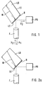
- FIG. 1 shows an optical transmitter and receiver module according to the invention for bidirectional transmission with wavelength division multiplexing.
- a laser diode LD is provided for transmitting light of a first wavelength ⁇ 1 .
- a reception diode PD is also provided for receiving light of a second wavelength ⁇ 2 .
- an optical fiber end F is provided, which serves to transmit light of the two predetermined wavelengths ⁇ 1 and ⁇ 2 .
- the laser diode LD is, for example, a DFB or a DBR laser, the function of which is not based on the reflection of the Light based on the laser end faces.
- the position of the waveguide W in the laser diode LD is indicated by a dash.
- the direction of the waveguide in the laser diode LD is therefore parallel to the position of the waveguide W.
- the laser side surfaces LS run parallel to the waveguide W.
- a light-emitting laser end surface LE is not perpendicular to the direction of the waveguide W and thus to the direction of the waveguide in the laser diode LD.
- the end surface LE and the direction of the wave guide are at an angle other than 90 °.
- This laser end surface LE, which is inclined to the direction of the wave guide has a wavelength-selective coating B.
- the coating B is transparent to light of the wavelength ⁇ 1 and reflective to light of the wavelength ⁇ 2 .
- Light from the fiber end F of the wavelength ⁇ 2 is reflected on the coating B and falls on the receiving diode PD.
- Light from the laser diode LD with the wavelength ⁇ 1 is transmitted through the wavelength-selective coating B, is refracted when it emerges from the coating and is then coupled into the end of the optical waveguide.
- the waveguide W is arranged inclined to the side faces in a rectangular laser diode (FIG. 2a). It is also possible that the laser diode is diamond-shaped in section and the waveguide is arranged parallel to the side surfaces of the laser diode (FIG. 2b).
- the angle ⁇ between incident light and reflected light can also be chosen to be not equal to 90 °. It is not necessary that both light-emitting laser end faces are inclined toward the waveguide W.
- the light-emitting end surface which is not used, can be any angle ⁇ to the perpendicular on the side surface of the laser diodes LD exhibit.
- the side surface of the laser diode and the fiber axis can be arranged parallel to one another (FIG. 2c).
- FIG. 2d shows an arrangement in which the angle between the beam path from the fiber F to the laser diode LD and from the laser diode LD to the receiving diode PD is 90 °. Since the position of the waveguide in the laser diode and the angle of the laser end face LE can be freely selected, the angle ⁇ can be determined as desired.
- FIG. 3 shows an arrangement according to FIG. 2d, which is introduced into a silicon carrier T with anisotropically etched V-grooves and depressions.
- a ball lens K1, K2 is provided between the receiving diode PD and the optical waveguide F and the laser diode LD, with which a beam adaptation and focusing is carried out.
- the receiving diode PD is not mounted in a recess, but on the silicon carrier T.
- a section from A to B is shown, which shows that the light beam falling on the photodiode is reflected on the inclined end face of the V-groove and falls on the photodiode.
- One side surface of the laser diode is arranged parallel to the optical waveguide F. Due to the anisotropic etching technique, stops in the silicon carrier T are etched, which are parallel to this side surface and which simplify the adjustment of the laser diode. This means that the position of the laser diode is only fixed in one direction.
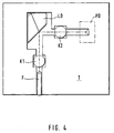
- FIG. 4 shows a corresponding arrangement in which the second light-emitting laser end face is at a right angle to the side face of the laser. Since stops on the silicon carrier T also have a right angle to one another when they have been anisotropically etched, it is thereby possible to adjust the laser diode LD in both directions with the aid of these stops.
- a problem with the exemplary embodiments described so far is that a beam transformation is required between the laser diode and the fiber because of the different beam characteristics of the laser diode and the single-mode fiber.
- the beam guided in the fiber must be transformed so that it has approximately the same divergence as the laser on the end face of the laser.
- the received beam reflected on the laser face will therefore have a very large divergence.
- For an effective coupling of a photodiode it must either have a very large active area, which has a disadvantageous effect on the achievable cutoff frequency, or the photodiode must sit very close to the laser end face, which results in space problems and problems with electrical crosstalk, or it must also have a coupling optics be used. This problem does not occur in the following exemplary embodiment (FIG. 5).
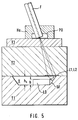
- the laser diode LD is seated on a recess anisotropically etched in a silicon carrier T1 with a flat bottom and side surfaces SF inclined by 54.7 °, at least one of which is mirrored.
- the light-emitting end surface of the laser ends as close as possible in front of a mirrored side surface of the depression.
- the received light beam emerging from the fiber strikes the laser end face after passing through the lens L1 and after reflection on the side face SF and is reflected there at the angle - ⁇ . After a further reflection on the side face SF, it passes through the lens L2 and is focused into the receiving photodiode PD.
- the angle ⁇ must be at least as large as the horizontal far field angle of the laser in order to separate the transmit and To reach the receiving beam.
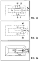
- Another carrier T2 with two lenses is attached in a plane parallel to the surface of the silicon carrier above the silicon carrier with the recess V for receiving the laser (FIG. 6b).
- These lenses can be, for example, microstructured Fresnel lenses on a support made of glass or silicon or another suitable material. Holographically produced lenses are also possible. Lenses that can be produced in silicon by known dry etching processes are also suitable here.
- the lenses are symmetrical about a plane of symmetry E s , which contains the surface normal of the laser end face, the light exit window of the laser and the surface normal of the silicon carrier.
- This plane is the yz plane of a right-angled coordinate system, the z axis of which is the surface normal of the laser end face and the y axis of which is the surface normal of the silicon substrate.
- the x-axis lies in the active layer of the laser.
- One lens lies in the beam path of the laser or the received signal emerging from the fiber and the other lies in the beam path of the reflected signal on the laser end face Received signal.
- the light exit window of the laser is imaged on the two image points B1 and B2, which have a distance b in the beam direction from the respective lenses (FIG. 6c).
- the fiber and the photodiode are mounted above the lens plane.
- the image point for the fiber is, due to the two imaging with M and 1 / M, just as large as the mode field diameter of the fiber, which is 10 ⁇ m with standard single mode fibers.
- Mounting tolerances of the laser relative to the lens carrier plate have a similar effect on the position of the two pixels B 1 and B 2 and are enlarged in accordance with the magnification ratio M of the figure.
- the misalignment of the laser has no effect on the mutual distance d b of the two pixels. This distance is determined by the distance between the lens centers d 1 and to a small extent by the object and image width.
- the adjustment of the fiber which is necessary to compensate for the assembly tolerances of the laser, also simultaneously adjusts the photodiode with almost the same accuracy. Because of this and because of the small size of the beam waist in the pixel B 2 , a photodiode with a very small diameter can be used the active zone, which allows very high cut-off frequencies in the GHz range. With a diameter of the active zone of the photodiode of 30 ⁇ m, there are still lateral tolerances to the position of the fiber core of ⁇ 10 ⁇ m for the mounting of the photodiode on the common carrier, which can still be achieved with passive mounting with the aid of alignment marks.
- the fiber Since the beam path is inclined relative to the normal to the substrate surface by the directional angles ⁇ zy and ⁇ xy , either the fiber must also be inclined in this way, or this inclination must be compensated for by mounting the fiber vertically by means of a corresponding grinding angle of the fiber end face. The latter would have the advantage of avoiding harmful back reflections from the face of the fiber onto the laser. Horizontal mounting of the fiber, for example in an anisotropically etched silicon carrier with a V-groove for receiving the fiber, is also possible. The received and transmitted light bundle is then deflected on the mirrored end face of the fiber V-groove (see FIG. 7).
- a second proposal for beam guidance is shown in FIG. 8.
- the laser chip is also mounted on the bottom of a recess.
- the laser does not sit here with its edge parallel to the foot edge of one side surface of the recess, but in front of a corner of two adjacent mirrored side surfaces, so that the transmitted light beam hits one side surface and the reception light beam hits the other side surface.
- the two light beams of the transmission and reception beam reflected on the side surfaces intersect.
- a single lens for both beams is placed in the crossing point. Since both beams emanate from different mirror images of the laser, corresponding to the reflection on the different side surfaces also their pixels despite the image with only one lens at different locations B 1 and B 2 .
- the assembly and adjustment of fiber and photodiode is carried out in these pixels, as stated in proposal 1.
Landscapes
- Physics & Mathematics (AREA)
- General Physics & Mathematics (AREA)
- Optics & Photonics (AREA)
- Condensed Matter Physics & Semiconductors (AREA)
- Electromagnetism (AREA)
- Optical Couplings Of Light Guides (AREA)
Abstract
Description
Die Erfindung betrifft ein optisches Sende- und Empfangsmodul für bidirektionale Übertragung mit Wellenlängenmultiplex mit einer Laserdiode zum Senden von Licht einer ersten Wellenlänge, mit einer Empfangsdiode zum Empfangen von Licht einer zweiten Wellenlänge und mit einem Lichtwellenleiterende zum Übertragen von Licht der beiden vorgegebenen Wellenlängen.The invention relates to an optical transmission and reception module for bidirectional transmission with wavelength division multiplexing with a laser diode for transmitting light of a first wavelength, with a reception diode for receiving light of a second wavelength and with an optical waveguide end for transmitting light of the two predetermined wavelengths.
Aus der DE 38 01 764 ist ein mikrooptischer Multiplexer bekannt. Auf einem Siliziumsubstrat sind mit Hilfe der anisotropen Ätztechnik V-Nuten und Vertiefungen hergestellt, in die Kugellinsen, Glasfasern und Filterplättchen eingelegt werden können. Ein optisches Sende- und Empfangsmodul für bidirektionale Übertragung mit Wellenlängenmultiplex besteht bei einer nach diesem Stand der Technik ausgeführten Anordnung aus einer Laserdiode, einem Filterplättchen, einer Empfangsdiode und einem Lichtwellenleiterende, die in entsprechende Vertiefungen in dem Siliziumträger eingelegt sind. Zur Strahlanpassung sind zwischen den einzelnen Komponenten und dem Filterplättchen Linsen vorgesehen. Die Herstellung der Halterungen für das Filterplättchen ist sehr aufwendig.A micro-optical multiplexer is known from DE 38 01 764. Using anisotropic etching technology, V-grooves and recesses are made on a silicon substrate, into which ball lenses, glass fibers and filter plates can be inserted. An optical transmission and reception module for bidirectional transmission with wavelength division multiplexing in an arrangement designed according to this prior art consists of a laser diode, a filter plate, a reception diode and an optical fiber end, which are inserted into corresponding recesses in the silicon carrier. Lenses are provided between the individual components and the filter plate for beam adaptation. The manufacture of the holders for the filter plate is very complex.
Ausgehend von diesem Stand der Technik ist es Aufgabe der Erfindung, einen vereinfachten Aufbau für ein optisches Sende- und Empfangsmodul für bidirektionale Übertragung mit Wellenlängenmultiplex anzugeben. Die Aufgabe wird durch eine Anordnung mit den Merkmalen des Patentanspruches 1 gelöst. Vorteilhafte Weiterbildungen sind in den Unteransprüchen angegeben.Based on this prior art, it is an object of the invention to provide a simplified structure for an optical transmitter and receiver module for bidirectional transmission with wavelength division multiplexing. The object is achieved by an arrangement with the features of
Durch den Einsatz einer Laserdiode mit einer wellenlängenselektiven Beschichtung in einem optischen Sende- und Empfangsmodul für bidirektionale Übertragung mit Wellenlängenmultiplex ergibt sich der Vorteil, daß der Einsatz einzelner Filterplättchen entfällt und daß diese somit auch nicht in Halterungen fixiert und justiert werden müssen. Die an der Laserdiode vorgesehene Beschichtung kann bereits bei der Herstellung der Laserdiode mit den bekannten Verfahren der Halbleitertechnik vorgenommen werden. Eine Beschichtung der lichtemittierenden Laserendfläche ist ohnehin zur Passivierung der Laserendfläche erforderlich. Zur Wellenlängenselektion und räumlichen Trennung ist es notwendig, daß die Richtung der Wellenführung im Laser und die lichtemittierende Laserendfläche in einem von 90° abweichenden Winkel zueinander stehen. Daher muß ein Laser zum Einsatz kommen, dessen Funktion als Laser nicht auf der Reflexion an den Kristallendflächen beruht. Dieses Kriterium wird beispielsweise von DFB- oder DBR-Lasern erfüllt. Bei diesen Lasern ist es sogar vorteilhaft, wenn das Licht an den Kristallendflächen nicht zurück in den Wellenleiter reflektiert wird.The use of a laser diode with a wavelength-selective coating in an optical transmitter and receiver module for bidirectional transmission with wavelength division multiplex results in the advantage that there is no need to use individual filter plates and that they therefore do not have to be fixed and adjusted in holders. The coating provided on the laser diode can already be carried out during the manufacture of the laser diode using the known methods of semiconductor technology. A coating of the light-emitting laser end surface is required anyway in order to passivate the laser end surface. For wavelength selection and spatial separation, it is necessary that the direction of the wave guide in the laser and the light-emitting laser end face are at an angle other than 90 °. Therefore, a laser must be used whose function as a laser is not based on the reflection at the crystal end faces. This criterion is met, for example, by DFB or DBR lasers. With these lasers, it is even advantageous if the light at the crystal end faces is not reflected back into the waveguide.
Für die vorliegende Erfindung ist es erforderlich, daß mindestens eine lichtemittierende Endfläche in einem bestimmten Winkel zum Lichtwellenleiterende und zur Empfangsdiode sowie zur Richtung der Wellenführung im Laser angeordnet wird. Die Winkel zwischen dieser geneigten lichtemittierenden Laserendfläche und den Seitenflächen bzw. der zweiten Laserendfläche können so gewählt werden, wie es fertigungstechnisch am günstigsten ist, zum Beispiel zur Ausnutzung von Kristallebenen. Es ist besonders vorteilhaft, die Seitenflächen derart zu wählen, daß sie parallel zu den Seitenflächen von anisotrop geätzten Führungsnuten in einem Siliziumträger angeordnet werden können. Dies erspart zusätzliche Justierschritte bei der Montage der Laserdiode auf einem Siliziumträger.For the present invention, it is necessary that at least one light-emitting end surface is arranged at a certain angle to the end of the optical waveguide and to the receiving diode and to the direction of the wave guide in the laser. The angles between this inclined light-emitting laser end face and the side faces or The second laser end surface can be selected in such a way that it is the most economical in terms of production technology, for example for the utilization of crystal planes. It is particularly advantageous to choose the side surfaces in such a way that they can be arranged in a silicon carrier parallel to the side surfaces of anisotropically etched guide grooves. This saves additional adjustment steps when mounting the laser diode on a silicon carrier.
Ausführungsbeispiele der Erfindung werden anhand der Zeichnungen erläutert. Es zeigen:
Figur 1 ein optisches Sende- und Empfangsmodul,- Figuren 2a bis d verschiedene Ausgestaltungen der Laserdiode mit wellenlängenselektivem Filter,
Figur 3 einen Aufbau auf einem Silizium-Träger mit geätzten Vertiefungen,- Figur 4 einen weiteren Aufbau auf einem Silizium-Träger mit geätzten Vertiefungen,
- Figur 5 einen Aufbau mit mehreren übereinanderliegenden Trägern,
- Figuren 6a bis c verschiedene Schnitte durch einen Aufbau gemäß Figur 5,
- Figur 7 eine zusätzliche Variante zur Anordnung gemäß Figur 5 mit einer horizontal angeordneten Faser,
- Figur 8 eine weitere Anordnungsmöglichkeit für die Laserdiode.
- FIG. 1 shows an optical transmission and reception module,
- FIGS. 2a to d show different configurations of the laser diode with a wavelength-selective filter,
- FIG. 3 shows a structure on a silicon carrier with etched depressions,
- FIG. 4 shows a further structure on a silicon carrier with etched depressions,
- FIG. 5 shows a structure with a plurality of supports lying one above the other,
- 6a to c show different sections through a structure according to FIG. 5,
- FIG. 7 shows an additional variant for the arrangement according to FIG. 5 with a horizontally arranged fiber,
- Figure 8 shows another arrangement option for the laser diode.
Figur 1 zeigt ein erfindungsgemäßes optisches Sende- und Empfangsmodul für bidirektionale Übertragung mit Wellenlängenmultiplex. Es ist eine Laserdiode LD vorgesehen zum Senden von Licht einer ersten Wellenlänge λ1. Weiter ist eine Empfangsdiode PD zum Empfangen von Licht einer zweiten Wellenlänge λ2 vorgesehen. Außerdem ist ein Lichtwellenleiterende F vorgesehen, daß zum Übertragen von Licht der beiden vorgegebenen Wellenlängen λ1 und λ2 dient. Die Laserdiode LD ist beispielsweise ein DFB- oder ein DBR-Laser, dessen Funktion nicht auf der Reflexion des Lichts an den Laserendflächen beruht. In Figur 1 ist die Lage des Wellenleiters W in der Laserdiode LD durch einen Strich angedeutet. Die Richtung der Wellenführung in der Laserdiode LD liegt also parallel zur Lage des Wellenleiters W. Die Laserseitenflächen LS verlaufen parallel zum Wellenleiter W. Eine lichtemittierende Laserendfläche LE ist nicht senkrecht zur Richtung des Wellenleiters W und somit zur Richtung der Wellenführung in der Laserdiode LD angeordnet. Die Endfläche LE und die Richtung der Wellenführung stehen in einem von 90° abweichenden Winkel zueinander. Diese zur Richtung der Wellenführung geneigte Laserendfläche LE weist eine wellenlängenselektive Beschichtung B auf. Die Beschichtung B ist für Licht der Wellenlänge λ1 durchlässig und für Licht der Wellenlänge λ2 reflektierend. Licht aus dem Lichtwellenleiterende F der Wellenlänge λ2 wird an der Beschichtung B reflektiert und fällt auf die Empfangsdiode PD. Licht aus der Laserdiode LD der Wellenlänge λ1 wird durch die wellenlängenselektive Beschichtung B hindurchgelassen, wird beim Austritt aus der Beschichtung gebrochen und dann in das Lichtwellenleiterende eingekoppelt.FIG. 1 shows an optical transmitter and receiver module according to the invention for bidirectional transmission with wavelength division multiplexing. A laser diode LD is provided for transmitting light of a first wavelength λ 1 . A reception diode PD is also provided for receiving light of a second wavelength λ 2 . In addition, an optical fiber end F is provided, which serves to transmit light of the two predetermined wavelengths λ 1 and λ 2 . The laser diode LD is, for example, a DFB or a DBR laser, the function of which is not based on the reflection of the Light based on the laser end faces. In Figure 1, the position of the waveguide W in the laser diode LD is indicated by a dash. The direction of the waveguide in the laser diode LD is therefore parallel to the position of the waveguide W. The laser side surfaces LS run parallel to the waveguide W. A light-emitting laser end surface LE is not perpendicular to the direction of the waveguide W and thus to the direction of the waveguide in the laser diode LD. The end surface LE and the direction of the wave guide are at an angle other than 90 °. This laser end surface LE, which is inclined to the direction of the wave guide, has a wavelength-selective coating B. The coating B is transparent to light of the wavelength λ 1 and reflective to light of the wavelength λ 2 . Light from the fiber end F of the wavelength λ 2 is reflected on the coating B and falls on the receiving diode PD. Light from the laser diode LD with the wavelength λ 1 is transmitted through the wavelength-selective coating B, is refracted when it emerges from the coating and is then coupled into the end of the optical waveguide.
Es gibt eine ganze Reihe von Möglichkeiten, wie eine Laserdiode zum Einsatz in einem erfindungsgemäßen optischen Sende- und Empfangsmodul aussehen kann. Es ist beispielsweise möglich, daß in einer an sich quaderförmigen Laserdiode der Wellenleiter W gegen die Seitenflächen geneigt angeordnet ist (Figur 2a). Es ist auch möglich, daß die Laserdiode im Schnitt rautenförmig ist und der Wellenleiter parallel zu den Seitenflächen der Laserdiode angeordnet ist (Figur 2b). Der Winkel α zwischen einfallendem Licht und reflektiertem Licht kann dabei auch ungleich 90° gewählt werden. Es ist nicht notwendig, daß beide lichtemittierenden Laserendflächen gegen den Wellenleiter W geneigt sind. Die lichtemittierende Endfläche, die nicht ausgenutzt wird, kann einen beliebigen Winkel β zur Senkrechten auf der Seitenfläche der Laserdioden LD aufweisen. Für die Montage der Laserdiode und der Faser auf einem Siliziumträger ist es von besonderem Vorteil, wenn die Seitenfläche der Laserdiode und die Faserachse parallel zueinander angeordnet werden können (Figur 2c). Figur 2d zeigt eine Anordnung, bei der der Winkel zwischen dem Strahlengang von der Faser F zur Laserdiode LD und von der Laserdiode LD zur Empfangsdiode PD 90° beträgt. Da die Lage des Wellenleiters in der Laserdiode und der Winkel der Laserendfläche LE frei wählbar sind, kann der Winkel α beliebig bestimmt werden.There are a whole range of possibilities of what a laser diode for use in an optical transmitter and receiver module according to the invention can look like. It is possible, for example, for the waveguide W to be arranged inclined to the side faces in a rectangular laser diode (FIG. 2a). It is also possible that the laser diode is diamond-shaped in section and the waveguide is arranged parallel to the side surfaces of the laser diode (FIG. 2b). The angle α between incident light and reflected light can also be chosen to be not equal to 90 °. It is not necessary that both light-emitting laser end faces are inclined toward the waveguide W. The light-emitting end surface, which is not used, can be any angle β to the perpendicular on the side surface of the laser diodes LD exhibit. For the assembly of the laser diode and the fiber on a silicon carrier, it is particularly advantageous if the side surface of the laser diode and the fiber axis can be arranged parallel to one another (FIG. 2c). FIG. 2d shows an arrangement in which the angle between the beam path from the fiber F to the laser diode LD and from the laser diode LD to the receiving diode PD is 90 °. Since the position of the waveguide in the laser diode and the angle of the laser end face LE can be freely selected, the angle α can be determined as desired.
Figur 3 zeigt eine Anordnung gemäß Figur 2d, die in einen Siliziumträger T mit anisotrop geätzten V-Nuten und Vertiefungen eingebracht ist. Jeweils zwischen der Empfangsdiode PD und dem Lichtwellenleiter F und der Laserdiode LD ist eine Kugellinse K1, K2 vorgesehen, mit der eine Strahlanpassung und Fokussierung durchgeführt wird. Die Empfangsdiode PD ist nicht in einer Vertiefung, sondern auf dem Silizium-Träger T montiert. In der unteren kleinen Zeichnung ist ein Schnitt von A nach B dargestellt, der zeigt, daß der auf die Fotodiode fallende Lichtstrahl an der geneigten Stirnfläche der V-Nut reflektiert wird und auf die Fotodiode fällt. Eine Seitenfläche der Laserdiode ist parallel zum Lichtwellenleiter F angeordnet. Aufgrund der anisotropen Ätztechnik sind Anschläge im Silizium-Träger T geätzt, die zu dieser Seitenfläche parallel sind und die die Justage der Laserdiode vereinfachen. Dadurch ist die Lage der Laserdiode jedoch nur in einer Richtung festgelegt.FIG. 3 shows an arrangement according to FIG. 2d, which is introduced into a silicon carrier T with anisotropically etched V-grooves and depressions. A ball lens K1, K2 is provided between the receiving diode PD and the optical waveguide F and the laser diode LD, with which a beam adaptation and focusing is carried out. The receiving diode PD is not mounted in a recess, but on the silicon carrier T. In the lower small drawing a section from A to B is shown, which shows that the light beam falling on the photodiode is reflected on the inclined end face of the V-groove and falls on the photodiode. One side surface of the laser diode is arranged parallel to the optical waveguide F. Due to the anisotropic etching technique, stops in the silicon carrier T are etched, which are parallel to this side surface and which simplify the adjustment of the laser diode. This means that the position of the laser diode is only fixed in one direction.
Figur 4 zeigt eine entsprechende Anordnung in der die zweite lichtemittierende Laserendfläche in einem rechten Winkel zur Seitenfläche des Lasers steht. Da auch Anschläge auf dem Silizium-Träger T einen rechten Winkel zueinander aufweisen, wenn sie anisotrop geätzt wurden, ist es dadurch möglich die Laserdiode LD in beiden Richtungen mit Hilfe dieser Anschläge zu justieren.FIG. 4 shows a corresponding arrangement in which the second light-emitting laser end face is at a right angle to the side face of the laser. Since stops on the silicon carrier T also have a right angle to one another when they have been anisotropically etched, it is thereby possible to adjust the laser diode LD in both directions with the aid of these stops.
Ein Problem der bisher beschriebenen Ausführungsbeispiele besteht darin, daß zwischen der Laserdiode und der Faser wegen der unterschiedlichen Strahlcharakteristiken von Laserdiode und Einmodenfaser eine Strahltransformation erforderlich ist. Der in der Faser geführte Strahl muß dabei so transformiert werden, daß er an der Stirnfläche des Lasers etwa die gleiche Divergenz wie der Laser besitzt. Der an der Laserstirnfläche reflektierte Empfangsstrahl wird also eine sehr große Divergenz besitzen. Für eine effektive Ankopplung einer Photodiode muß diese entweder eine sehr große aktive Fläche besitzen, was sich nachteilig auf die erreichbare Grenzfrequenz auswirkt, oder die Photodiode muß sehr dicht an der Laserstirnfläche sitzen, was Platzprobleme und Probleme mit elektrischem Übersprechen ergibt oder es muß ebenfalls eine Koppeloptik verwendet werden. Beim folgenden Ausführungsbeispiel (Figur 5) tritt dieses Problem nicht auf.A problem with the exemplary embodiments described so far is that a beam transformation is required between the laser diode and the fiber because of the different beam characteristics of the laser diode and the single-mode fiber. The beam guided in the fiber must be transformed so that it has approximately the same divergence as the laser on the end face of the laser. The received beam reflected on the laser face will therefore have a very large divergence. For an effective coupling of a photodiode, it must either have a very large active area, which has a disadvantageous effect on the achievable cutoff frequency, or the photodiode must sit very close to the laser end face, which results in space problems and problems with electrical crosstalk, or it must also have a coupling optics be used. This problem does not occur in the following exemplary embodiment (FIG. 5).
Die Laserdiode LD sitzt an einer in einem Siliziumträger T1 anisotrop geätzten Vertiefung mit ebenem Boden und um 54,7° geneigten Seitenflächen SF, von denen mindestens eine verspiegelt ist. Die lichtemittierende Stirnfläche des Lasers endet so nah wie möglich vor einer verspiegelten Seitenfläche der Vertiefung. Das aus dem Laser austretende Lichtbündel, dessen Mittenstrahl erfindungsgemäß nicht in Richtung der Flächennormalen der Laserstirnseite austritt, sondern mit dieser einen horizontalen Winkel α einschließt, wird an der geneigten Stirnseite schräg nach oben und vorn reflektiert. Das aus der Faser austretende Empfangslichtbündel trifft nach Durchlaufen der Linse L1 und nach Reflexion an der Seitenfläche SF auf die Laserstirnfläche und wird dort unter dem Winkel -α reflektiert. Nach einer weiteren Reflexion an der Seitenfläche SF durchläuft es die Linse L2 und wird in die Empfangs-Photodiode PD fokussiert. Der Winkel α muß dabei mindestens so groß sein wie der horizontale Fernfeldwinkel des Lasers, um eine ausreichende Trennung von Sende- und Empfangsstrahl zu erreichen. Bei einem typischen Laser mit einem Fernfeld von 25° (FWHM) in horizontaler und 35° (FWHM) in vertikaler Richtung erhält man aus




Die Brennweite f der beiden Linsen errechnet sich nach der Linsengleichung zu

Beispielhaft soll für einen Laser mit dem oben angeführten Fernfeld und einer Dicke von 100µm, dessen aktiver Zone auf seiner Oberseite in einer Höhe h = 95µm über der Chipauflage liegt, und der mit seinem unteren Chiprand unmittelbar an den Fuß der Seitenwand stößt die erforderliche Geometrie berechnet werden. Der Lichtweg g1 des Mittenstrahls vom Lichtaustrittsfenster des Lasers bis zur Seitenwand ist
Damit das ganze Laserlichtbündel die reflektierende Seitenfläche treffen kann, muß diese bis zu einer Höhe


Die Länge g2 des Mittenstrahls von der Reflexionsstelle an der Seitenwand bis zur Unterseite des Linsensträgers ist
Zur gesamten Gegenstandweite kommt noch der Lichtweg g3 von der Unterseite des Linsenträgers bis zum Linsenmittelpunkt hinzu. Dieser zusätzliche Lichtweg hängt von der Art der verwendeten Linse ab. Bei der Fresnellinse oder einer holographischen Linse ist g3 = 0. Die Gegenstandsweite ist dann
Ist zur Strahltransformation ein Vergrößerungsverhältnis von M = 4,5 erforderlich, so ist die erforderliche Brennweite der Linse f = 123µm. Die Bildweite ist dann 676µm. Dieses Zahlenbeispiel bezieht sich auf die Minimalkonfiguration von Gegenstands- , Bild- und Brennweite für den oben beschriebenen Laser. Größere Werte können entsprechend der Möglichkeiten der eingesetzten Linse ebenfalls verwendet werden.If a magnification ratio of M = 4.5 is required for beam transformation, the required focal length of the lens is f = 123 µm. The image width is then 676µm. This Numerical example refers to the minimal configuration of object, image and focal length for the laser described above. Larger values can also be used depending on the possibilities of the lens used.
In der Bildebene, die im Abstand

Der Bildpunkt für die Faser ist infolge der zweimaligen Abbildung mit M und 1/M gerade so groß wie der Modenfelddurchmesser der Faser, der bei Standardeinmodenfasern bei 10µm liegt. Montagetoleranzen des Lasers relativ zu der Linsenträgerplatte wirken sich gleichartig auf die Lage der beiden Bildpunkte B1 und B2 aus und werden entsprechend dem Vergrößerungsverhältnis M der Abbildung vergrößert. Auf den gegenseitigen Abstand db beider Bildpunkte wirkt sich die Dejustage des Lasers jedoch nicht aus. Dieser Abstand wird durch den Abstand der Linsenmitten d1 und in geringem Maß von der Gegenstands- und Bildweite bestimmt. Bei gleichzeitiger Erzeugung beider Linsen in einem photolithografischen Prozeß kann der Linsenabstand sehr genau eingehalten werden. Bringt man den Halter Ha für die Faser und die Photodiode auf einen gemeinsamen Träger T3, so wird bei der Justage der Faser, die zum Ausgleich der Montagetoleranzen des Lasers erforderlich ist, gleichzeitig auch die Photodiode mit nahezu der gleichen Genauigkeit mitjustiert. Dadurch und wegen der geringen Größe der Strahltaille im Bildpunkt B2 läßt sich eine Photodiode mit einem sehr kleinen Durchmesser der aktiven Zone einsetzen, womit sehr hohe Grenzfrequenzen im GHz-Bereich möglich sind. Bei einem Durchmesser der aktiven Zone der Photodiode von 30µm bleiben für die Montage der Photodiode auf dem gemeinsamen Träger noch laterale Toleranzen zur Position des Faserkerns von ± 10µm, die noch mit einer passiven Montage mit Hilfe von Justagemarken erreicht werden können.The image point for the fiber is, due to the two imaging with M and 1 / M, just as large as the mode field diameter of the fiber, which is 10 µm with standard single mode fibers. Mounting tolerances of the laser relative to the lens carrier plate have a similar effect on the position of the two pixels B 1 and B 2 and are enlarged in accordance with the magnification ratio M of the figure. However, the misalignment of the laser has no effect on the mutual distance d b of the two pixels. This distance is determined by the distance between the lens centers d 1 and to a small extent by the object and image width. When both lenses are produced simultaneously in a photolithographic process, the lens spacing can be maintained very precisely. If the holder Ha for the fiber and the photodiode are placed on a common carrier T3, the adjustment of the fiber, which is necessary to compensate for the assembly tolerances of the laser, also simultaneously adjusts the photodiode with almost the same accuracy. Because of this and because of the small size of the beam waist in the pixel B 2 , a photodiode with a very small diameter can be used the active zone, which allows very high cut-off frequencies in the GHz range. With a diameter of the active zone of the photodiode of 30 µm, there are still lateral tolerances to the position of the fiber core of ± 10 µm for the mounting of the photodiode on the common carrier, which can still be achieved with passive mounting with the aid of alignment marks.
Da der Strahlverlauf gegenüber der Normalen der Substratoberfläche um die Richtungswinkel γzy und γxy geneigt ist, muß entweder die Faser in ihrer Aufnahme ebenfalls so geneigt sein oder diese Neigung muß bei senkrechter Montage der Faser durch einen entsprechenden Schliffwinkel der Faserstirnfläche kompensiert werden. Letzteres hätte den Vorteil, daß dabei schädliche Rückreflexionen von der Faserstirnfläche auf den Laser vermieden werden. Auch eine horizontale Montage der Faser, beispielsweise in einem anisotrop geätzten Siliziumträger mit einer V-Nut zur Aufnahme der Faser, ist möglich. Das Empfangs- und Sendelichtbündel wird dann an der verspiegelten Stirnfläche der Faser-V-Nut umgelenkt (siehe Figur 7).Since the beam path is inclined relative to the normal to the substrate surface by the directional angles γ zy and γ xy , either the fiber must also be inclined in this way, or this inclination must be compensated for by mounting the fiber vertically by means of a corresponding grinding angle of the fiber end face. The latter would have the advantage of avoiding harmful back reflections from the face of the fiber onto the laser. Horizontal mounting of the fiber, for example in an anisotropically etched silicon carrier with a V-groove for receiving the fiber, is also possible. The received and transmitted light bundle is then deflected on the mirrored end face of the fiber V-groove (see FIG. 7).
Ein zweiter Vorschlag zur Strahlführung ist in der Figur 8 dargestellt. Hier ist der Laserchip ebenfalls auf dem Boden einer Vertiefung montiert. Im Unterschied zum ersten Vorschlag sitzt der Laser hier nicht mit seiner Kante parallel zur Fußkante einer Seitenfläche der Vertiefung sondern vor einer Ecke zweier benachbarter verspiegelter Seitenflächen, so daß das Sendelichtbündel die eine Seitenfläche und das Empfangslichtbündel die andere Seitenfläche trifft. Die beiden an den Seitenflächen reflektierten Lichtbündel des Sende- und Empfangsstrahls kreuzen sich. In den Kreuzungspunkt wird eine einzelne Linse für beiden Strahlen angebracht. Da beide Strahlen von verschiedenen Spiegelbildern des Lasers, entsprechend der Reflexion an den verschiedenen Seitenflächen, ausgehen, sind auch ihre Bildpunkte trotz der Abbildung mit nur einer Linse an verschiedenen Orten B1 und B2. In diesen Bildpunkten wird, wie im Vorschlag 1 ausgeführt, die Montage und Justage von Faser und Photodiode durchgeführt.A second proposal for beam guidance is shown in FIG. 8. Here the laser chip is also mounted on the bottom of a recess. In contrast to the first proposal, the laser does not sit here with its edge parallel to the foot edge of one side surface of the recess, but in front of a corner of two adjacent mirrored side surfaces, so that the transmitted light beam hits one side surface and the reception light beam hits the other side surface. The two light beams of the transmission and reception beam reflected on the side surfaces intersect. A single lens for both beams is placed in the crossing point. Since both beams emanate from different mirror images of the laser, corresponding to the reflection on the different side surfaces also their pixels despite the image with only one lens at different locations B 1 and B 2 . The assembly and adjustment of fiber and photodiode is carried out in these pixels, as stated in
Claims (10)
auf dem Siliziumträger (T) ein weiterer Träger vorgesehen ist, der zwei Linsen in den Strahlengang einbringt.Optical transmission and reception module according to claim 6, characterized in that
a further carrier is provided on the silicon carrier (T), which introduces two lenses into the beam path.
die Linsen mikrostrukturierte Fresnellinsen auf einem Träger aus Glas oder Silizium sind.Optical transmission and reception module according to claim 7, characterized in that
the lenses are microstructured Fresnel lenses on a support made of glass or silicon.
die Linsen holographisch erzeugte Linsen sind.Optical transmission and reception module according to claim 7, characterized in that
the lenses are holographically produced lenses.
die Linsen durch Trockenätzverfahren in Silizium erzeugte Linsen sind.Optical transmission and reception module according to claim 7, characterized in that
the lenses are lenses produced in silicon by dry etching processes.
Priority Applications (1)
| Application Number | Priority Date | Filing Date | Title |
|---|---|---|---|
| EP96107309A EP0806684A1 (en) | 1996-05-09 | 1996-05-09 | Optical transmitting and receiving module |
Applications Claiming Priority (1)
| Application Number | Priority Date | Filing Date | Title |
|---|---|---|---|
| EP96107309A EP0806684A1 (en) | 1996-05-09 | 1996-05-09 | Optical transmitting and receiving module |
Publications (1)
| Publication Number | Publication Date |
|---|---|
| EP0806684A1 true EP0806684A1 (en) | 1997-11-12 |
Family
ID=8222765
Family Applications (1)
| Application Number | Title | Priority Date | Filing Date |
|---|---|---|---|
| EP96107309A Withdrawn EP0806684A1 (en) | 1996-05-09 | 1996-05-09 | Optical transmitting and receiving module |
Country Status (1)
| Country | Link |
|---|---|
| EP (1) | EP0806684A1 (en) |
Citations (5)
| Publication number | Priority date | Publication date | Assignee | Title |
|---|---|---|---|---|
| DE3801764A1 (en) * | 1988-01-22 | 1989-08-03 | Ant Nachrichtentech | WAVELENGTH MULTIPLEXER OR DEMULTIPLEXER, AND METHOD FOR PRODUCING THE WAVELENGTH MULTIPLEXER OR DEMULTIPLEXER |
| JPH01238082A (en) * | 1988-03-18 | 1989-09-22 | Nippon Telegr & Teleph Corp <Ntt> | Semiconductor laser |
| DE9319378U1 (en) * | 1993-12-16 | 1994-02-17 | Siemens AG, 80333 München | Combined sending and receiving station for optical message transmission |
| EP0631163A1 (en) * | 1993-05-17 | 1994-12-28 | Siemens Aktiengesellschaft | Bidirectional optical transceiver |
| DE4407451C1 (en) * | 1994-03-05 | 1995-05-04 | Ant Nachrichtentech | Wavelength duplexer |
-
1996
- 1996-05-09 EP EP96107309A patent/EP0806684A1/en not_active Withdrawn
Patent Citations (5)
| Publication number | Priority date | Publication date | Assignee | Title |
|---|---|---|---|---|
| DE3801764A1 (en) * | 1988-01-22 | 1989-08-03 | Ant Nachrichtentech | WAVELENGTH MULTIPLEXER OR DEMULTIPLEXER, AND METHOD FOR PRODUCING THE WAVELENGTH MULTIPLEXER OR DEMULTIPLEXER |
| JPH01238082A (en) * | 1988-03-18 | 1989-09-22 | Nippon Telegr & Teleph Corp <Ntt> | Semiconductor laser |
| EP0631163A1 (en) * | 1993-05-17 | 1994-12-28 | Siemens Aktiengesellschaft | Bidirectional optical transceiver |
| DE9319378U1 (en) * | 1993-12-16 | 1994-02-17 | Siemens AG, 80333 München | Combined sending and receiving station for optical message transmission |
| DE4407451C1 (en) * | 1994-03-05 | 1995-05-04 | Ant Nachrichtentech | Wavelength duplexer |
Non-Patent Citations (3)
| Title |
|---|
| BUUS J ET AL: "REFLECTIVITY OF COATED AND TILTED SEMICONDUCTOR FACETS", IEEE JOURNAL OF QUANTUM ELECTRONICS, vol. 27, no. 6, 1 June 1991 (1991-06-01), pages 1837 - 1842, XP000230003 * |
| LIN C F: "SUPERLUMINESCENT DIODES WITH ANGLED FACET ETCHED BY CHEMICALLY ASSISTED ION BEAM ETCHING", ELECTRONICS LETTERS, vol. 27, no. 11, 23 May 1991 (1991-05-23), pages 968 - 970, XP000232452 * |
| PATENT ABSTRACTS OF JAPAN vol. 013, no. 568 (E - 861) 15 December 1989 (1989-12-15) * |
Similar Documents
| Publication | Publication Date | Title |
|---|---|---|
| DE19610881B4 (en) | Microsystem module | |
| EP0395854B1 (en) | Arrangement for connecting a light wave conductor to an optical transmitter or receiver | |
| DE4440976A1 (en) | Optical transmitter and receiver with a surface emitting laser | |
| EP0238977B1 (en) | Emission-reception module for a bidirectional communication network, particularly a broadband ISDN | |
| DE102005019562B4 (en) | Optical transmitting and receiving module | |
| DE3687063T2 (en) | OPTICAL COMPONENT WITH WAVE GUIDE. | |
| DE10105943B4 (en) | Fiber optic lens system for coupling fibers with surface mounted devices | |
| EP0713113A1 (en) | Optical transmitting and receiving device | |
| DE60214186T2 (en) | Process for making optical fiber collimators in the array | |
| DE10238741A1 (en) | Planar optical component and coupling device for coupling light between a planar optical component and an optical component | |
| EP0664585A1 (en) | Transmitter and receiver module for bi-directional optical communication | |
| EP0735397A2 (en) | Micro-optical device for transforming beams of a laser diode array and method for the production of such a device | |
| EP0660467A1 (en) | Optoelectronical element and method of making the same | |
| DE10043985A1 (en) | Optical modifier and manufacturing method therefor | |
| DE69806300T2 (en) | Subunit and method for coupling optical elements | |
| EP0815479B1 (en) | Optical transceiver | |
| DE68914605T2 (en) | Optical coupling element. | |
| DE69727343T2 (en) | Optoelectronic module | |
| DE10201127C2 (en) | Arrangement for coupling and / or decoupling optical signals from at least one optical data channel into or out of an optical waveguide | |
| DE69015588T2 (en) | Optical head can be integrated in a hybrid circuit. | |
| DE4313493A1 (en) | Arrangement for coupling an optical waveguide to a light-emitting or receiving element | |
| DE4301456C1 (en) | Arrangement for coupling an optical fiber | |
| DE10305171A1 (en) | Bidirectional optical transceiver module, has transmitting- and receiving-device mounted adjacent to one another on circuit board | |
| DE19515688C1 (en) | Optical transmission/reception module for bidirectional wavelength multiplex transmissions | |
| DE19810624A1 (en) | Electro-optical module |
Legal Events
| Date | Code | Title | Description |
|---|---|---|---|
| PUAI | Public reference made under article 153(3) epc to a published international application that has entered the european phase |
Free format text: ORIGINAL CODE: 0009012 |
|
| AK | Designated contracting states |
Kind code of ref document: A1 Designated state(s): CH DE ES FR GB IT LI SE |
|
| 17P | Request for examination filed |
Effective date: 19980512 |
|
| RAP1 | Party data changed (applicant data changed or rights of an application transferred) |
Owner name: MARCONI COMMUNICATIONS GMBH |
|
| RAP1 | Party data changed (applicant data changed or rights of an application transferred) |
Owner name: MARCONI UK INTELLECTUAL PROPERTY LTD |
|
| GRAP | Despatch of communication of intention to grant a patent |
Free format text: ORIGINAL CODE: EPIDOSNIGR1 |
|
| STAA | Information on the status of an ep patent application or granted ep patent |
Free format text: STATUS: THE APPLICATION IS DEEMED TO BE WITHDRAWN |
|
| 18D | Application deemed to be withdrawn |
Effective date: 20040309 |